

Page 1
NCV7428
System Basis Chip with
Integrated LIN and Voltage
Regulator
Description
NCV7428 is a System Basis Chip (SBC) integrating functions
typically found in automotive Electronic Control Units (ECUs).
NCV7428 provides and monitors the low−voltage power supply for
the application microcontroller and other loads and includes a LIN
transceiver.
Features
• Control Logic
♦ Ensures safe power−up sequence and the correct reaction to
different supply conditions
♦ Controls mode transitions including the power management and
bus wakeup treatment
♦ Generates reset
• 3.3 V or 5 V V
Low−drop Voltage Regulator
♦ Can deliver up to 70 mA with accuracy of ±2%
♦ Supplies typically the ECU’s microcontroller
♦ Undervoltage detector with a reset output to the supplied
microcontroller
• LIN Transceiver
♦ LIN2.x and J2602 compliant
♦ TxD dominant timeout protection
♦ Transceiver mode controlled by dedicated input pin
• Protection and Monitoring Functions
♦ Thermal shutdown protection
♦ Load dump protection (45 V)
♦ LIN Bus pin protected against transients in an automotive
environment
♦ ESD protection level for LIN and V
• Wettable Flank Package for Enhanced Optical Inspection
Quality
• NCV Prefix for Automotive and Other Applications Requiring
Unique Site and Control Change Requirements; AEC−Q100
Qualified and PPAP Capable
• These Devices are Pb−Free, Halogen Free/BFR Free and are RoHS
Compliant
Typical Applications
• Automotive
• Industrial Networks
Supply depending on the Version from a
OUT
> ±8 kV
S
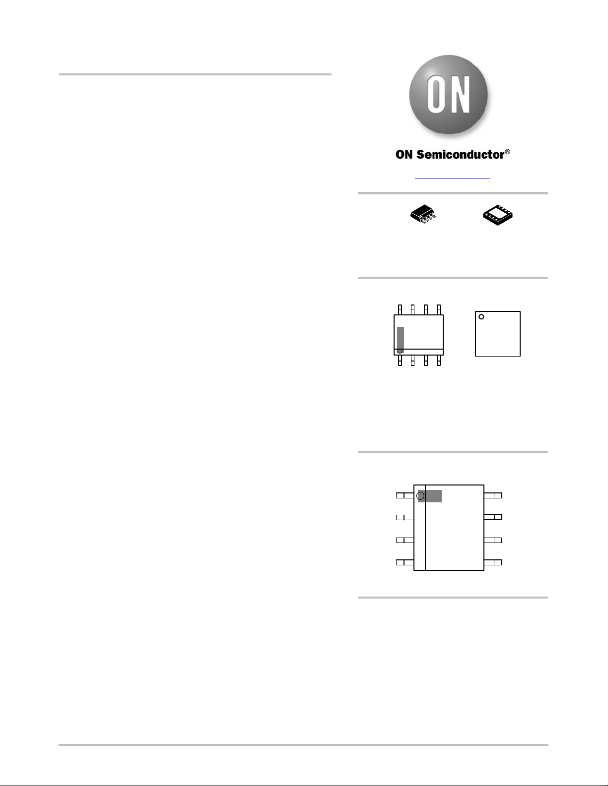
www.onsemi.com
8
1
SOIC−8
D SUFFIX
CASE 751AZ
MARKING DIAGRAMS
8
NV7428xx
ALYW G
G
1
A = Assembly Location
L = Wafer Lot
Y = Year
W = Work Week
G = Pb−Free Package
(Note: Microdot may be in either location)
PIN ASSIGNMENT
1
V
S
2
EN
3
GND
4
LIN
ORDERING INFORMATION
See detailed ordering, marking and shipping information in the
package dimensions section on page 17 of this data sheet.
NCV7428
(Top View)
1
DFN8
MW SUFFIX
CASE 506DG
1
NV7428xx
ALYWG
G
8
7
6
5
V
OUT
RSTN
TxD
RxD
© Semiconductor Components Industries, LLC, 2016
November, 2018 − Rev. 7
1 Publication Order Number:
NCV7428/D
Page 2
NCV7428
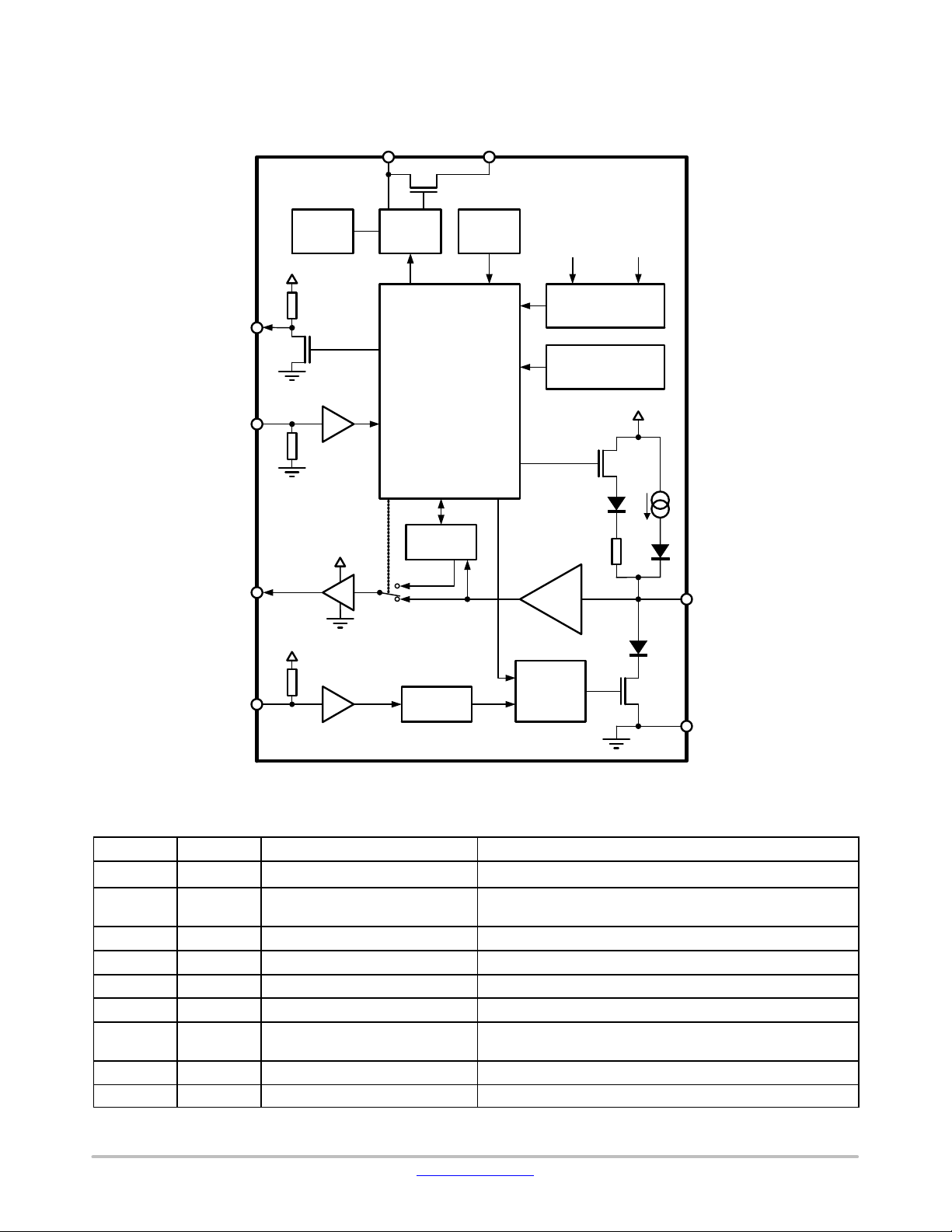
Block Diagram
RSTN
EN
RxD
V
OUT
V
S
NCV7428
V−regREF
V
OUT
Control Logic
V
OUT
Wakeup
Detection
LIN Wakeup
LIN Active
OSC
V
OUT
Undervoltage
Receiver
Detection
Thermal
Shutdown
V
S
V
S
LIN
V
OUT
Driver &
Slope
TxD
Timeout
Control
GND
Figure 1. Block Diagram
Table 1. PIN DESCRIPTION
Pin Number Pin Name Pin Type Pin Function
1 V
2 EN LV LIN enable input;
3 GND Ground connection Ground connection
4 LIN LIN bus interface LIN bus line
5 RxD LV digital output; push−pull Output of data received on LIN bus
6 TxD LV digital input; internal pull−up Input of the data to be transmitted from LIN bus
7 RSTN LV digital output;
8 V
EP EP Exposed Pad Connect to GND or leave floating
NOTE: (LV = Low Voltage; HV = High Voltage)
S
OUT
Battery supply input Principle power supply of the device
Input of the LIN block enable signal
internal pull−down
System reset
open drain; internal pull−up
LV supply output Output of the 5 V or 3.3 V/70 mA low−drop regulator (for the MCU)
www.onsemi.com
2
Page 3
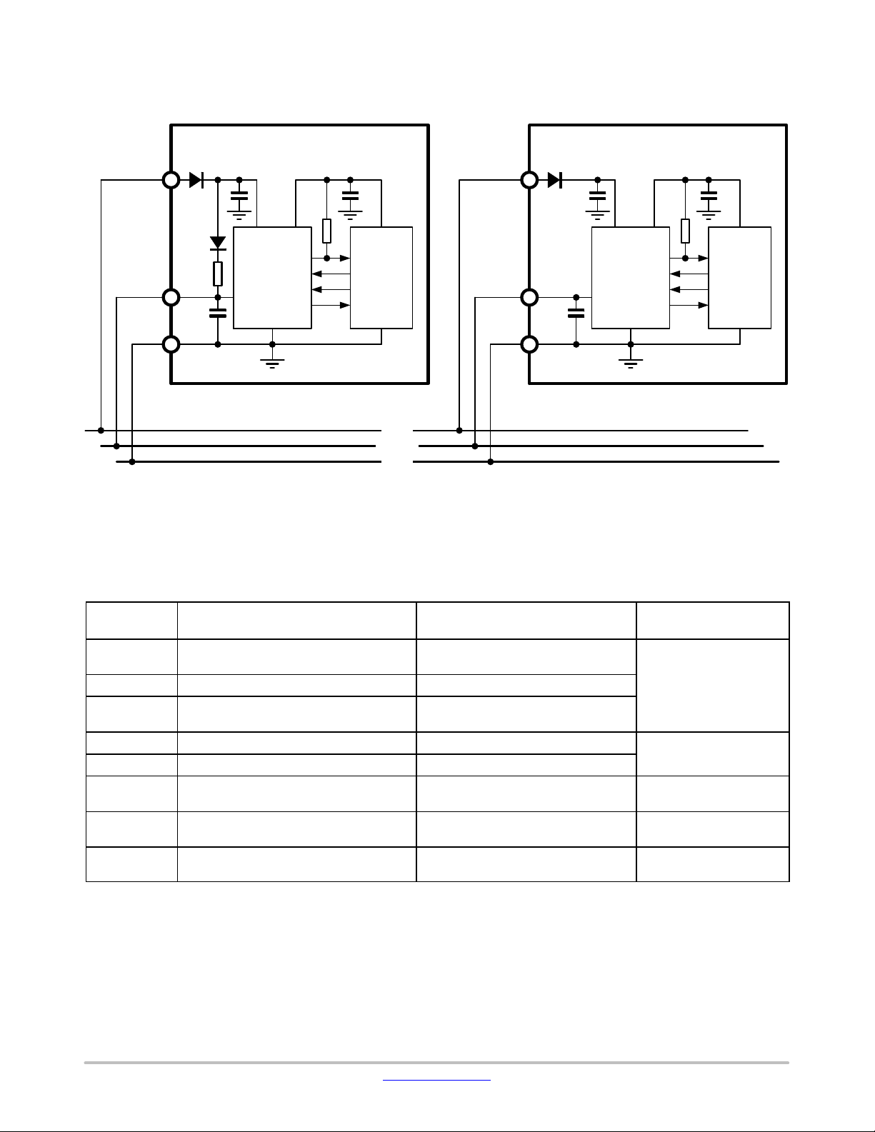
NCV7428
Application Information
VBAT
LIN
GND
D
R
C
D
REV
PU_LIN
PU_LIN
LIN_M
C
VS
LIN
V
S
GND
R
V
OUT
RSTN
EN
TxD
NCV7428
RxD
ECU1
PU_RSTN
C
VOUT
(MASTER)
V
CC
MCU
GND
KL30
LIN−BUS
KL31
VBAT
LIN
GND
D
REV
C
VS
PU_RSTN
R
V
V
S
OUT
RSTN
EN
LIN
C
LIN_S
TxD
NCV7428
RxD
GND
ECU2
C
VOUT
(SLAVE)
V
MCU
GND
Figure 2. Example Application Diagram
External Components
Overview of external components from application schematic in Figure 2 is given in Table 2 together with their recommended
or required values.
CC
Table 2. EXTERNAL COMPONENTS OVERVIEW
Component
Name
D
REV
C
C
VOUT
D
PU_LIN
R
PU_LIN
C
LIN_M
C
LIN_S
R
PU_RSTN
VS
Reverse polarity protection diode parameters application−specific;
Filtering capacitor for the battery input recommended >100 nF ceramic
Voltage regulator output filtering and
Master node Pull−up diode on LIN line
Master node Pull−up resistor on LIN line
Filtering capacitor on LIN line (Master node) typically 1 nF optional; is function of the
Filtering capacitor on LIN line (Slave node) typically 100 pF – 220 pF optional; is function of the
Pull−up resistor at RSTN pin
Description Value Note
stabilization capacitor
e.g. 0.5 A / 50 V
> 1.8 mF, ESR < 7 W
1 kW nominal, ≥500 mW
recommended 10 kW nominal
required values and types
depend on the V
and the application needs
OUT
load
required only for master
LIN node
entire LIN network
entire LIN network
optional; depends on
application needs
www.onsemi.com
3
Page 4
NCV7428
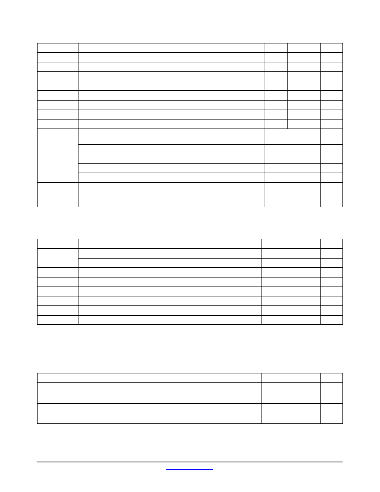
Table 3. ABSOLUTE MAXIMUM RATINGS
Symbol Parameter Min Max Units
V
S
V
OUT
V
LIN
V
Dig_IO_inputs
V
Dig_IO_outputs
T
AMB
T
J
T
STG
V
ESD
MSL Moisture Sensitivity Level SOIC
T
SLD
Stresses exceeding those listed in the Maximum Ratings table may damage the device. If any of these limits are exceeded, device functionality
should not be assumed, damage may occur and reliability may be affected.
1. For information, please refer to our Soldering and Mounting Techniques Reference Manual, SOLDERRM/D.
Maximum DC voltage at VS pin −0.3 45 V
Maximum voltage at V
pin −0.3 6 V
OUT
Maximum voltage at LIN bus pin −45 45 V
Maximum voltage at digital input pins (TxD, EN) −0.3 45 V
Maximum voltage at digital output pins (RxD, RSTN) −0.3 V
+0.3 V
OUT
Ambient temperature range −40 +125 °C
Junction temperature range −40 +170 °C
Storage temperature range −55 +150 °C
System ESD at pins VS, LIN as per IEC 61000−4−2: 330 W / 150 pF
≥ ±14
kV
(Verified by external test house)
Human body model at pins VS, LIN stressed towards GND with 1500 W / 100 pF ≥ ±8
Human body model at all pins as per JESD22−A114 / AEC−Q100−002
Charge device model at all pins as per JESD22−C101 / AEC−Q100−011
Machine model; (200 pF; 0.75 mH; 10 W) as per JESD22−A115 / AEC−Q100−003
≥ ±4
≥ ±500
±200 V
kV
kV
2
DFN
1
Lead temperature Soldering − Reflow (SMD styles only), Pb−Free (Note 1) 260 °C
V
−
Table 4. OPERATING RANGES
Symbol Parameter Min Max Units
V
S
VS operating voltage for parametric operation (Note 2) 5.5 28 V
VS operating voltage for limited operation (Note 2) 4 28 V
V
OUT5
V
OUT33
I
VOUT
V
LIN
V
Dig_IO_inputs
V
Dig_IO_outputs
Regulated voltage at V
Regulated voltage at V
Current delivered by the V
Operating voltage at LIN bus pin 0 V
supply output for 5 V versions 4.9 5.1 V
OUT
supply output for 3.3 V versions 3.234 3.366 V
OUT
regulator 70 mA
OUT
S
Operating voltage at digital input pins (TxD, EN) 0 5.5 V
Operating voltage at digital output pins (RxD, RSTN) 0 V
OUT
V
V
Functional operation above the stresses listed in the Recommended Operating Ranges is not implied. Extended exposure to stresses beyond
the Recommended Operating Ranges limits may affect device reliability.
2. Below 5.5 V at V
specifications as required by SAE J2602. It is ensured by the battery monitoring circuit. Above 28 V at V
operational (LIN pin toggling) but parameters cannot be guaranteed. For higher battery voltage operation above 28 V, LIN pull−up resistor
pin in normal mode, the bus will either stay recessive or comply with the voltage level specifications and transition time
S
pin, LIN communication is
S
must be selected large enough to avoid clamping of LIN pin by voltage drop over external pull−up resistor and LIN pin min current limitation.
Table 5. THERMAL CHARACTERISTICS
Rating Symbol Value Unit
Thermal Characteristics, SOIC−8 (Note 3)
Thermal Characteristics, DFN−8 (Note 3)
3. Refer to ELECTRICAL CHARACTERISTICS, RECOMMENDED OPERATING RANGES and/or APPLICATION INFORMATION for Safe
Operating parameters.
4. Values based on test board according to EIA/JEDEC Standard JESD51−3, signal layer with 10% trace coverage.
5. Values based on test board according to EIA/JEDEC Standard JESD51−7, signal layers with 10% trace coverage for the signal layer and
4 thermal vias connected between exposed pad and first inner Cu layer.
Thermal Resistance Junction−to−Air, Free air, 1S0P PCB (Note 4)
Thermal Resistance Junction−to−Air, Free air, 2S2P PCB (Note 5)
Thermal Resistance Junction−to−Air, Free air, 1S0P PCB (Note 4)
Thermal Resistance Junction−to−Air, Free air, 2S2P PCB (Note 5)
R
q
JA
R
q
JA
R
q
JA
R
q
JA
125
75
133
55
°C/W
°C/W
°C/W
°C/W
www.onsemi.com
4
Page 5
NCV7428
Definitions
The characteristics defined in this section are guaranteed within the operating ranges listed in Table 4, unless stated
otherwise. All voltages are referenced to GND (Pin 3). Positive currents flow into the respective pin.
Table 6. DC CHARACTERISTICS (V
specified. Typical values are given at V
Symbol
Parameter Conditions Min Typ Max Unit
= 5.5 V to 28 V; TJ = −40°C to +150°C; Bus Load = 500 W (VS to LIN); unless otherwise
S
= 12 V and TJ = 25°C, unless otherwise specified.)
S
SUPPLY MONITORING
V
S_PORH
V
S_PORL
V
OUT_RES_5
V
OUT_RES_33
V
OUT_RES_hys5
V
OUT_RES_hys33VOUT
VS threshold for the power−up
of the circuit
VS threshold for the Shutdown
of the circuit
V
monitoring threshold
OUT
NV7428−5
V
monitoring threshold
OUT
NV7428−3
V
monitoring threshold
OUT
hysteresis for NV7428−5
monitoring threshold
hysteresis for NV7428−3
VS rising 3.3 4 V
VS falling 2.2 3 V
V
falling 4.55 4.75 V
OUT
V
falling 2.97 3.135 V
OUT
0.1 V
0.06 V
CURRENT CONSUMPTION
I
VS_LIN_Active_recVS
I
VS_LIN_Wakeup
I
VS_Sleep
V
REGULATOR
OUT
V
OUT_5
V
OUT_33
V
OUT_5_EMC
supply current LIN Active, LIN bus recessive 1.8 mA
VS supply current (Note 8) Standby mode; LIN Wakeup,
LIN bus recessive; I
VS = 13.5 V, TJ < 105°C
VOUT
= 0 mA
VS supply current (Note 8) Sleep mode; LIN Wakeup, LIN bus
V
regulator output voltage
OUT
(Note 6)
V
regulator output voltage
OUT
(Note 6)
V
regulator output voltage
OUT
under EMC (Note 8)
recessive; V
VS = 13.5 V, TJ < 105°C
V
regulator active,
OUT
0 < I
VOUT
regulation, VS = 5.5 V to 28 V
V
regulator active,
OUT
0 < I
VOUT
regulation, V
DPI EMC test applied to LIN pin.
No bus capacitor. SOIC8 package;
off, V
OUT
OUT
< 70 mA, Static
< 70 mA, Static
= 4.5 V to 28 V
S
< 0.5 V
4.9 5 5.1 V
3.234 3.3 3.366 V
4.85 5 5.15 V
25 33
12 18
mA
mA
(Note 7)
V
OUT_33_EMC
V
regulator output voltage
OUT
under EMC (Note 8)
DPI EMC test applied to LIN pin.
No bus capacitor. SOIC8 package;
3.201 3.3 3.399 V
(Note 7)
I
LIM_VOUT
V
DROP_VOUT
I
SINK_VOUT
C
VOUT
V
current limitation V
OUT
Drop−out voltage between V
and V
OUT
V
sink current V
OUT
V
regulator filtering
OUT
capacitance (Note 9)
regulator active;
OUT
current flowing to V
5.5 V < VS < 40 V;
S
I
= 70 mA
VOUT
regulator active, current
OUT
flowing into the V
Equivalent series resistance < 7 W
OUT
OUT
pin
load
70 120 350 mA
0.55 V
100 240 400
1.8 10
mA
mF
Product parametric performance is indicated in the Electrical Characteristics for the listed test conditions, unless otherwise noted. Product
performance may not be indicated by the Electrical Characteristics if operated under different conditions.
6. In case LIN bus capacitor of at least 82 pF is not used V
7. Tested according to: LIN Conformance Test Specification Package for LIN 2.1, October 10
OUT_5_EMC
and V
OUT_33_EMC
needs to be taken into account.
th, 2008. Verified by external test house.
8. Values based on design and characterization. Not tested in production.
9. In parallel with this capacitor any other capacitor can be placed with no limit to ESR and capacitance value
10.The voltage drop in Normal mode between LIN and V
at the switch is negligible. See Figure 1.
pin is the sum of the diode drop and the drop at serial pull−up resistor. The drop
S
www.onsemi.com
5
Page 6
NCV7428
Table 6. DC CHARACTERISTICS (V
specified. Typical values are given at V
= 5.5 V to 28 V; TJ = −40°C to +150°C; Bus Load = 500 W (VS to LIN); unless otherwise
S
= 12 V and TJ = 25°C, unless otherwise specified.)
S
Symbol UnitMaxTypMinConditionsParameter
LIN TRANSMITTER
V
LIN_dom_LoSup
V
LIN_dom_HiSup
V
LIN_REC
I
LIN_lim
R
slave
C
LIN
LIN dominant output voltage TxD = Low; VS = 7.3 V 1.2 V
LIN dominant output voltage TxD = Low; VS = 18 V 2.0 V
LIN recessive output voltage
Short circuit current limitation V
TxD = High; I
= VS = 18 V 40 200 mA
LIN
= 10 mA (Note 10)
LIN
Internal Pull−up Resistance LIN Normal or Receive−only mode 20 33 47
VS – 1.5 V
S
kW
Capacitance at pin LIN (Note 8) 20 30 pF
V
LIN Receiver
V
bus_dom
V
bus_rec
V
rec_dom
V
rec_rec
V
rec_cnt
V
rec_hys
I
LIN_off_dom
I
LIN_off_dom_wake
I
LIN_off_rec
I
LIN_no_GND
I
LIN_no_VBB
Bus voltage for Dominant state 0.4 V
Bus voltage for Recessive state 0.6 V
Receiver threshold LIN bus going from Recessive to
0.4 0.6 V
Dominant
Receiver threshold LIN bus going from Dominant to
0.4 0.6 V
Recessive
Receiver center voltage (V
Receiver hysteresis V
LIN output current,
Bus in dominant state
LIN output current,
Bus in dominant state
LIN output current,
Bus in recessive state
LIN Active Mode, Driver Off;
V
LIN Wakeup Mode;
V
Driver Off; VS < 18 V;
V
LIN current with missing GND VS = GND = 12 V; 0 < V
LIN current with missing V
S
VS = GND = 0 V; 0 < V
rec_dom
rec_rec
= 12 V, V
S
= 12 V, V
S
< V
S
LIN
+ V
− V
< 18 V
)/2 0.475 0.525 V
rec_rec
rec_dom
0.05 0.175 V
−1 mA
= 0 V
LIN
−20 −15 −2
= 0 V
LIN
< 18 V −1 1 mA
LIN
< 18 V 5
LIN
1
S
S
S
S
S
S
mA
mA
mA
PIN EN
V
IL_EN
V
IH_EN
R
pulldown_EN
Low−level input voltage −0.3 0.8 V
High−level input voltage 2 5.5 V
Pull−down resistance to GND 55 100 185
kW
PIN TxD
V
IL_TxD
V
IH_TxD
R
pullup_TxD
I
leak_TxD
Low−level input voltage −0.3 0.8 V
High−level input voltage 2 5.5 V
Pull−up resistance to V
OUT
Leakage current V
TxD
= V
= 5.5 V −1 0 1
OUT
55 100 185
kW
mA
PIN RSTN
I
OL_RSTN
V
OL_RSTN
R
pullup_RSTN
Low−level output driving current VS = 4 V to 28 V; V
Low−level output voltage
Pull−up resistance to V
OUT
VS = 2 V to 4 V; V
5.5 V; I
VS < 2 V; V
I
RSTN
= 100 mA
RSTN
OUT
= 100 mA
= 1 V to 5.5 V;
= 0.4 V 4 30 mA
RSTN
= 0 V to
OUT
55 100 185
0.1 V
0.1 V
OUT
OUT
kW
Product parametric performance is indicated in the Electrical Characteristics for the listed test conditions, unless otherwise noted. Product
performance may not be indicated by the Electrical Characteristics if operated under different conditions.
6. In case LIN bus capacitor of at least 82 pF is not used V
7. Tested according to: LIN Conformance Test Specification Package for LIN 2.1, October 10
OUT_5_EMC
and V
OUT_33_EMC
needs to be taken into account.
th, 2008. Verified by external test house.
8. Values based on design and characterization. Not tested in production.
9. In parallel with this capacitor any other capacitor can be placed with no limit to ESR and capacitance value
10.The voltage drop in Normal mode between LIN and V
at the switch is negligible. See Figure 1.
pin is the sum of the diode drop and the drop at serial pull−up resistor. The drop
S
www.onsemi.com
6
Page 7

NCV7428
Table 6. DC CHARACTERISTICS (V
specified. Typical values are given at V
= 5.5 V to 28 V; TJ = −40°C to +150°C; Bus Load = 500 W (VS to LIN); unless otherwise
S
= 12 V and TJ = 25°C, unless otherwise specified.)
S
Symbol UnitMaxTypMinConditionsParameter
PIN RSTN
V
S_DigOut_Low
VS level guaranteeing Low level
at RSTN pin
Shutdown mode; Low level guaranteed for V
S
> V
S_DigOut_Low
2 V
PIN RxD
I
OL_RXD
I
OH_RXD
Low−level output driving current V
High−level output driving current V
= 0.4 V 0.4 mA
RxD
= V
RXD
− 0.4 V −0.16 mA
OUT
THERMAL SHUTDOWN
T
J_SD
T
J_SD_hys
Junction temperature for ther-
160 180 200 °C
mal Shutdown
Thermal Shutdown hysteresis 10 °C
Product parametric performance is indicated in the Electrical Characteristics for the listed test conditions, unless otherwise noted. Product
performance may not be indicated by the Electrical Characteristics if operated under different conditions.
6. In case LIN bus capacitor of at least 82 pF is not used V
7. Tested according to: LIN Conformance Test Specification Package for LIN 2.1, October 10
OUT_5_EMC
and V
OUT_33_EMC
needs to be taken into account.
th, 2008. Verified by external test house.
8. Values based on design and characterization. Not tested in production.
9. In parallel with this capacitor any other capacitor can be placed with no limit to ESR and capacitance value
10.The voltage drop in Normal mode between LIN and V
at the switch is negligible. See Figure 1.
pin is the sum of the diode drop and the drop at serial pull−up resistor. The drop
S
www.onsemi.com
7
Page 8

NCV7428
Table 7. AC CHARACTERISTICS (V
parameters, the following bus loads are considered: L1 = 1 kW / 1 nF; L2 = 660 W / 6.8 nF; L3 = 500 W / 10 nF)
Symbol
= 5.5 V to 28 V; TJ = −40°C to +150°C; unless otherwise specified. For the transmitter
S
Parameter Conditions Min Ty p Max Unit
LIN TRANSMITTER
D1 Duty Cycle 1 =
t
BUS_REC(min)
D2 Duty Cycle 2 =
t
BUS_REC(max)
D3 Duty Cycle 3 =
t
BUS_REC(min)
D4 Duty Cycle 4 =
t
BUS_REC(max)
t
fallNS
t
riseNS
t
symNS
t
fallLS
t
riseLS
t
tx_prop_down
t
tx_prop_up
t
TxD_timeout
LIN falling edge normal slope Normal Mode; VS = 12 V 22.5
LIN rising edge normal slope Normal Mode; VS = 12 V 22.5
LIN slope symmetry normal slope Normal Mode; VS = 12 V −4 0 4
LIN falling edge low slope (Note 12) Normal Mode; VS = 12 V 45
LIN rising edge low slope (Note 12) Normal Mode; VS = 12 V 45
Propagation Delay of TxD to LIN.
TxD high to low
Propagation Delay of TxD to LIN.
TxD low to high
TxD dominant timeout TxD = Low; LIN dominant
/ (2 x t
/ (2 x t
/ (2 x t
/ (2 x t
BIT
BIT
BIT
BIT
)
)
)
)
TH
REC(max)
TH
DOM(max)
t
BIT
VS = 7 V to 18 V
TH
REC(min)
TH
DOM(min)
t
BIT
V
= 7.6 V to 18 V
S
TH
REC(max)
TH
DOM(max)
t
BIT
V
= 7 V to 18 V
S
TH
REC(min)
TH
DOM(min)
t
BIT
VS = 7.6 V to 18 V
= 50 ms
= 50 ms
= 96 ms
= 96 ms
= 0.744 x V
= 0.581 x V
= 0.422 x V
= 0.284 x V
= 0.778 x V
= 0.616 x V
= 0.389 x V
= 0.251 x V
0.396 0.5
S
S
S
S
0.5 0.581
S
0.417 0.5
S
S
0.5 0.590
S
(Note 11) 10
(Note 11) 10
9 13 24 ms
timeout enabled
LIN RECEIVER
t
rec_prop_down
t
rec_prop_up
t
rec_sym
t
LIN_wake
Propagation delay of receiver falling
edge
Propagation delay of receiver rising
edge
Propagation delay symmetry t
rec_prop_down
t
rec_prop_up
−
Dominant duration for wakeup LIN in wakeup mode 30 80 150
0.1 6
0.1 6
−2 2
MODE TRANSITIONS AND TIMEOUTS
t
sample_txd
t
mode
t
lp_mode
t
reset
t
VOUT_RES_filt
Low power mode entry EN to TxD
sampling point delay
Normal mode or Reset mode transition time
Low power mode transition time
(Standby or Sleep)
RSTN pulse extension Figure 6, Figure 7, Figure
Undervoltage detection filter time Figure 6 13 25 55
Normal mode:
Figure 9, Figure 10
Low power mode:
Figure 9, Figure 10
Normal mode:
Figure 9, Figure 10
8
13 25 55
13 25 55
27 45 91
3 5 10 ms
11.Values based on design and characterization. Not tested in production.
12.For low slope versions only (NV7428L5 and NV7428L3)
ms
ms
ms
ms
ms
ms
ms
ms
ms
ms
ms
ms
ms
ms
ms
www.onsemi.com
8
Page 9

NCV7428
Functional Description
VS Supply Input
VS pin of NCV7428 is typically connected to the car
battery through a reverse−protection diode and can be
exposed to all relevant automotive disturbances (ISO7637
pulses, system ESD ...). V
supplies mainly the integrated
S
LIN transceiver. Filtering capacitors should be connected
between V
During power−up of the battery supply, V
V
S_PORH
– the internal state machine is initiated and the V
and GND.
S
pin must reach
S
level in order for the circuit to become functional
OUT
regulator is activated. The circuit remains functional until
V
falls back below V
S
level, when the device enters
S_PORL
the Shutdown mode.
VOUT Low−drop Voltage Regulator
The application low−voltage supply is provided by an
integrated low−drop voltage regulator delivering a 5 V or
3.3 V output V
. It is able to deliver up to 70 mA with
OUT
given precision and is primarily intended to supply the
application microcontroller unit (MCU) and related 5 V or
3.3 V loads (e.g. its own MCU−related digital inputs/
outputs). An external capacitor needs to be connected on
V
pin in order to ensure the regulator’s stability and to
OUT
filter the disturbances caused by the connected loads.
All low−voltage digital pins are related to V
LIN Transceiver
OUT
.
NCV7428 integrates on−chip LIN transceiver interface
between physical LIN bus and the LIN protocol controller.
This LIN physical layer is compatible to LIN2.x and
J2602 specifications.
NCV7428 LIN2.2 compliant physical layer can be
combined on the network with all previous LIN physical
layers.
NCV7428 LIN transceiver consists of a transmitter,
receiver and wakeup detector. The LIN transceiver can be
connected to the bus line via LIN pin, and to the digital
control through pins TxD and RxD. The functional mode of
the LIN transceiver depends on the operating mode and on
EN pin state – see Figure 3. The LIN transceiver is supplied
directly from the V
pin.
S
LIN Operating Modes
In LIN Active mode the transceiver can transmit and
receive data via LIN bus with speed up to 20 kBaud for
normal slope mode and 10 kBaud/s for low slope version.
The transmit data stream of the LIN protocol is present on
the TxD pin and converted by the transmitter into a LIN bus
signal with controlled slew rate to minimize EMC emission.
The receiver consists of the comparator that has a threshold
with hysteresis in respect to the supply voltage and an input
filter to remove bus noise. The LIN output is pulled HIGH
via an internal pull−up resistor (typ. 30 kW). For master
applications, it is needed to put an external resistor (typ.
1kW) with a serial diode between LIN and V
. The mode
S
selection is done by EN = High.
The transmission is only initiated with the TxD falling
edge in LIN Active mode. Entering this mode with TxD
already Low will not lead to transmitting bus Dominant
signal.
When leaving Normal mode (EN pin falling edge), the
transmitter is deactivated immediately.
The LIN Wakeup mode can be entered if the EN pin is
Low. The LIN receiver stays active to be able to detect a
remote wake−up via bus. The LIN transmitter is disabled
and the slave internal termination resistor of 30 kW between
LIN and V
is disconnected in order to minimize current
S
consumption. Only a pull−up current source between Vs and
LIN is active. The valid LIN wakeup event causes driving
RxD Low until EN pin is pulled High.
A Wakeup pattern that is initiated in LIN Active mode and
ends in LIN Wakeup mode is also considered a valid Wakeup
event.
The LIN Wakeup mode is also forced if the device enters
to the Sleep operating mode.
The LIN Off mode provides extreme low current
consumption, LIN transceiver is fully deactivated. Pin RxD
stays High (as long as V
is provided) and logical level
OUT
on TxD is ignored.
The bus pin is internally pulled to V
(thus limiting V
consumption in case of a permanent LIN
S
with a current source
S
short to GND).
This mode is entered when NCV7428 is in Shutdown
mode (V
T
J_SD
S
< V
) or in Thermal Shutdown mode (TJ >
S_PORL
).
www.onsemi.com
9
Page 10

NCV7428
LIN Off LIN Wakeup LIN ActiveLIN Mode
Bus Pin
Pull−up
recessive
LIN
dominant
TxD
RxD
EN
recessive
< t
LIN_wake
ignored
ignored
Current Source 30 kWResistor
t
TxD_timeout
LIN Wakeup
detected
LIN Active
mode set
Figure 3. LIN Modes
t
LIN_wake
LIN
dominant
RxD
EN
LIN Wakeup
detected
Figure 4. LIN Wakeup Detection
LIN Active
mode restored
www.onsemi.com
10
Page 11

NCV7428
Operating Modes
The principal operating modes of NCV7428 are shown in Figure 5 and described in the following paragraphs.
VS power−up
Any mode
V
S<VS_PORL
SHUTDOWN
−V
:off
OUT
−RSTN: Low
−LIN: Off mode
−RxD: pulled to V
OUT
VS>VS_
and TJ< T
PORH
J_SD
RESET
−V
:on
OUT
−RSTN: Low
−LIN: Wakeup mode
−RxD: Low after Wakeup/
High otherwise
Any mode
(except for shutdown)
TJ> T
J_S D
THERMAL
SHUTDOWN
:off
−V
OUT
−RSTN: Low
−LIN: Wakeup mode
−RxD: Low after Wakeup/
pulled to V
TJ< T
J_S D
otherwise
OUT
STANDBY
−V
:on
OUT
−RSTN: High
−LIN: Wakeup mode
−RxD: Low after Wakeup/
High otherwise
EN = 1
−V
:on
OUT
EN = 0
and
TxD = 1
−RSTN: High
−LIN: Active mode
−RxD: Received LIN Data
−V
:off
OUT
−RSTN: Low
−LIN: Wakeup mode
−RxD: pulled to V
Figure 5. Operating Modes
NORMAL
LIN_EN = 0
and
TxD = 0
SLEEP
OUT
LIN wakeup
or
EN = 1
www.onsemi.com
11
Page 12

NCV7428
Shutdown Mode
The Shutdown mode is a passive state, in which all
NCV7428 resources are inactive. The Shutdown mode
provides a defined starting point for the circuit in case of
supply undervoltage, thermal Shutdown or the first supply
connection.
On−chip power−supply V
is switched off and the LIN
OUT
pin remains passive so that it does not disturb the
communication of other nodes connected to the LIN bus.
RxD pin stays pulled to V
. No wakeups can be detected.
OUT
RSTN pin is forced Low – RSTN Low level is guaranteed
for V
supply above V
S
S_DigOut_Low
.
The Shutdown mode is entered asynchronously whenever
the V
level falls below the power−on−reset level V
S
The Shutdown mode is left only when the V
exceeds the high power−on−reset level V
junction temperature is below T
. When exiting the
J_SD
S_PORH
S_PORL
supply
S
while
Shutdown mode, NCV7428 always enters the Reset mode.
RESET Mode
The Reset mode is a transient mode providing a defined
RSTN pulse for the application microcontroller.
V
supply is kept active. The LIN pin is passive so that
OUT
it does not disturb the communication of other nodes
connected to the bus. RxD pin is High if no wakeup was
detected, RxD Low level indicates pending LIN wakeup.
Pin RSTN is forced Low.
Reset mode will be entered as a consequence of one of the
following events:
• Shutdown mode is exited
• Thermal Shutdown mode is exited
• V
voltage falls below V
OUT
OUT_RES
level
• LIN wakeup or EN = High was detected in Sleep mode
Normally, the Reset mode is left when V
above V
OUT_RES
threshold and defined time t
The RSTN pin is internally released to High and the chip
then goes to the Normal or Standby mode, depending on EN
state.
voltage is
OUT
reset
elapses.
High when leaving Reset mode – t
reset
(Figure 8).
LIN transceiver is in Active mode. V
OUT
RSTN remains High.
Standby Mode
Standby mode is entered from Normal mode after host
request – EN pin falling edge followed by TxD pin High.
TxD is sampled t
sample_txd
after EN edge (Figure 9). Standby
mode is also entered if EN pin is Low when leaving Reset
mode – t
time elapsed (Figure 7).
reset
LIN transceiver is in Wakeup mode – RxD pin is latched
Low after valid Wakeup recognition until Normal mode is
.
requested. V
Sleep Mode
is kept active. Pin RSTN remains High.
OUT
Sleep mode can be only entered from Normal mode after
a host request – EN pin falling edge followed by TxD pin
Low. LIN transmitter is blocked immediately after EN pin
falling edge, therefor TxD pin and EN pin can be set Low at
the same moment. TxD is sampled t
sample_txd
edge (Figure 10).
regulator is switched off, LIN transceiver is in the
V
OUT
Wakeup mode.
If LIN wakeup is detected or EN goes High, Reset mode
is entered. LIN wakeup is signaled by RxD, which remains
Low until Normal mode is restored (EN is High).
Thermal Shutdown
The device junction temperature is monitored in order to
avoid permanent degradation or damage of the chip.
Junction temperature exceeding the Shutdown level T
puts the chip into Thermal Shutdown mode.
In Thermal Shutdown mode, V
regulator is switched
OUT
off. LIN transceiver is in Wakeup mode and can detect bus
Wakeup. RxD pin stays pulled to V
or is driven Low
OUT
after valid Wakeup recognition. RSTN pin is pulled low. The
mode is automatically left only when the junction cools
down below the T
J_SD
threshold.
time elapsed
is kept on. Pin
after EN pin
J_SD
Normal Mode
Normal mode is entered from Standby mode after a host
request – driving EN pin High (Figure 9), or if EN pin is
www.onsemi.com
12
Page 13

NCV7428
V
V
OUT
V
OUT_RES
V
S_PORH
RSTN
EN
Operating
mode
V
S
t
VOUT_RES_filt
t
reset
Reset
EN
S
V
OUT
Figure 6. V
ignored
t
VOUT_RES_filt
Regulator Voltage Monitoring
OUT
t
VOUT_ RES_ filt
t
reset
<t
VOUT_RES_filt
StandbyResetShutdown Standby
TxD
RxD
RSTN
Operating
mode
V
OUT>VOUT_RES
Figure 7. Operating Modes, Transition from Reset to Standby Mode
LIN wakeup indication
t
reset
Reset
RSTN pulse released
ignored
Standby
EN sampled
www.onsemi.com
13
Page 14

NCV7428
EN
TxD
RxD
RSTN
Operating
mode
EN
V
OUT>VOUT_RES
ignored
ignored
LIN wakeup indication
t
reset
t
mode
Reset Normal
RSTN pulse released
EN sampled
Mode change
LIN wakeup flag cleared
Figure 8. Operating Modes, Transition from Reset to Normal Mode
TxD
LIN
RxD
RSTN
Operating
mode
TxD sampling point
ignored ignored
LIN transmission
blocked
LIN wakeup indication
t
sample_txd
Normal
t
lp_mode
Standby
Figure 9. Operating Modes, Transition from Normal to Standby Mode
t
mode
Normal
www.onsemi.com
14
Page 15

EN
NCV7428
TxD sampling point
TxD
LIN
RxD
RSTN
Operating
mode
ignored
LIN transmission
blocked
ignored
Normal
t
sample_txd
t
lp_mode
Figure 10. Operating Modes, Transition from Normal to Sleep Mode
TxD
t
BIT
t
BIT
50%
V
OUT
Sleep
OFF
t
mode
LIN wakeup
indication
Reset
TH
TH
TH
TH
LIN
REC(max)
DOM(max)
REC(min)
DOM(min)
t
BUS_dom(max)
t
BUS_dom(min)
t
BUS_rec(min)
t
BUS_rec(max)
Figure 11. Definition of LIN Duty Cycle Parameters
t
Thresholds of
receiving node 1
Thresholds of
receiving node 2
t
www.onsemi.com
15
Page 16

LIN
100%
NCV7428
0%
TxD
LIN
V
60%
40%
t
fall
60%
40%
t
rise
t
Figure 12. Definition of LIN Edge Parameters
t
BIT
t
BIT
50%
t
S
60% V
S
40% V
S
LIN
V
RxD
t
tx_prop_down
S
t
tx_prop_up
Figure 13. Definition of LIN Transmitter Timing Parameters
t
rec_prop_down
t
rec_prop_up
50%
Figure 14. Definition of LIN Receiver Timing Parameters
60% V
40% V
t
S
S
t
t
www.onsemi.com
16
Page 17

NCV7428
ORDERING INFORMATION
Part Number Description Marking Package Shipping
NCV7428D15R2G LIN transceiver with 5 V regulator NV7428−5
NCV7428D13R2G LIN transceiver with 3.3 V regulator NV7428−3
NCV7428D1L5R2G LIN transceiver with 5 V regulator,
low slope LIN
NCV7428D1L3R2G LIN transceiver with 3.3 V regulator,
low slope LIN
NCV7428MW5R2G LIN transceiver with 5 V regulator NV7428−5
NCV7428MW3R2G LIN transceiver with 3.3 V regulator NV7428−3
NCV7428MWL5R2G LIN transceiver with 5 V regulator,
low slope LIN
NCV7428MWL3R2G LIN transceiver with 3.3 V regulator,
low slope LIN
†For information on tape and reel specifications, including part orientation and tape sizes, please refer to our Tape and Reel Packaging
Specifications Brochure, BRD8011/D.
NV7428L5
NV7428L3
NV7428L5
NV7428L3
SOIC−8
(Pb−Free)
DFN8
Wettable Flanks
(Pb−Free)
3000 / Tape & Reel
3000 / Tape & Reel
†
www.onsemi.com
17
Page 18

MECHANICAL CASE OUTLINE
PACKAGE DIMENSIONS
1
SCALE 2:1
A
B
E
A3
A
PIN ONE
REFERENCE
2X
0.10 C
2X
0.05 C
0.10 C
D
TOP VIEW
DFN8, 3x3, 0.65P
CASE 506DG
ISSUE A
L
DETAIL A
ALTERNATE TERMINAL
CONSTRUCTION
DATE 28 APR 2016
NOTES:
1. DIMENSIONING AND TOLERANCING PER
ASME Y14.5M, 1994.
2. CONTROLLING DIMENSION: MILLIMETERS.
3. DIMENSION b APPLIES TO PLATED TERMINAL
AND IS MEASURED BETWEEN 0.15 AND
0.30mm FROM THE TERMINAL TIP.
4. COPLANARITY APPLIES TO THE EXPOSED
PAD AS WELL AS THE TERMINALS.
MILLIMETERS
DIM MIN MAX
A 0.80 1.00
A1 0.00 0.05
A3 0.20 REF
b 0.25 0.35
D 3.00 BSC
D2 2.30 2.50
E 3.00 BSC
E2 1.50 1.70
e 0.65 BSC
K
0.30 TYP
L 0.35 0.45
NOTE 4
0.05 C
DETAIL A
8X
L
K
SIDE VIEW
A1
D2
14
E2
58
8X
e/2
b
e
BOTTOM VIEW
RECOMMENDED
SOLDERING FOOTPRINT*
2.56
1.70
SEATING
C
PLANE
0.10 B
NOTE 3
0.05ACC
8X
0.60
3.30
GENERIC
MARKING DIAGRAM*
1
XXXXXX
XXXXXX
ALYWG
G
XXXXXX= Specific Device Code
A = Assembly Location
L = Wafer Lot
Y = Year
W = Work Week
G = Pb−Free Package
(Note: Microdot may be in either location)
*This information is generic. Please refer
to device data sheet for actual part
marking.
Pb−Free indicator, “G” or microdot “ G”,
may or may not be present.
0.65
PITCH
1
DIMENSIONS: MILLIMETERS
8X
0.40
*For additional information on our Pb−Free strategy and soldering
details, please download the ON Semiconductor Soldering and
Mounting Techniques Reference Manual, SOLDERRM/D.
DOCUMENT NUMBER:
DESCRIPTION:
ON Semiconductor and are trademarks of Semiconductor Components Industries, LLC dba ON Semiconductor or its subsidiaries in the United States and/or other countries.
ON Semiconductor reserves the right to make changes without further notice to any products herein. ON Semiconductor makes no warranty, representation or guarantee regarding
the suitability of its products for any particular purpose, nor does ON Semiconductor assume any liability arising out of the application or use of any product or circuit, and specifically
disclaims any and all liability, including without limitation special, consequential or incidental damages. ON Semiconductor does not convey any license under its patent rights nor the
rights of others.
© Semiconductor Components Industries, LLC, 2019
98AON10527G
DFN8 3X3, 0.65P
Electronic versions are uncontrolled except when accessed directly from the Document Repository.
Printed versions are uncontrolled except when stamped “CONTROLLED COPY” in red.
PAGE 1 OF 1
www.onsemi.com
Page 19

MECHANICAL CASE OUTLINE
PACKAGE DIMENSIONS
8
CASE 751AZ
1
SCALE 1:1
NOTES 4&5
D
D
NOTE 6
85
E E1
A
0.10 C D
2X
0.10 C
NOTES 4&5
D
L2
0.20 C
14
D
B
NOTE 6
TOP VIEW
b8X
0.25 A-B
NOTES 3&7
M
D
C
A2
0.10 C
A
A1
NOTE 8
SIDE VIEW
SIDE VIEW
e
C
SEATING
PLANE
END VIEW
RECOMMENDED
SOLDERING FOOTPRINT*
8X
0.76
8X
1.52
7.00
1
1.27
PITCH
*For additional information on our Pb−Free strategy and soldering
details, please download the ON Semiconductor Soldering and
Mounting Techniques Reference Manual, SOLDERRM/D.
DIMENSIONS: MILLIMETERS
SOIC−8
ISSUE B
45 CHAMFER5
h
L
DETAIL A
DETAIL A
NOTES:
1. DIMENSIONING AND TOLERANCING PER ASME Y14.5M, 1994.
2. CONTROLLING DIMENSION: MILLIMETERS.
3. DIMENSION b DOES NOT INCLUDE DAMBAR PROTRUSION.
H
C
NOTE 7
SEATING
PLANE
c
ALLOWABLE PROTRUSION SHALL BE 0.004 mm IN EXCESS OF
MAXIMUM MATERIAL CONDITION.
4. DIMENSION D DOES NOT INCLUDE MOLD FLASH, PROTRUSIONS
OR GATE BURRS. MOLD FLASH, PROTRUSIONS OR GATE BURRS
SHALL NOT EXCEED 0.006 mm PER SIDE. DIMENSION E1 DOES
NOT INCLUDE INTERLEAD FLASH OR PROTRUSION. INTERLEAD
FLASH OR PROTRUSION SHALL NOT EXCEED 0.010 mm PER SIDE.
5. THE PACKAGE TOP MAY BE SMALLER THAN THE PACKAGE BOT
TOM. DIMENSIONS D AND E1 ARE DETERMINED AT THE OUTER
MOST EXTREMES OF THE PLASTIC BODY AT DATUM H.
6. DIMENSIONS A AND B ARE TO BE DETERMINED AT DATUM H.
7. DIMENSIONS b AND c APPLY TO THE FLAT SECTION OF THE LEAD
BETWEEN 0.10 TO 0.25 FROM THE LEAD TIP.
8. A1 IS DEFINED AS THE VERTICAL DISTANCE FROM THE SEATING
PLANE TO THE LOWEST POINT ON THE PACKAGE BODY.
MILLIMETERS
DIM MIN MAX
A --- 1.75
A1 0.10 0.25
A2 1.25 ---
b 0.31 0.51
c 0.10 0.25
D 4.90 BSC
E 6.00 BSC
E1 3.90 BSC
e 1.27 BSC
h 0.25 0.41
L 0.40 1.27
0.25 BSC
L2
GENERIC
MARKING DIAGRAM*
8
XXXXX
ALYWX
G
1
XXXXX = Specific Device Code
A = Assembly Location
L = Wafer Lot
Y = Year
W = Work Week
G = Pb−Free Package
*This information is generic. Please refer
to device data sheet for actual part
marking. Pb−Free indicator, “G”, may
or not be present.
DATE 18 MAY 2015
DOCUMENT NUMBER:
DESCRIPTION:
ON Semiconductor and are trademarks of Semiconductor Components Industries, LLC dba ON Semiconductor or its subsidiaries in the United States and/or other countries.
ON Semiconductor reserves the right to make changes without further notice to any products herein. ON Semiconductor makes no warranty, representation or guarantee regarding
the suitability of its products for any particular purpose, nor does ON Semiconductor assume any liability arising out of the application or use of any product or circuit, and specifically
disclaims any and all liability, including without limitation special, consequential or incidental damages. ON Semiconductor does not convey any license under its patent rights nor the
rights of others.
© Semiconductor Components Industries, LLC, 2019
98AON34918E
SOIC−8
Electronic versions are uncontrolled except when accessed directly from the Document Repository.
Printed versions are uncontrolled except when stamped “CONTROLLED COPY” in red.
PAGE 1 OF 1
www.onsemi.com
Page 20

ON Semiconductor and are trademarks of Semiconductor Components Industries, LLC dba ON Semiconductor or its subsidiaries in the United States and/or other countries.
ON Semiconductor owns the rights to a number of patents, trademarks, copyrights, trade secrets, and other intellectual property. A listing of ON Semiconductor’s product/patent
coverage may be accessed at www.onsemi.com/site/pdf/Patent−Marking.pdf
ON Semiconductor makes no warranty, representation or guarantee regarding the suitability of its products for any particular purpose, nor does ON Semiconductor assume any liability
arising out of the application or use of any product or circuit, and specifically disclaims any and all liability, including without limitation special, consequential or incidental damages.
Buyer is responsible for its products and applications using ON Semiconductor products, including compliance with all laws, regulations and safety requirements or standards,
regardless of any support or applications information provided by ON Semiconductor. “Typical” parameters which may be provided in ON Semiconductor data sheets and/or
specifications can and do vary in different applications and actual performance may vary over time. All operating parameters, including “Typicals” must be validated for each customer
application by customer’s technical experts. ON Semiconductor does not convey any license under its patent rights nor the rights of others. ON Semiconductor products are not
designed, intended, or authorized for use as a critical component in life support systems or any FDA Class 3 medical devices or medical devices with a same or similar classification
in a foreign jurisdiction or any devices intended for implantation in the human body. Should Buyer purchase or use ON Semiconductor products for any such unintended or unauthorized
application, Buyer shall indemnify and hold ON Semiconductor and its officers, employees, subsidiaries, affiliates, and distributors harmless against all claims, costs, damages, and
expenses, and reasonable attorney fees arising out of, directly or indirectly, any claim of personal injury or death associated with such unintended or unauthorized use, even if such
claim alleges that ON Semiconductor was negligent regarding the design or manufacture of the part. ON Semiconductor is an Equal Opportunity/Affirmative Action Employer. This
literature is subject to all applicable copyright laws and is not for resale in any manner.
. ON Semiconductor reserves the right to make changes without further notice to any products herein.
PUBLICATION ORDERING INFORMATION
LITERATURE FULFILLMENT:
Email Requests to: orderlit@onsemi.com
ON Semiconductor Website: www.onsemi.com
TECHNICAL SUPPORT
North American Technical Support:
Voice Mail: 1 800−282−9855 Toll Free USA/Canada
Phone: 011 421 33 790 2910
Europe, Middle East and Africa Technical Support:
Phone: 00421 33 790 2910
For additional information, please contact your local Sales Representative
◊
www.onsemi.com
1
 Loading...