

Page 1
NCS36000
Passive Infrared (PIR)
Detector Controller
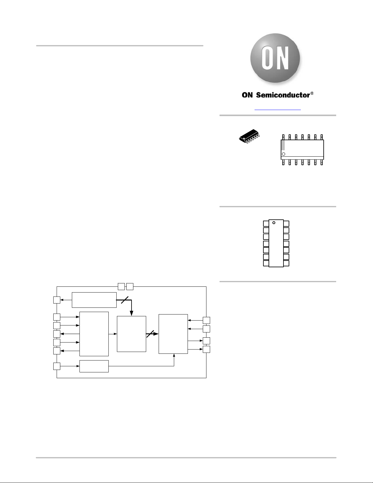
The NCS36000 is a fully integrated mixed−signal CMOS device
designed for low−cost passive infrared controlling applications. The
device integrates two low−noise amplifiers and a LDO regulator to
drive the sensor. The output of the amplifiers goes to a window
comparator that uses internal voltage references from the regulator.
The digital control circuit processes the output from the window
comparator and provides the output to the OUT and LED pin.
Features
• 3.0 − 5.75 V Operation
• −40 to 85°C
• 14 Pin SOIC Package
• Integrated 2−Stage Amplifier
• Internal LDO to Drive Sensor
• Internal Oscillator with External RC
• Single or Dual Pulse Detection
• Direct Drive of LED and OUT
• This is a Pb−Free Device
Typical Applications
• Automatic Lighting (Residential and Commercial)
• Automation of Doors
• Motion Triggered Events (Animal photography)
14VDD
7VSS
6VREF
LDO &
Voltage References
2
www.onsemi.com
MARKING
DIAGRAM
14
1
SOIC−14
D SUFFIX
CASE 751A
A = Assembly Location
WL = Wafer Lot
Y = Year
WW = Work Week
G = Pb−Free Package
14
NCS36000G
AWLYWW
1
PIN CONNECTIONS
OP2_O
OP2_N
OP1_O
OP1_N
OP1_P
VREF
VSS
1
2
3
4
5
6
7
(Top View)
14
13
12
11
10
9
8
VDD
OSC
MODE
NC
xLED_EN
LED
OUT
ORDERING INFORMATION
See detailed ordering and shipping information in the package
dimensions section on page 7 of this data sheet.
5OP1_P
4OP1_N
3OP1_O
2OP2_N
1OP2_O
13OSC
Amplifier
Circuit
System
Oscillator
Comparator
Figure 1. Simplified Block Diagram
© Semiconductor Components Industries, LLC, 2015
December, 2015 − Rev. 3
Window
12 MODE
Digital
2
Control
Circuit
1 Publication Order Number:
10 xLED_EN
9 LED
8 OUT
NCS36000/D
Page 2
NCS36000
PIN FUNCTION DESCRIPTION
Pin No. Pin Name Description
1 OP2_O Output of second amplifier
2 OP2_N Inverting input of second amplifier
3 OP1_O Output of first amplifier
4 OP1_N Inverting input of first amplifier
5 OP1_P Non−inverting input of first amplifier
6 VREF Regulated voltage reference to drive sensor
7 VSS Analog ground reference.
8 OUT CMOS output (10 mA Max)
9 LED CMOS output to drive LED (10mA Max)
10 xLED_EN Active low LED enable input
11 NC No Connect
12 MODE Pin used to select pulse count mode
13 OSC External oscillator to control clock frequency
14 VDD Analog power supply
ABSOLUTE MAXIMUM RATINGS
Rating Symbol Value Unit
Input Voltage Range (Note 1) V
Output Voltage Range V
Maximum Junction Temperature T
J(max)
Storage Temperature Range T
ESD Capability, Human Body Model (Note 2) ESD
ESD Capability, Machine Model (Note 2) ESD
Lead Temperature Soldering
T
Reflow (SMD Styles Only), Pb−Free Versions (Note 3)
in
out
STG
HBM
MM
SLD
−0.3 to 6.0 V
−0.3 to 6.0 V or (Vin + 0.3),
whichever is lower
140 °C
−65 to 150 °C
2 kV
200 V
260 °C
V
Stresses exceeding those listed in the Maximum Ratings table may damage the device. If any of these limits are exceeded, device functionality
should not be assumed, damage may occur and reliability may be affected.
1. Refer to ELECTRICAL CHARACTERISTICS and APPLICATION INFORMATION for Safe Operating Area.
2. This device series incorporates ESD protection and is tested by the following methods:
ESD Human Body Model tested per AEC−Q100−002 (EIA/JESD22−A114)
ESD Machine Model tested per AEC−Q100−003 (EIA/JESD22−A115)
Latchup Current Maximum Rating: v150 mA per JEDEC standard: JESD78
3. For information, please refer to our Soldering and Mounting Techniques Reference Manual, SOLDERRM/D
THERMAL CHARACTERISTICS
Rating Symbol Value Unit
Thermal Characteristics, DFN6, 3x3.3 mm (Note 4)
Thermal Resistance, Junction−to−Air (Note 5)
Thermal Reference, Junction−to−Lead2 (Note 5)
R
q
JA
R
Y
JL
Thermal Characteristics, TSOP−5 (Note 4)
Thermal Resistance, Junction−to−Air (Note 5)
4. Refer to ELECTRICAL CHARACTERISTICS and APPLICATION INFORMATION for Safe Operating Area.
5. Values based on copper area of 645 mm
2
(or 1 in2) of 1 oz copper thickness and FR4 PCB substrate.
R
q
JA
Will be Completed once
package and power
consumption is finalized
See note above.
°C/W
°C/W
www.onsemi.com
2
Page 3
NCS36000
OPERATING RANGES (Note 6)
Rating
Analog Power Supply V
Analog Ground Reference V
Supply Current (Standby, No Loads) I
Digital Inputs (MODE)
Digital Output (OUT, LED) Push−Pull Output (10 mA Load)
OP1_P (Sensor Input) (Note 7) AMP 1 IN 0.1 VDD −
Ambient Temperature T
6. Refer to ELECTRICAL CHARACTERISTICS and APPLICATION INFORMATION for Safe Operating Area.
7. Guaranteed By Design (Non−tested parameter).
Symbol Min Typ Max Unit
DD
SS
DD
V
ih
V
il
V
oh
V
ol
A
3.0 5.0 5.75 V
0.0 0.1 V
0.7 *
V
DD
V
DD
VDD +
VSS VDD *
0.67 *
V
DD
VSS VDD *
−40 85 °C
170m
0.3
0.28
V
DD
0.3
1.1
A
V
V
V
ELECTRICAL CHARACTERISTICS V
Parameter
= 1 V, Cin = 100 nF, C
in
Test Conditions Symbol Min Typ Max Unit
= 100 nF, for typical values TA = 25°C; unless otherwise noted.
out
LDO Voltage Reference
Output Voltage
VDD = 3.0 V to 5.75 V VREF 2.6 2.7 2.8 V
Supply Current VDD = 3.0 V to 5.75V IREF 20 50
Comparator High Trip Level V
Comparator Low Trip Level V
Reference voltage for non−inverting input of
second amplifier
h
l
V
m
2.413 2.5 2.588 V
1.641 1.7 1.760 V
2.007 2.1 2.174 V
System Oscillator
Oscillator Frequency
VDD = 5.0 V
= 220 kW
R
3
C2 = 100 nF
OSC 62.5 Hz
Window Comparator
Lower Trip Threshold
See Vl above
Higher Trip Threshold See Vh above
Differential Amplifiers (Amplifier Circuit)
DC Gain
VDD = 5.0 V (Note 8) Av 80 dB
Common−mode Input Range VDD = 5.0 V (Note 8) CMIR 0.1 VDD −
1.1
Power Supply Rejection Ratio VDD = 5.0 V (Note 8) PSRR 60 dB
Output Drive Current VDD = 5.0 V (Note 8) I
out1
25
POR
POR Release Voltage
V
POR
1.35 2.85 V
8. Guaranteed By Design (Non−tested parameter).
mA
V
mA
www.onsemi.com
3
Page 4

NCS36000
APPLICATIONS INFORMATION
Oscillator
The oscillator uses an external resistor and capacitor to set
the system clock frequency. Multiple clock frequencies can
be selected using different combinations of resistors and
capacitors. Figure 2 shows a simplifier block diagram for
the system oscillator.
VDD
14
OSC
13
Figure 2. Block Diagram of System Oscillator Circuit
LDO Regulator
−
+
−
+
SET
Q
S
CLR
Q
R
The LDO regulator provides the reference voltage for the
sensor and all other analog blocks within the system. The
nominal voltage reference for the sensor is 2.7 V ±5%. An
external capacitor is needed on the VREF pin to guarantee
stability of the regulator.
Differential Amplifiers
The two differential amplifiers can be configured as a
bandpass filter to condition the PIR sensor signal for the post
digital signal processing. The cutoff frequencies and
passband gain are set by the external components. See
Figure 5.
80
70
60
50
40
30
20
−1
10
0
10
1
10
Figure 3. Plot Showing Typical Magnitude Response
of Differential Amplifiers When Configured as a
Bandpass Filter
Window Comparator
The window comparator compares the voltage from the
second dif ferential amplifier to two reference voltages from
the LDO regulator. COMP_P triggers if OP2_O is greater
than the Vh voltage and COMP_N triggers if OP2_O is
lower than the Vl voltage. See Figures 4 and 5.
OP2_O
Vh
Vm
Vl
Vdd
Comp_P
Vss
Vdd
Comp_N
Vss
Figure 4. Plot Showing Functionality of Window Comparator for an Analog Input OP2_O
www.onsemi.com
4
Page 5

VREF
D
G
Sensor dependent
components
Figure 5. Figure Showing Simplified Block Diagram of Analog Conditioning Stages
NCS36000
VREF 6
1
Vh
OP2_O
Vl
LDO6
5
+
4
−
Application dependent
components
Vm
+
23
−
−
Comp_P
+
−
Comp_N
+
Vh
Vm
Vl
Digital Signal Processing Block (all times assume a
62.5 Hz system oscillator frequency)
The digital signaling processing block performs three
major functions.
The first function is that the device toggles LED during the
start−up sequencing at approximately two hertz regardless
of the state of the XLED_EN pin. The startup sequence lasts
for thirty seconds. During that time the OUT pin is held low
regardless of the state of OP2_O.
The second function of the digital signal processing block
is to insure a certain glitch width is seen before OUT is
toggled. The digital signal processing block is synchronous
with the system oscillator frequency and therefore the
deglitch time is related to when the comparators toggle
within the oscillator period. A signal width less than two
clock period is guaranteed to be deglitched as a zero. A
signal width of greater than three clock cycles is guaranteed
to be de−glitched. It should be noted that down−sampling
can occur if sufficient anti−aliasing is not performed at the
input of the circuit (OPI_P) or if noise is injected into the
amplifiers, an example would be a noisy power supply.
T
V
H
OP 2_O
= 2,5V
SP
< 3T
CLK
T
> 3T
SP
CLK
The third function of the digital signal processing block is
to recognize different pulse signatures coming from the
window comparator block. The device is equipped with two
pulse recognition routines. Single pulse mode (MODE tied
to VSS) will trigger the OUT pin if either comparator toggles
and the deglitch time is of the appropriate length. (See
Figure 6). Dual pulse mode (MODE tied to V
) requires
DD
two pulses with each pulse coming from the opposite
comparator to occur within a timeout window of five
seconds or 312 clock cycles (See Figure 7). If the adjacent
pulses occur outside the timeout window then the digital
processing block will restart the pulse recognition routine.
xLED_EN Pin
The xLED_EN pin enables the LED output driver when
motion has been detected. If xLED_EN is tied high the LED
pin will not toggle after motion is detected. If the xLED_EN
is tied low the LED pin will toggle when motion is detected.
During start-up the LED pin will toggle irrespective of how
the xLED_EN pin is tied. (See Figure 6).
V
M
V
L
= 2,1V
= 1,7V
OUT
4T
CLK
120 T
CLK
Figure 6. Timing Diagram for Single−Pulse Mode Detection
www.onsemi.com
5
Page 6

NCS36000
C2
C1
R1
V
H
V
M
V
L
OP 2_O
= 2,5V
= 2,1V
= 1,7V
OUT
C3
R2
C6
R3
< 3T
T
SP
CLK
> 3T
T
SP
CLK
TDP< 360 T
CLK
T
3T
SP
1T
> 3T
CLK
CLK
CLK
Figure 7. Timing Diagram for Dual−Pulse Mode Detection
Power Supply /
OP2_O
OP2_N
OP1_O
OP1_N
OP1_P
VREF
VSS
AC to DC Rectifier
VDD
OSC
MODE
nc
xLED_EN
LED
OUT
14
13
12
11
10
9
8
C4
R4
D
G
R5
1
2
3
4
5
6
7
C5
120 T
CLK
J1
R6
D1
R7
C7
J2
Microcontroller
Sensor dependent
components
Figure 8. Typical Application Diagram Using NCS36000
R1 = 10 kW C1 = 33 mF
R2 = 560 kW
C2 = 10 nF J2 (Jumper for Mode Select)
R3 = 10 kW C3 = 33 mF
R4 = 560 kW
R5 = 43 kW
R6 = 1 kW
R7 = 220 kW
C4 = 10 nF
C5 = 100 nF
C6 = 100 nF
C7 = 100 nF
9. R1, C1, R2, C2, R3, C3, R4, C4 setup bandpass filter characteristics. With components as shown above the passband gain is approximately
70 dB with the 3 dB cutoff frequency of the filter at approximately 700 mHz and 20 Hz.
10.R4 can be replaced by a potentiometer to adjust sensitivity of system. Note dynamically changing R4 will also change the pole location for
the second amplifier.
11.R5 and C5 are sensor dependant components and R6 may need to be adjusted to guarantee the AMP 1 IN parameter outlined within the
Operating Ranges section of this document.
12.R7 and C7 may be adjusted to change the oscillator frequency. R7 may not be smaller than 50 kW.
J1 (Jumper for xLED_EN)
D1 (LED)
www.onsemi.com
6
Page 7

NCS36000
ORDERING INFORMATION
Device Package Shipping
NCS36000DG SOIC−14
(Pb−Free)
†
55 Units / Rail
NCS36000DRG SOIC−14
(Pb−Free)
†For information on tape and reel specifications, including part orientation and tape sizes, please refer to our Tape and Reel Packaging
Specifications Brochure, BRD8011/D.
3000 / Tape & Reel
www.onsemi.com
7
Page 8

−T−
P
al
SEATING
PLANE
NCS36000
PACKAGE DIMENSIONS
SOIC−14
D SUFFIX
CASE 751A−03
−A−
14
8
−B−
P
7 PL
0.25 (0.010) B
1
7
G
C
D 14 PL
0.25 (0.010) A
K
M
S
B
T
S
ISSUE J
M
M
X 45
R
_
M
J
SOLDERING FOOTPRINT*
7X
7.04
1.52
1
14X
0.58
14X
NOTES:
1. DIMENSIONING AND TOLERANCING PER
ANSI Y14.5M, 1982.
2. CONTROLLING DIMENSION: MILLIMETER.
3. DIMENSIONS A AND B DO NOT INCLUDE
MOLD PROTRUSION.
4. MAXIMUM MOLD PROTRUSION 0.15 (0.006)
PER SIDE.
5. DIMENSION D DOES NOT INCLUDE
DAMBAR PROTRUSION. ALLOWABLE
DAMBAR PROTRUSION SHALL BE 0.127
(0.005) TOTAL IN EXCESS OF THE D
DIMENSION AT MAXIMUM MATERIAL
F
CONDITION.
DIM MIN MAX MIN MAX
A 8.55 8.75 0.337 0.344
B 3.80 4.00 0.150 0.157
C 1.35 1.75 0.054 0.068
D 0.35 0.49 0.014 0.019
F 0.40 1.25 0.016 0.049
G 1.27 BSC 0.050 BSC
J 0.19 0.25 0.008 0.009
K 0.10 0.25 0.004 0.009
M 0 7 0 7
__ __
P 5.80 6.20 0.228 0.244
R 0.25 0.50 0.010 0.019
INCHESMILLIMETERS
1.27
PITCH
DIMENSIONS: MILLIMETERS
*For additional information on our Pb−Free strategy and soldering
details, please download the ON Semiconductor Soldering and
Mounting Techniques Reference Manual, SOLDERRM/D.
ON Semiconductor and are registered trademarks of Semiconductor Components Industries, LLC (SCILLC). SCILLC owns the rights to a number of patents, trademarks,
copyrights, trade secrets, and other intellectual property. A listing of SCILLC’s product/patent coverage may be accessed at www.onsemi.com/site/pdf/Patent−Marking.pdf. SCILLC
reserves the right to m ake c hanges w ithout f urt her n otice t o a ny p roducts h erein. SCILLC makes no warranty, representation or guarantee regarding the s uitability o f i ts p roducts f or a ny
particular purpose, nor does SCILLC assume any liability arising out of the application or use of any product or circuit, and specifically disclaims any and all liability, including without
limitation special, consequent ial o r i ncidental d amages. “ Typical” parameters which m ay b e p rovided i n S CILLC d at a s heets and/or specifications can a nd d o v ary i n d iff erent applications
and actual performance may vary over time. All operating parameters, including “Typicals” must be validated for each customer application by customer’s technical experts. SCILLC
does not convey any license under its patent rights nor the rights of others. SCILLC products are not designed, intended, or authorized for use as components in systems intended for
surgical implant into t he b ody, or other a pplications i ntended t o s upport or sustain life, or f or a ny o ther a pplication i n w hich the failure of the SCILLC p roduct c ould creat e a s ituat ion w here
personal injury or death may occur. S hould B uyer p urchase o r u se S CILLC p r oduct s for any such unintended or unauthorized application, Buyer shall indemnify and hold SCILLC and
its officers, e mployees, s ubsidiaries, a ffiliat es, a nd d istributor s h arm less a gainst a ll c laims, c osts, d amages, a nd e xpenses, and r easonable a ttorney f ees a rising o ut o f, d irectly o r i ndirectly,
any claim of personal injury or death associated with such unintended or unauthorized use, even if such claim a lleges t hat SCILLC was negligent regarding the design or manufacture
of the part. SCILLC is an Equal Opportunity/Affirmative Action Employer. This literature is subject to all applicable copyright laws and is not for resale in any manner.
UBLICATION ORDERING INFORMATION
LITERATURE FULFILLMENT:
Literature Distribution Center for ON Semiconductor
P.O. Box 5163, Denver, Colorado 80217 USA
Phone: 303−675−2175 or 800−344−3860 Toll Free USA/Canada
Fax: 303−675−2176 or 800−344−3867 Toll Free USA/Canada
Email: orderlit@onsemi.com
N. American Technical Support: 800−282−9855 Toll Free
USA/Canada
Europe, Middle East and Africa Technical Support:
Phone: 421 33 790 2910
Japan Customer Focus Center
Phone: 81−3−5817−1050
www.onsemi.com
ON Semiconductor Website: www.onsemi.com
Order Literature: http://www.onsemi.com/orderlit
For additional information, please contact your loc
Sales Representative
NCS36000/D
8
 Loading...