

Hot Swap Smart Fuse
NCP81295, NCP81296
The NCP81295 and NCP81296 are 50 A, electronically re−settable,
in−line fuses for use in 12 V, high current applications such as servers,
storage and base stations. The NCP81295/6 offers a very low 0.65 mW
integrated MOSFET to reduce solution size and minimize power loss.
It also integrates a highly accurate current sensor for monitoring and
overload protection.
Power Features
• Co−packaged Power Switch, Hotswap Controller and Current Sense
• Up to 60 A Peak Current Output, 50 A Continuous
• Vin Range: 4.5 V to 18 V
• 0.65 mW, no R
Control Features
• Enable Input
• Optional Enable−controlled Output Pulldown when Disabled
• Programmable Soft−Start
• Programmable, Multi−level Current Limit
Reporting Features
• Accurate Analog Load Current Monitor
• Programmable Over Current Alert Output
• Analog Temperature Output
• Status Fault OK Output
SENSE
Required
www.onsemi.com
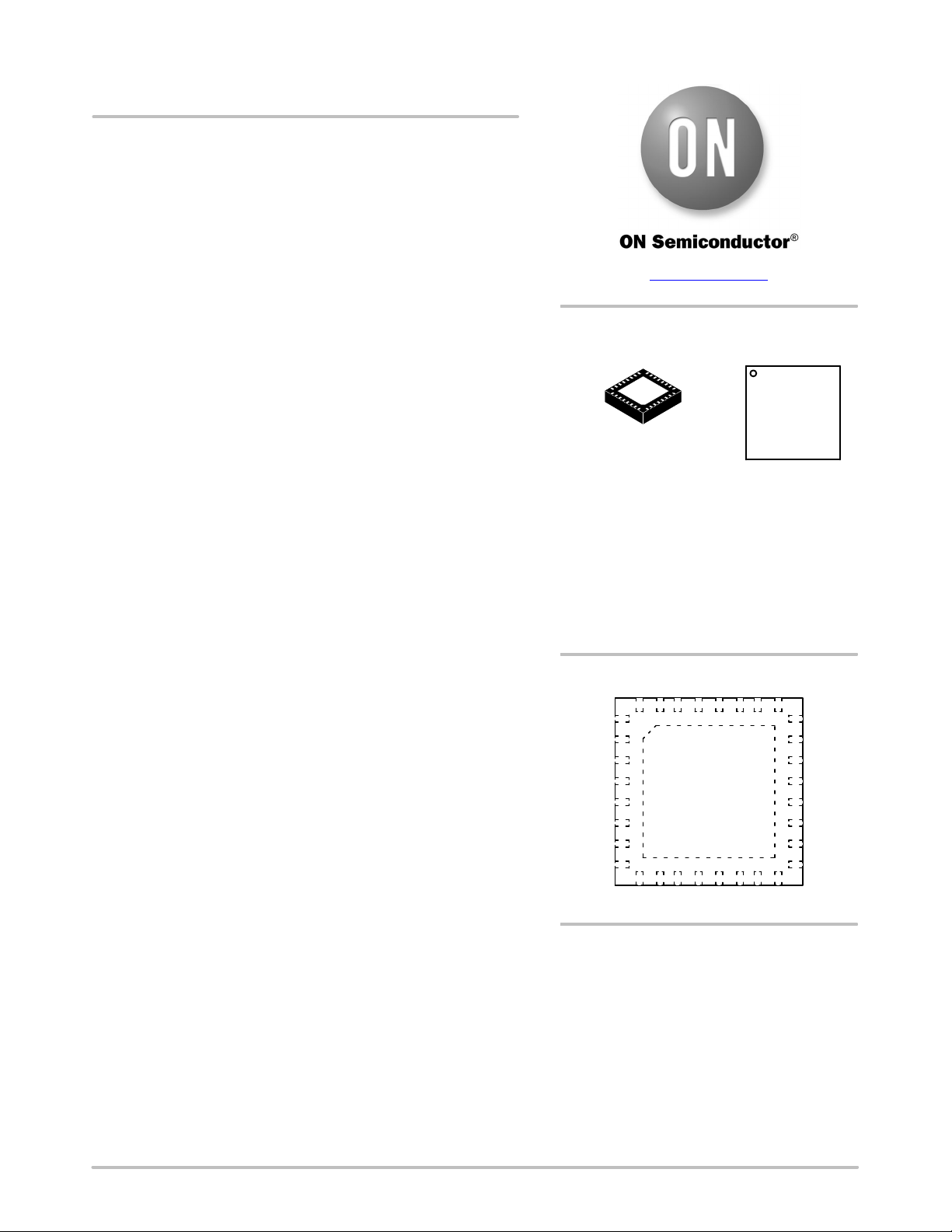
MARKING
DIAGRAM
1
NCP8129x
32
1
LQFN32 5x5, 0.5P
CASE 487AA
NCP8129x = Specific Device Code
x = 5 or 6
A = Assembly Location
WL = Wafer Lot
YY = Year
WW = Work Week
G = Pb−Free Package
(Note: Microdot may be in either location)
= (may or may not be present)
AWLYYWWG
G
Other Features
• 5 mm x 5 mm QFN32 Package
• Operating Temperature: −40°C to 125°C
• Can be Paralleled for Higher Current Applications
• Built−in Insertion Delay for Hotswap Applications
• NCP81295: Latch off for Following Protection Features
NCP81296: Auto−Retry Mode for Following Protection Features
♦ Current−limit after Delay
♦ Fast Short−circuit Protection
♦ Over−Temperature Shutdown
♦ Excessive Soft−start Duration
• Internal Switch Fault Diagnostics
• Low−power Auxiliary Output Voltage
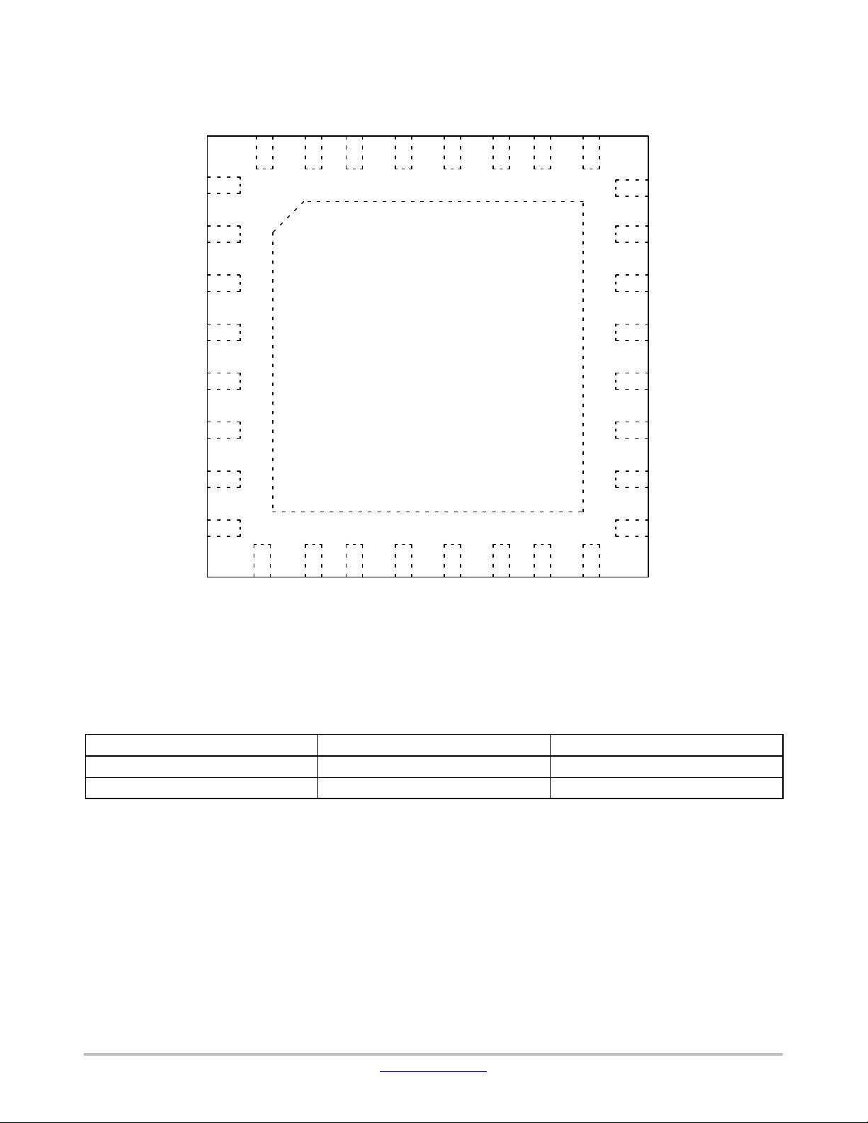
PINOUT
323130
1
2
3
4
5
6
7
8
9
For more details see Figure 1.
29
NCP81295/6
(TOP VIEW)
33
VIN
12
11
10
282726
14
13
25
24
23
22
21
20
19
18
17
16
15
ORDERING INFORMATION
See detailed ordering and shipping information on page 2 of
this data sheet.
© Semiconductor Components Industries, LLC, 2017
April, 2020 − Rev. 12
1 Publication Order Number:
NCP81295/D
NCP81295, NCP81296
†
NC4 1
NC5
D_OC
ON
GOK
NC1
VINF
NC2
VOUT30
VOUT32
32
2
3
4
5
6
7
8
VOUT31
31
30
VOUT29
29
NCP81295 /6
(TOP VIEW)
VOUT28
28
33
VIN
VOUT27
27
VOUT26
26
VOUT25
25
24
23
22
21
20
19
18
17
CLREF
CS
IMON
VDD
GND
SS
VTEMP
GATE
9
VIN9
10
VIN10
11
VIN11
12
VIN12
13
VIN13
14
VIN14
15
VIN15
16
VIN16
Figure 1. Pin Configuration
Ordering Information
Table 1. AVAILABLE DEVICES
Device Package Shipping
NCP81295MNTXG QFN32 2500 / Tape & Reel
NCP81296MNTXG QFN32 2500 / Tape & Reel
†For information on tape and reel specifications, including part orientation and tape sizes, please refer to our Tape and Reel Packaging
Specifications Brochure, BRD8011/D.
www.onsemi.com
2
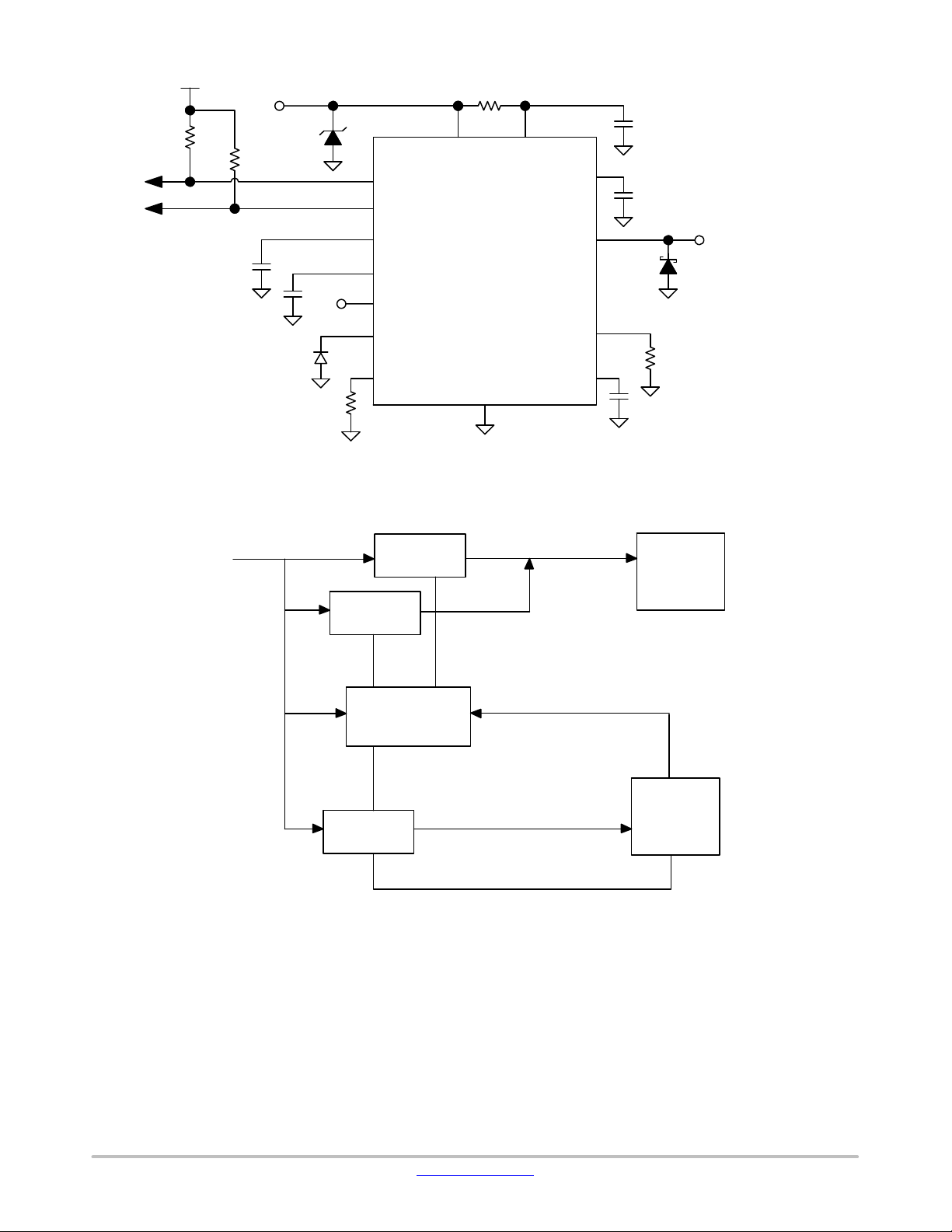
System VIN
NCP81295, NCP81296
VIN VINF
Input
Voltage
GOK
D_OC
ON
VTEMP
IMON
GATE
CLREF
Figure 2.
Main Efuse
Main Efuse
NCP81295/ 6
GND
VOUT
Typical Application
VDD
Fuse−protected
System VIN
CS
SS
Main
System
Power
Main System
E−Fuse
IMON
E−Fuse
Control/
Monitor
PMBSUS Control and
Monitor
Standby
System
Power
E−Fuse
Control/
Monitor
mController
Standby Efuse
E−Fuse
Control/
Monitor
Figure 3. Typical Application Diagram
Standby
System
www.onsemi.com
3
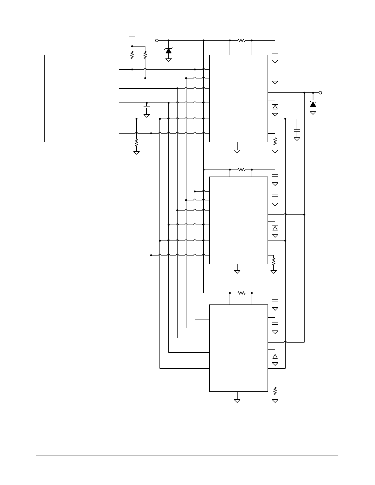
NCP81295, NCP81296
S
VIN
ystem
mController
FAULT IN
OVERCURRENT IN
ENABLE OUT
TEMP MONITOR A/D IN
CURRENT MONITOR A/D IN
CURRENT LIMIT D/A OUT
GOK
D_OC
ON
VTEMP
IMON
CLREF
GOK
D_OC
ON
VTEMP
VIN VINF
NCP81295
VOUT
GATE
GND
VIN VINF
NCP81295
VOUT
GATE
VDD
Fuse−protected
System VIN
SS
CS
VDD
Figure 4.
IMON
CLREF
GOK
D_OC
ON
VTEMP
IMON
CLREF
GND
VIN VINF
NCP81295
GND
SS
CS
VDD
VOUT
GATE
SS
CS
Application Schematic − Parallel Fuse Operation with Controller
www.onsemi.com
4
NCP81295, NCP81296
System VIN
mController
FAULT IN
OVERCURRENT IN
ENABLE OUT
TEMP MONITOR A/D IN
CURRENT LIMIT D/A OUT
CURRENT MONITOR A/D IN
Figure 5. Application Schematic − Single EFuse with Controller
System VIN
VIN
GOK
D_OC
ON
NCP81295/6
VTEMP
CLREF
IMON
GND
VINF
VDD
GATE
VOUT
VIN VINF
GOK
D_OC
NCP81295/6
ON
VTEMP
CLREF
IMON
CS
SS
GND
VDD
GATE
VOUT
CS
SS
Fuse Protected
System VIN
Fuse Protected
System VIN
Figure 6. Application Schematic − Stand−alone Single EFuse
www.onsemi.com
5
NCP81295, NCP81296
S
ystem VIN
VIN VINF
GOK
D_OC
ON
VTEMP
NCP81295
VDD
Fuse−protected
System VIN
VOUT
GATE
IMON
CLREF
GOK
D_OC
ON
VTEMP
IMON
CLREF
SS
CS
GND
VIN VINF
VDD
NCP81295
VOUT
GATE
SS
CS
GND
VIN VINF
GOK
D_OC
ON
VTEMP
IMON
CLREF
Figure 7. Application Schematic − Stand−alone Parallel EFuse
NCP81295
GND
VDD
VOUT
GATE
SS
CS
www.onsemi.com
6
VIN
VINF
VDD
9−16
7
21
VDD_UVR
5V
LDO
CHARGE
PUMP
VINF+2XVDD
EN
NCP81295, NCP81296
SENSEFET
1:5000
ISC
OUTPUT
MONITOR
VDD
VOUT > 90 % VIN
VOUT > 80 % VIN
VOUT > 70 % VIN
VOUT > 40 % VIN
500
PD
5 mA
25−32
-32
19
VOUT
SS
ON
VTEMP
GND
4
18
20
5
VDD
mA
V
VDD
V
SWON
SWOFF
VOUT>90
VOUT>70
DRAIN MON
GATE MON
50 mA
%VIN
%VIN
DIE TEMP
MONITOR
LOGIC
OVERCURRENT
TIMER
VCL_MAX
VCL_HI
VCL_LO
VOUT>80
VOUT>40
%VIN
%VIN
A
IMON
A
CS
VOC_TH(85% CLREF)
VDD
10 mA
22
23
24
3
5
IMON
CS
CLREF
D_OC
GOK
Figure 8. Block Diagram
www.onsemi.com
7

NCP81295, NCP81296
Table 2. PIN DESCRIPTION
Pin No. Symbol Description
1 NC4 No electrical connection internally. May connect to any potential
2 NC5 No electrical connection internally. May connect to any potential
3 D_OC Overcurrent indicator output (open drain). Low indicates the NCP81295 is limiting current. The D_OC
4 ON Enable input and output pulldown resistance control.
5 GOK OK status indicator output (open drain). Low indicates that the NCP81295 was turned off by a fault.
6 NC1 Test pin. Do not connect to this pin. Leave floating
7 VINF
8 NC2 Internal FET sense pin. Do not connect to this pin. Leave floating
9 VIN09 Input of high current output switch
10 VIN10 Input of high current output switch
11 VIN11 Input of high current output switch
12 VIN12 Input of high current output switch
13 VIN13 Input of high current output switch
14 VIN14 Input of high current output switch
15 VIN15 Input of high current output switch
16 VIN16 Input of high current output switch
17 GATE Internal FET gate pin. Connect to the cathode of an anode grounded diode such as BAS16P2T5G. A
18 VTEMP Analog temperature monitor output.
19 SS Soft Start time programming pin. Connect a capacitor to this pin to set the softstart time.
20 GND Ground
21 VDD Linear regulator output
22 IMON Analog current monitor output
23 CS Current sense feedback output (current). Scaling the voltage developed at this pin with a resistor to
24 CLREF Current limit setpoint input for normal operation (after soft−start).
25 VOUT25 Output of high current output switch
26 VOUT26 Output of high current output switch
27 VOUT27 Output of high current output switch
28 VOUT28 Output of high current output switch
29 VOUT29 Output of high current output switch
30 VOUT30 Output of high current output switch
31 VOUT31 Output of high current output switch
32 VOUT32 Output of high current output switch
33 VIN33 Input of high current output switch
output does not report current limiting during soft−start.
Control circuit power supply input. Connect to VIN pins through an RC filter. (1 W / 0.1 mF)
4.7 nF ceramic capacitor is reserved between this pin and GND for NCP81295 to mitigate the oscillation risk when small amount of output capacitance (< 100 mF) or long input/output cable (large L
L
) happens.
OUT
ground makes this also an input for several current limiting functions and overcurrent indicator D_OC.
/
IN
www.onsemi.com
8

NCP81295, NCP81296
Table 3. MAXIMUM RATINGS
Rating Symbol Min Max Unit
Pin Voltage Range (Note 1) Vout enabled VINx, VINF −0.3 20 V
Pin Voltage Range (Note 1) Vout disabled (Note 2) VINx, VINF −0.3 30 V
Pin Voltage Range (Note 1) VOUTx −0.3
−1(<500 ms)
Pin Voltage Range (Note 1) VDD −0.3 6.0 V
Pin Voltage Range (Note 3) All Other Pins −0.3 VDD + 0.3 V
Operating Junction Temperature T
Storage Temperature Range T
Lead Temperature Soldering
Reflow (SMD Styles Only), Pb−Free Versions (Note 4)
Electrostatic Discharge − Charged Device Model ESD
Electrostatic Discharge − Human Body Model ESD
J(max)
STG
T
SLD
CDM
HBM
−55 150 °C
Stresses exceeding those listed in the Maximum Ratings table may damage the device. If any of these limits are exceeded, device functionality
should not be assumed, damage may occur and reliability may be affected.
1. All signals referenced to GND unless noted otherwise.
2. Vout disable is the state of output OFF when internal FET has turned off by disable ON or FAULTs protection.
3. Pin ratings referenced to VDD apply with VDD at any voltage within the VDD Pin Voltage Range.
4. For information, please refer to our Soldering and Mounting Techniques Reference Manual, SOLDERRM/D
20 V
150 °C
260 °C
2.0 kV
2.5 kV
Table 4. THERMAL CHARACTERISTICS
Rating Symbol Value Unit
Thermal Resistance, Junction−to−Ambient (Note 5) R
Thermal Resistance, Junction−to−To p−Case R
Thermal Resistance, Junction−to−Bottom−Case R
Thermal Resistance, Junction−to−Board (Note 6) R
Thermal Resistance, Junction−to−Case (Note 7) R
5. R
is obtained by simulating the device mounted on a 500 mm2, 1−oz Cu pad on a 80 mm x 80 mm, 1.6 mm thick 8−layer FR4 board.
q
JA
value based on hottest board temperature within 1 mm of the package.
6. R
q
JB
7. R
≈ R
q
JC
q
JCT
// R
(Two−Resistor Compact Thermal Model, JESD15−3).
q
JCB
θ
θ
θ
JA
JCT
JCB
θ
JB
θ
JC
30 °C/W
50 °C/W
1.5 °C/W
1.5 °C/W
1.5 °C/W
Table 5. RECOMMENDED OPERATING RANGES
Parameter Symbol Min Max Unit
VIN, VINF Pin Voltage Range 4.5 18 V
Maximum Continuous Output Current I
Peak Output Current I
VDD Output Load Capacitance Range C
VTEMP Output Load Capacitance Range C
Softstart Duration T
CS Load Resistance Range R
CLREF Voltage Range V
Operating Junction Temperature T
AVE
PEAK
VDD
VTEMP
SS
CS
CLREF
J(OP)
2.2 10
0.1
10 100 ms
1.8 4
0.2 1.4 V
−40 125 °C
Functional operation above the stresses listed in the Recommended Operating Ranges is not implied. Extended exposure to stresses beyond
the Recommended Operating Ranges limits may affect device reliability.
50 A
60 A
mF
mF
kW
www.onsemi.com
9

NCP81295, NCP81296
Table 6. ELECTRICAL CHARACTERISTICS (VINx = VINF = 12.0 V, V
= 1 kW, C
R
VTEMP
unless noted otherwise, and are guaranteed by design and characterization through statistical correlation.
Parameter
= 100 nF (unless specified otherwise) Min/Max values are valid for the temperature range −40°C ≤ TA = TJ ≤ 125°C
SS
Symbol Test Conditions Min Typ Max Units
= 3.3 V, C
ON
= 0.1 mF, C
VINF
= 4.7 mF, C
VDD
VTEMP
= 0.1 mF,
VINF INPUT
Quiescent Current
VON > 1.4 V, no load 3.23 5.0 mA
VON > 1.4 V, fault 5.0 mA
VON < 0.8 V 2.38 4.0 mA
VON < 0.8 V, VINF = 16 V 4.0 mA
VDD REGULATOR
VDD Output Voltage
VDD Load Capability I
VDD Current Limit I
V
DD_NL
DDLOAD
DD_CL
VDD Dropout Voltage I
UVLO threshold − rising V
UVLO threshold − falling V
DD_UVR
DD_UVF
I
= 0 mA, VINF = 6 V 4.7 5.09 5.3 V
VDD
VINF = 5.5 V 30 mA
VINF = 12 V and VINF = 6 V 50 70 mA
= 25 mA, VINF = 4.5 V 85 200 mV
VDD
4.1 4.3 4.5 V
3.8 4.0 4.2 V
ON INPUT
Bias Current
Switch ON Threshold V
Switch OFF/ Pulldown Upper
V
Threshold
Pulldown Lower Threshold V
Switch ON Delay Timer t
Switch OFF Delay Time
(Note 8)
ON Current Source Clamp
Voltage
Load Pulldown Delay Timer t
V
ON_CLMP
PD_DEL
Output Pulldown Resistance R
I
ON
SWON
SWOFF
PDOFF
ON
t
OFF
PD
From pin into a 0 V or 1.5 V source 4.0 5.0 6.0
mA
1.33 1.4 1.47 V
1.13 1.2 1.27 V
0.8 V
From ON transitioning above V
start
From ON transitioning below V
pulldown
SWON
SWOFF
to SS
to GATE
0.6 1.0 2.5 ms
1.7
Max pullup voltage of current source 3.0 V
From ON transitioning into the range between
V
and V
SWOFF
V
= 12 V, PD mode = 1 0.77
OUT
PDOFF
2.0 ms
kW
ms
SS PIN
Bias Current
Gain to VOUT AV
SS Pulldown Voltage V
OL_SS
I
SS
SS
From pin into a 0 V or 1 V source 4.62 5.15 5.62
mA
9.6 10 10.4 V/V
0.1 mA into pin during ON delay 22 mV
GOK OUTPUT
Output Low Voltage
Off−state Leakage Current I
V
OL_GOK
LK_GOK
I
= 1 mA 0.1 V
GOK
V
= 5 V 1.0
GOK
mA
Product parametric performance is indicated in the Electrical Characteristics for the listed test conditions, unless otherwise noted. Product
performance may not be indicated by the Electrical Characteristics if operated under different conditions.
8. Guaranteed by design or characterization data. Not tested in production.
www.onsemi.com
10
NCP81295, NCP81296
Table 6. ELECTRICAL CHARACTERISTICS (VINx = VINF = 12.0 V, V
= 1 kW, C
R
VTEMP
unless noted otherwise, and are guaranteed by design and characterization through statistical correlation.
= 100 nF (unless specified otherwise) Min/Max values are valid for the temperature range −40°C ≤ TA = TJ ≤ 125°C
SS
= 3.3 V, C
ON
= 0.1 mF, C
VINF
= 4.7 mF, C
VDD
VTEMP
= 0.1 mF,
Parameter UnitsMaxTypMinTest ConditionsSymbol
IMON/CS OUTPUT
IMON or CS Current
(single EFuse)
Based on 10 mA/A+5 mA
Accuracy (single EFuse) TJ = 0 to 85°C
I
IMON/ICS
TJ = 0 to 85°C
IOUT = 5 A (Note 8) 55
IOUT = 10 A (Note 8) 105
IOUT = 25 A (Note 8) 255
IOUT = 50 A (Note 8) 505
IOUT = 5 A (Note 8) −6 +6 %
mA
mA
mA
mA
IOUT = 10 A (Note 8) −4 +4 %
IOUT = 25 A (Note 8) −4 +4 %
IOUT = 50 A (Note 8) −4 +4 %
IMON or CS Current Source
Clamp Voltage
Pre−Biased Offset Current
Load for Auto−Zero Op−Amp
V
IM_CLMP
V
CS_CLMP
I
AZ_BIAS
/
Max pullup voltage of current source 3.0 V
5.0
mA
CURRENT LIMIT & CLREF PIN
Current Limit Voltage
Current Limit Enact Offset
V
V
Voltage
Current Limit Clamp Voltage
V
V
Max Current Limit Reference
V
Voltage
Response Time (Note 8) t
CL_REG
CLREF Bias Current I
CLREF Current Source
Clamp Voltage
V
CL_CLMP
FET Turn−off Timer t
CL_TH
ENACT
CL_LO
CL_HI
CL_MX
CL
CL_LA
If VCS > VCL_TH current limiting regulation
occurs via gate
0.2 V < V
VOUT < 40% VIN, V
< 1.4 V −70 −24 12 mV
CLREF
> 0.15 V 135 152 165 mV
CLREF
40% VIN < VOUT < 80% VIN
V
> 0.5 V
CLREF
VOUT > 80% VIN, V
VCS > V
until current limiting 200
CLREF
> 1.6 V 1.55 1.6 1.65 V
CLREF
From pin into a 1.2 V source 9.6 10 10.4
95 98 101 %V
CLREF
480 504 520 mV
ms
mA
Max pullup voltage of current source 3.0 V
Delay between current limit detection and FET
250
turn−off (GOK = 0)
ms
D_OC OUTPUT
Overcurrent Threshold
Output Low Voltage V
Off−state Leakage Current I
Delay (rising) (Note 8) VCS < limit until D_OC rising − 1.0
Delay (falling) (Note 8) VCS > limit until D_OC falling − 1.0
VOC_TH If VCS > VOC_TH D_OC pin pulls low 83 86 90 %V
I
OL_DOC
LK_DOC
= 1 mA 0.1 V
DOC
V
= 5 V − 1.0
DOC
CLREF
mA
ms
ms
Product parametric performance is indicated in the Electrical Characteristics for the listed test conditions, unless otherwise noted. Product
performance may not be indicated by the Electrical Characteristics if operated under different conditions.
8. Guaranteed by design or characterization data. Not tested in production.
www.onsemi.com
11

NCP81295, NCP81296
Table 6. ELECTRICAL CHARACTERISTICS (VINx = VINF = 12.0 V, V
= 1 kW, C
R
VTEMP
unless noted otherwise, and are guaranteed by design and characterization through statistical correlation.
= 100 nF (unless specified otherwise) Min/Max values are valid for the temperature range −40°C ≤ TA = TJ ≤ 125°C
SS
= 3.3 V, C
ON
= 0.1 mF, C
VINF
= 4.7 mF, C
VDD
VTEMP
= 0.1 mF,
Parameter UnitsMaxTypMinTest ConditionsSymbol
SHORT CIRCUIT PROTECTION
Current Threshold (Note 8)
I
SC
NCP81295 100 A
NCP81296 80 A
Response Time (Note 8) t
SC
From I
OUT
> I
until gate pulldown 500 ns
LIMSC
VTEMP OUTPUT
Bias Voltage
V
VTEMP25
At 25°C 450 mV
Gain (Note 8) AVTEMP 0°C ≤ TJ ≤ 125°C 10 mV/°C
Load Capability RVTEMP At 25°C 1
Pulldown Current IVTEMP At 25°C 50
kW
mA
THERMAL SHUTDOWN
Temperature Shutdown
(Note 8)
T
TSD
GOK pulls dow 140 °C
OUTPUT SWITCH (FET)
On Resistance
Off−state leakage current I
R
DSon
DSoff
TJ = 25°C 0.65 1.0
VIN = 16 V, VON < 1.2 V, TJ = 25°C 1.0
mW
mA
FAULT detection
Short Threshold VDS_TH Startup postponed if VOUT > VDS_TH at V
V
DS
> V
SWON
transition
ON
VDS Short OK Threshold VDS_OK Startup resumed if VOUT < VDS_OK anytime
88.8 %VIN
68.6 %VIN
after postponed
VGD Short Threshold VDG_TH Startup postponed if VG > VDG_TH at VON >
V
transition
SWON
VGD Short OK Threshold VDG_OK Startup resumed if VG < VDG_OK anytime af-
3.1 V
3.0 V
ter postponed
VG Low Threshold VG_TH Latch/Restart if VGD < VG_TH after t
or t
GATE_FLT
V
Low Threshold V
OUT
Gate Fault Timer (Note 8) t
Startup Timer Failsafe
(Note 8)
OUTL_TH
GATE_FLT
t
SSF_END
Latch/Restart if V
t
SSF_END
Time from VGD < V
SSF_END
completed
t
Time from VON > V
< VOUTL_TH after
OUT
transition after
G_TH
transition,
SWON
Max programmable softstart time
SSF_END
5.4 V
90 %VIN
200 ms
200 ms
AUTO−RETRY (NCP81296)
Auto−Retry Delay
t
DLY_RETRY
Delay from power−down to retry of startup 1000 ms
Product parametric performance is indicated in the Electrical Characteristics for the listed test conditions, unless otherwise noted. Product
performance may not be indicated by the Electrical Characteristics if operated under different conditions.
8. Guaranteed by design or characterization data. Not tested in production.
www.onsemi.com
12

NCP81295, NCP81296
Test Conditions: Vin = 12 V, Rcs = 2 kW, Css = 200 nF, R
600
500
400
300
Ics (mA)
200
100
0
6050403020100
LOAD CURRENT (A) LOAD CURRENT (A)
600
500
400
300
Imon (mA)
200
100
0
Figure 9. Ics vs. Load Current Figure 10. Imon vs. Load Current
600
500
400
50 A
600
500
400
CLREF
= 121 kW, R
IMON
= 2 kW
6050403020100
50 A
TYPICAL CHARACTERISTICS
300
Ics (mA)R
200
100
1.0
0.9
0.8
0.7
0.6
(mW)
0.5
0.4
DS(on)
0.3
0.2
0.1
0
TEMPERATURE (°C) TEMPERATURE (°C)
Figure 11. Ics vs. Temperature Figure 12. Imon vs. Temperature
0
0 120 140
TEMPERATURE (°C) TEMPERATURE (°C)
Figure 13. Output Switch R
Temperature
30 A
DS(on)
1251007550250−25−50
10080604020−20−40−60
@ 22 A vs.
300
Imon (mA)
200
100
0
1600
1400
1200
1000
800
Vtemp (mV)
600
400
200
0
Figure 14. Vtemp vs. Temperature (no load)
30 A
1251007550250−25−50
150150
20 80 140
12010060400−20−40−60
www.onsemi.com
13

NCP81295, NCP81296
Test Conditions: Vin = 12 V, Rcs = 2 kW, Css = 200 nF, R
0
−1
−2
−3
−4
OFF−STATE LEAKAGE (mA)
−5
−6
TEMPERATURE (°C)
40 120 140
1008060200−20−40−60
2500
2000
1500
1000
POWER LOSS (mW)
500
0
Figure 15. Output Switch Off−state Leakage
vs. Temperature
1000
100
10
1
R
Limit
0.1
DS(ON)
Single Pulse
R
= 24.8 °C/W
q
JA
T
= 25°C
A
VDS, DRAIN−SOURCE VOLTAGE (V)
Dotted Lines: Measured SOA
Solid Lines: Calculated SOA
10.1
, DRAIN CURRENT (A)
D
I
0.01
Figure 17. Internal FET’s Safe Operating Area (SOA)
CLREF
= 121 kW, R
OUTPUT CURRENT (A)
= 2 kW
IMON
30 50
Power Loss
4020100
Figure 16. Power Loss vs. Load Current
100 ms
250 ms
1 ms
10 ms
100 ms
1 s
10 s
10
20
60
TYPICAL CHARACTERISTICS
100k
10k
1k
100
POWER (W)
10
1
0.00001 0.0001 0.001 0.01 0.1 1.0 100 1k10
TA = 25°C
TA = 85°C
PULSE WIDTH (s)
Figure 18. Single Pulse Power Rating (10 ms −
1000 s, Junction−to−Ambient, Note 4)
250
200
150
100
POWER (W)
50
0
0.01 0.10.2 0.3 0.90.80.70.4 0.5 0.6
www.onsemi.com
14
TA = 25°C
TA = 85°C
PULSE WIDTH (s)
Figure 19. Single Pulse Power Rating (10 ms −
100 ms, Junction−to−Ambient, Note 4)
NCP81295, NCP81296
Test Conditions: Vin = 12 V, Rcs = 2 kW, Css = 200 nF, R
Figure 20. Start Up by VIN (Iout = 0 A) Figure 21. Shut Down by VIN (Iout = 0 A)
CLREF
= 121 kW, R
IMON
= 2 kW
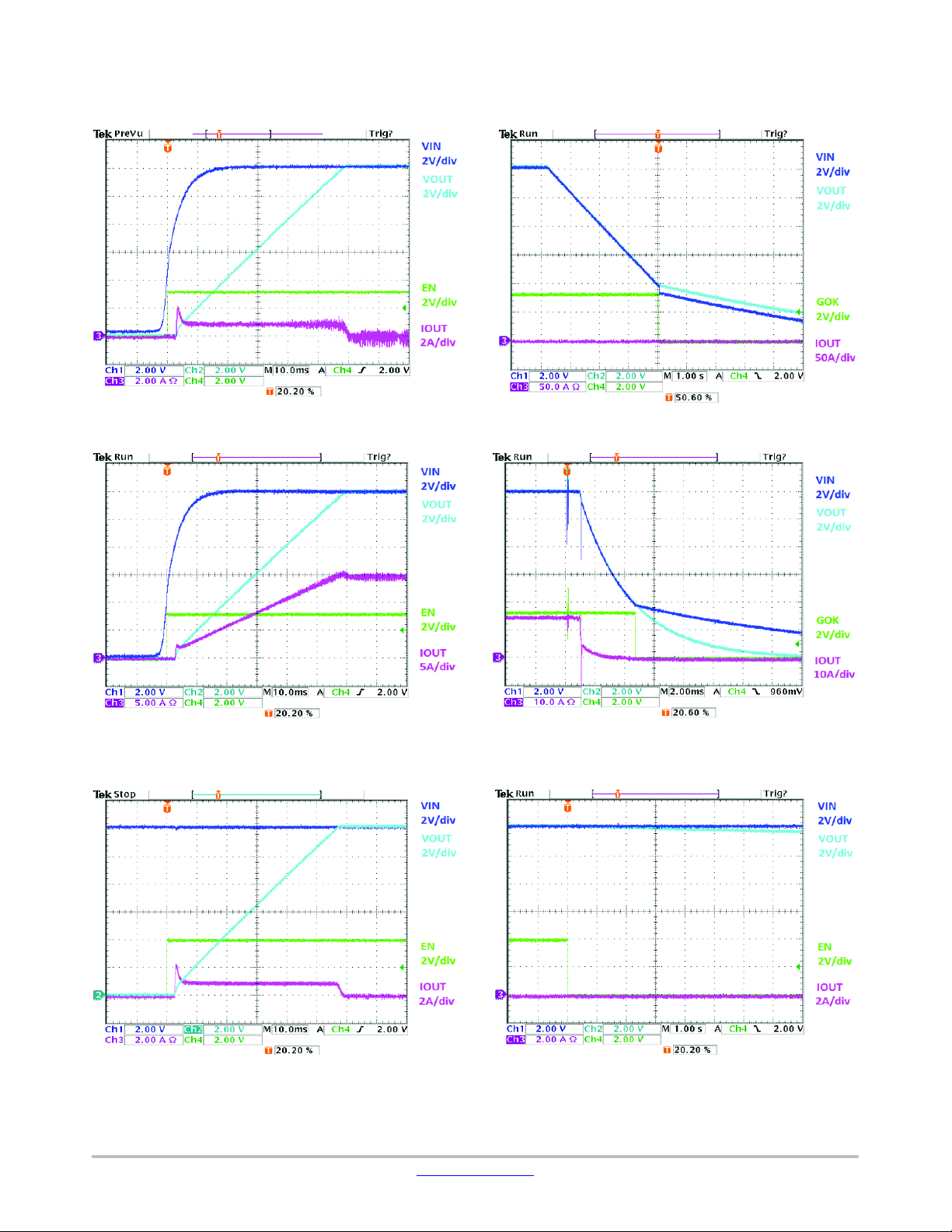
TYPICAL CHARACTERISTICS
Figure 22. Start Up by VIN (Iout = 15 A) Figure 23. Shut Down by VIN (Iout = 15 A)
Figure 24. Start Up by EN (Iout = 0 A) Figure 25. Shut Down by EN (Iout = 0 A)
www.onsemi.com
15
NCP81295, NCP81296
Test Conditions: Vin = 12 V, Rcs = 2 kW, Css = 200 nF, R
Figure 26. Start Up by EN (Iout = 15 A) Figure 27. Shut Down by EN (Iout = 15 A)
CLREF
= 121 kW, R
IMON
= 2 kW
TYPICAL CHARACTERISTICS
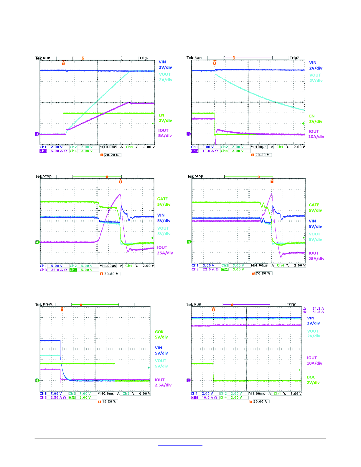
Figure 28. Short Circuit during Normal
Operation (Iout = 0 A)
Figure 30. Short FET’s Gate During Normal
Operation (Iout = 2.5 A)
Figure 29. Short Circuit during Normal
Operation (Iout = 50 A)
Figure 31. DOC Index for Current Limit during
Normal Operation (Iout = 51.8 A)
www.onsemi.com
16
NCP81295, NCP81296
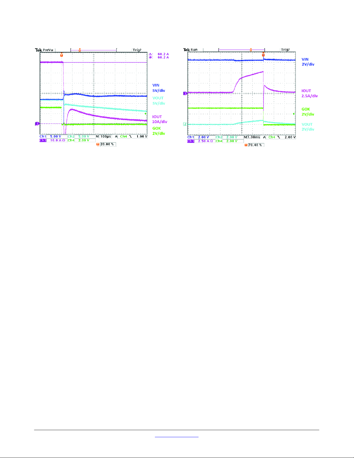
Test Conditions: Vin = 12 V, Rcs = 2 kW, Css = 200 nF, R
Figure 32. OCP during Normal
Operation(Iout=60.2A)
TYPICAL CHARACTERISTICS
CLREF
Figure 33. OCP during Power Up by Enable
= 121 kW, R
IMON
= 2 kW
www.onsemi.com
17
NCP81295, NCP81296
General Information
The NCP81295/6 is an N−channel MOSFET
co−packaged with a smart hotswap controller. It is suited for
high−side current limiting and fusing in hot−swap
applications. It can be used either alone, or in a paralell
configuration for higher current applications.
VDD Output (Auxiliary Regulated Supply)
An internal linear regulator draws current from the VINF
pin to produce and regulate voltage at the VDD pin. This
auxiliary output supply is current−limited to I
DD_CL
. A
ceramic capacitor in the range of 2.2 mF to 10 mF must be
placed between the VDD and GND pins, as close to the
NCP81295/6 as possible. The voltage difference between
VIN and VINF pin voltage should be within 0.4 V for better
CS/IMON performance. Small time constant R/C filter such
as 1 W/0.1 mF on the VINF pin is recommended.
ON Input (Device Enable)
When the ON pin voltage (VON) is higher than V
SWON
and no undervoltage (UVLO) or output switch faults are
present, the output switch turns on. When V
V
and V
, the output switch is off. If VON is between V
SWOFF
for longer than t
SWOFF
PD_DEL
, the output switches
off, and a pulldown resistance to ground, of R
is lower than
ON
, is applied
PD
PDOFF
to VOUT. In other words, there is behavior as follows:
• When V
• When 0.8 V < V
< 0.8 V, FET turns off.
ON
< 1.2 V, VOUT will discharge with
ON
15 mA.
• When V
> 1.2 V, FET turns on.
ON
For standalone applications, the ON pin sources current
ION, which can be used to delay output switch turn−on for
some time after the appearance of input voltage by
connecting a capacitor from the ON pin to ground.
A bi−level control signal driving to ground can be biased
up with a resistive divider to produce ON input levels
between V
PDOFF
< VON < V
and VON > V
SWON
SWON
in
order to always apply the output pulldown when the output
switch is off.
SS Output (Soft−Start)
When the output switch first turns on, it does so in a
controlled manner. The output voltage (VOUT) follows the
voltage at the SS pin, produced by current I
into a capacitor
SS
from SS to ground. The duration of soft−start can be
programmed by selection of the capacitor value. In parallel
fuse applications, the SS pins of all fuses should be shorted
together to one shared SS capacitor. Internal soft−start load
balancing circuity will ensure the soft−start current is shared
between paralleled devices, so as not to stress one device
more than another or hit a soft start−current limit.
The soft−start capacitor value can be calculated by:
C
SS
= (t
SS
* I
* AVSS)/VIN (where t
SS
soft−start time). The recommended range of t
is the target
SS
is 10 −
SS
100 ms (see Table 5).
The typical C
values for different tSS are listed below:
SS
tSS (ms) CSS (nF) tSS (ms) CSS (nF)
10 47 60 270
20 82 70 330
30 120 80 330
40 180 90 470
50 220 100 470
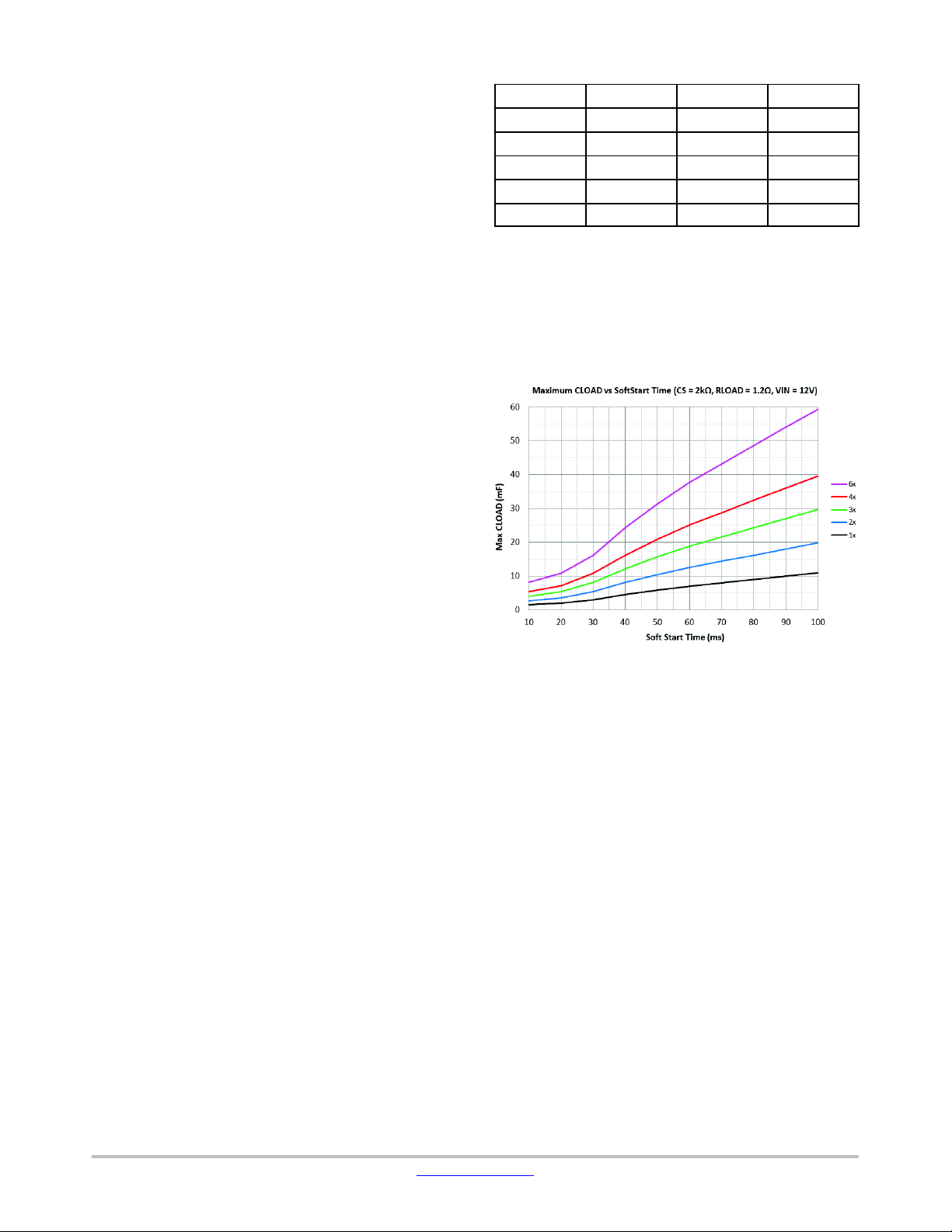
The maximum load capacitor value NCP81295/6 can
power up depends on the device soft−start time. When
=12V, RCS = 2 kW, R
V
IN
= 2.4 W, their relationship
LOAD
for different paralleled operations are shown as below chart
(above line device shuts down safely due to protection,
below line device powers up successfully without trigger
protection):
,
GOK Output (Gate OK)
The GOK pin is an open−drain output that is pulled low to
report the fault under the following conditions:
• V
voltage is below UVLO voltage at any time.
DD
• V
disabled and V
ON
DS_OK
is false
(indicates a short from VIN to VOUT).
• V
disabled and V
ON
DG_OK
is false
(indicates a short from GATE to VIN).
• V
enabled and V
ON
SS_OK
is false at t
SSF_END
(indicates VOUT < 90% after soft−start completes
− FET latches off for NCP81295/auto−retries for
NCP81296).
• V
ON
enabled and V
is below V
G
G_TH
at t
(indicates leakage on GATE in startup – FET latches off
for NCP81295/auto−retries for NCP81296).
• V
ON
enabled and V
is below V
G
G_TH
after t
(indicates leakage on GATE during normal operation
– FET latches off for NCP81295/auto−retries for
NCP81296).
• V
enabled and a current−limiting condition lasts
ON
longer than t
OC_LA
(FET latches off for NCP81295/auto−retries for
NCP81296).
SSF_END
GATE_FLT
www.onsemi.com
18

NCP81295, NCP81296
• V
enabled and device temperature is above T
ON
TSD
(indicates an over−temperature is detected − FET
latches off for NCP81295/auto−retries for NCP81296).
Usually GOK can’t be used as power good to indicate the
output voltage is in the normal range. Bringing VDD below
the UVLO voltage is required to release a latching condition.
IMON Output (Current Monitor)
The IMON pin sources a current that is A
times the VOUT output current and plus I
AZ_BIAS
IMON
(10 mA/A)
. A resistor
connected from the IMON pin to ground can be used to
monitor current information as a voltage up to V
IM_CLMP
. A
capacitor of any value in parallel with the IMON resistor can
be used to low−pass filter the IMON signal without affecting
any internal operation of the device.
CLREF Pin (Current Limit and Over−Current Reference)
The CLREF pin voltage determines the current−limit
regulation point and over−current indication point via its
interaction with the CS pin voltage. The CLREF voltage can
be applied by an external source, such as a hot−swap
controller or D−to−A converter, or developed across a
programming resistor to ground by the CLREF bias current,
I
. The recommended range of CLREF voltage is 0.2 −
CL
1.4 V (see Table 5).
CS Input/Output (Current Set)
The CS pin is both an input and an output. The CS pin
sources a current that is A
current and plus I
AZ_BIAS
(10 mA/A) times the VOUT
CS
. This produces a voltage on the CS
pin that is the product of the CS pin current and an external
CS pin resistance to ground.
The voltage generated on V
determines the D_OC
CS
over−current indicator trip point and the current−limit
regulation point, via its interaction with the voltage on
CLREF pin.
When the voltage on the CS pin is higher than V
OC_TH
D_OC is pulled low. If the CS pin voltage drops below
V
, the D_OC pin is released to and gets pulled high by
OC_TH
the external pullup resistor. D_OC transitions based on the
following formula:
V
The V
OC_TH)VENACT
R
I
+
OUT
trip point is based on a percentage of V
OC_TH
CS
10 m
* I
AZ_BIAS
(eq. 1)
CLREF
(86%).
During normal operation (V
t
(V
), if the voltage on the CS pin is above V
SS_END
is clamped at V
CL_TH
CL_MX
ON
> V
if V
CL_TH
for longer than
SWON
> V
CL_MX
CL_TH
), then
the gate voltage of the FET is modulated to limit current into
the output based on the following formula:
V
The V
CL_TH)VENACT
R
I
+
OUT
regulation point is equal to V
CL_TH
CS
10 m
* I
AZ_BIAS
CLREF
(eq. 2)
.
During startup (V
ON
> V
SWON
for less than t
current limit reference voltage is clamped according to the
following:
• When VOUT < 40% of VIN, V
V
(whichever is lower).
CLREF
CL_TH
= V
• When VOUT is between 40% and 80% of VIN,
CL_TH
= V
V
• When VOUT exceeds 80% of VIN, V
or V
If a current limiting condition exists anytime for a
continuous duration > t
(NCP81295) or restarts (NCP81296).
The CS pin must have no capacitive loading other than
parasitic device/board capacitance to function correctly. The
recommended range of R
CS AMP OFFSET BIAS
NCP81295/6 use an auto−zero Op−Amp with low input
offset to sense current in FET with high−accuracy, and an
pre−biased offset current load, I
Op−Amp to always keep it to maintain this low input offset
(<100 mV). The internal IMON and CS current source
follow below relationship:
and
For typical 5 mA I
in I
OUT
D_OC Output (Over−current Indicator)
The D_OC pin is an open−drain output that indicates
when an over−current condition exists after soft−start is
,
complete. When the voltage on the CS pin is higher than
V
OC_TH
V
OC_TH
an external pullup resistor.
VTEMP Output (Temperature Indicator)
VTEMP is a voltage output proportional to device
temperature, with an offset voltage. The VTEMP output can
source much more current than it can sink, so that if multiple
VTEMP outputs are connected together, the voltage of all
VTEMP outputs will be driven to the voltage produced by
the hottest NCP81295/6. A 100 nF capacitor or greater must
be connected from the VTEMP pin to ground.
CLREF
sense.
, D_OC is pulled low. If output current drops below
, the D_OC pin is released and gets pulled high by
CL_HI
or V
CLREF
(whichever is lower).
, then the device latches off
CL_LA
is 1.8 − 4kW (see Table 5).
CS
ICS* I
I
+
OUT
I
+
OUT
AZ_BIAS
10 m
I
* I
MON
10 m
, there has 0.5 A positive off−set
(whichever is lower).
CL_TH
AZ_BIAS
AZ_BIAS
AZ_BIAS
is need for this
SS_END
CL_LO
= V
), the
or
CL_MX
(eq. 3)
(eq. 4)
www.onsemi.com
19

NCP81295, NCP81296
Auto−Retry Restart (NCP81296)
Under certain fault conditions, the FET is turned off and
another soft−start procedure takes place. Between the fault
and the new soft−start, there is a delay of t
DLY_RETRY
. The
protection features that use this hiccup mode restart are:
• Over−Current
• Short−Circuit Detection
• Over−Temperature
• Excessive Soft−Start Duration
• Gate Leakage
Protection Features
For the following protection features, the FET either
latches off (NCP81295) or the FET turns off and initiates a
restart (NCP81296), unless noted otherwise.
Excessive Current Limiting
If a current limiting condition exists anytime for a
continuous duration > t
Excessive Soft−Start Duration
If VOUT < V
OUTL_TH
FET latches/restarts.
Short Circuit Detection
If switch current exceeds ISC, the device reacts within tSC,
and the FET latches/restarts. The short−circuit current
monitor is independent of CS, CLREF, IMON and current
limit setting (cannot be changed externally).
Over−Temperature Shutdown
If the FET controller temperature > T
latches/restarts.
, then the FET latches/restarts.
CL_LA
when t
SSF_END
expires, then the
, then the FET
TSD
• VIN to VOUT short, non−latching/non−auto−retry
condition. If the device is disabled and
VOUT > V
then GOK is pulled low and the
DS_TH
device is prevented from powering up. The device is
allowed to power up once VOUT < V
DS_OK
.
• GATE to VIN short, non−latching/non−auto−retry
condition. If the device is disabled and
GATE (Pin 8) > V
, then GOK is pulled low and
DG_TH
device is prevented from powering up. The device
allowed to power up once GATE < V
DG_OK.
• GATE leakage − startup.
If (GATE – VINF) < V
G_TH
at t
SSF_END
pulled low and FET latches/restarts.
, then GOK is
• GATE leakage − normal operation.
If (GATE – VINF) < V
G_TH
for t
GATE_FLT
the soft−start timer completes, then GOK is pulled low
and device latches/restarts.
FET SOA Limits
In−built timed current limits and fault−monitoring circuits
ensure the copackaged FET is always kept within SOA
limits.
Multiple Fuse Power Up
When multiple NPC81295 are paralleled together as
shown in Figure 4, the NPC81295s will turn on together.
Keeping the current through each switch within 1 A (typical)
helps to prevent overstress on each switching during
soft−start.
Due to NCP81296 is featured by Auto−Retry Mode
protection, please follow the below reference schematic
of NCP81296 for paralleled operation.
time after
FET Fault Detection
The device contains various FET monitoring circuits:
www.onsemi.com
20
NCP81295, NCP81296
When paralleled multiple NPC81295 encounter fault, the system can recover the E−fuse by resetting their VDD with below
buffer and reset circuit.
www.onsemi.com
21
NCP81295, NCP81296
22nF
22nF
www.onsemi.com
22

MECHANICAL CASE OUTLINE
PACKAGE DIMENSIONS
32
1
SCALE 2:1
A
B
E
(A3)
A
A1
C
K
17
E2
24
25
b
32X
M
0.10 BC
M
0.05 C
32X
0.63
PIN ONE
REFERENCE
0.10 C
0.10 C
0.05 C
NOTE 4
DETAIL C
0.10
DETAIL A
32X
L
D
C
TOP VIEW
DETAIL B
SIDE VIEW
D2
9
1
32
e
e/2
BOTTOM VIEW
RECOMMENDED
SOLDERING FOOTPRINT*
5.30
3.60
LQFN32 5x5, 0.5P
CASE 487AA
ISSUE A
DETAIL A
ALTERNATE
CONSTRUCTION
A1
CONSTRUCTION
SEATING
PLANE
L2
A
NOTE 3
L
DETAIL B
ALTERNATE
DETAIL C
4 PLACES
NOTES:
1. DIMENSIONING AND TOLERANCING PER
ASME Y14.5M, 1994.
2. CONTROLLING DIMENSION: MILLIMETERS.
3. DIMENSION b APPLIES TO PLATED
TERMINAL AND IS MEASURED BETWEEN
0.15 AND 0.30 MM FROM THE TERMINAL TIP.
4. COPLANARITY APPLIES TO THE EXPOSED
PAD AS WELL AS THE TERMINALS.
MILLIMETERS
DIM MIN MAX
A3
L2
A 1.20 1.40
A1 −−− 0.05
A3 0.20 REF
b 0.18 0.30
D 5.00 BSC
D2 3.30 3.50
E 5.00 BSC
E2
3.30 3.50
e 0.50 BSC
L 0.30 0.50
L2 0.13 REF
GENERIC
MARKING DIAGRAM*
1
XXXXXXXX
XXXXXXXX
AWLYYWWG
G
XXXXX = Specific Device Code
A = Assembly Location
WL = Wafer Lot
YY = Year
WW = Work Week
G = Pb−Free Package
(Note: Microdot may be in either location)
*This information is generic. Please refer
to device data sheet for actual part
marking.
Pb−Free indicator, “G” or microdot “ G”,
may or may not be present. Some products may not follow the Generic Marking.
DATE 03 OCT 2017
3.60
0.50
PITCH
DIMENSIONS: MILLIMETERS
5.30
32X
0.30
*For additional information on our Pb−Free strategy and soldering
details, please download the ON Semiconductor Soldering and
Mounting Techniques Reference Manual, SOLDERRM/D.
DOCUMENT NUMBER:
DESCRIPTION:
ON Semiconductor and are trademarks of Semiconductor Components Industries, LLC dba ON Semiconductor or its subsidiaries in the United States and/or other countries.
ON Semiconductor reserves the right to make changes without further notice to any products herein. ON Semiconductor makes no warranty, representation or guarantee regarding
the suitability of its products for any particular purpose, nor does ON Semiconductor assume any liability arising out of the application or use of any product or circuit, and specifically
disclaims any and all liability, including without limitation special, consequential or incidental damages. ON Semiconductor does not convey any license under its patent rights nor the
rights of others.
© Semiconductor Components Industries, LLC, 2019
98AON11454G
LQFN32, 5x5, 0.5P
Electronic versions are uncontrolled except when accessed directly from the Document Repository.
Printed versions are uncontrolled except when stamped “CONTROLLED COPY” in red.
PAGE 1 OF 1
www.onsemi.com

ON Semiconductor and are trademarks of Semiconductor Components Industries, LLC dba ON Semiconductor or its subsidiaries in the United States and/or other countries.
ON Semiconductor owns the rights to a number of patents, trademarks, copyrights, trade secrets, and other intellectual property. A listing of ON Semiconductor’s product/patent
coverage may be accessed at www.onsemi.com/site/pdf/Patent−Marking.pdf
ON Semiconductor makes no warranty, representation or guarantee regarding the suitability of its products for any particular purpose, nor does ON Semiconductor assume any liability
arising out of the application or use of any product or circuit, and specifically disclaims any and all liability, including without limitation special, consequential or incidental damages.
Buyer is responsible for its products and applications using ON Semiconductor products, including compliance with all laws, regulations and safety requirements or standards,
regardless of any support or applications information provided by ON Semiconductor. “Typical” parameters which may be provided in ON Semiconductor data sheets and/or
specifications can and do vary in different applications and actual performance may vary over time. All operating parameters, including “Typicals” must be validated for each customer
application by customer’s technical experts. ON Semiconductor does not convey any license under its patent rights nor the rights of others. ON Semiconductor products are not
designed, intended, or authorized for use as a critical component in life support systems or any FDA Class 3 medical devices or medical devices with a same or similar classification
in a foreign jurisdiction or any devices intended for implantation in the human body. Should Buyer purchase or use ON Semiconductor products for any such unintended or unauthorized
application, Buyer shall indemnify and hold ON Semiconductor and its officers, employees, subsidiaries, affiliates, and distributors harmless against all claims, costs, damages, and
expenses, and reasonable attorney fees arising out of, directly or indirectly, any claim of personal injury or death associated with such unintended or unauthorized use, even if such
claim alleges that ON Semiconductor was negligent regarding the design or manufacture of the part. ON Semiconductor is an Equal Opportunity/Affirmative Action Employer. This
literature is subject to all applicable copyright laws and is not for resale in any manner.
. ON Semiconductor reserves the right to make changes without further notice to any products herein.
PUBLICATION ORDERING INFORMATION
LITERATURE FULFILLMENT:
Email Requests to: orderlit@onsemi.com
ON Semiconductor Website: www.onsemi.com
TECHNICAL SUPPORT
North American Technical Support:
Voice Mail: 1 800−282−9855 Toll Free USA/Canada
Phone: 011 421 33 790 2910
Europe, Middle East and Africa Technical Support:
Phone: 00421 33 790 2910
For additional information, please contact your local Sales Representative
◊
www.onsemi.com
1
 Loading...