

High Speed Half-Bridge
Driver for GaN Power
Switches
NCP51820
The NCP51820 high−speed, gate driver is designed to meet the
stringent requirements of driving enhancement mode (e−mode), high
electron mobility transistor (HEMT) and gate injection transistor
(GIT), gallium nitrade (GaN) power switches in off−line, half−bridge
power topologies. The NCP51820 offers short and matched
propagation delays with advanced level shift technology providing
−3.5 V to +650 V (typical) common mode voltage range for the
high−side drive and −3.5 V to +3.5 V common mode voltage range for
the low−side drive. In addition, the device provides stable dV/dt
operation rated up to 200 V/ns for both driver output stages in high
speed switching applications.
To fully protect the gate of the GaN power transistor against
excessive voltage stress, both drive stages employ a dedicated voltage
regulator to accurately maintain the gate−source drive signal
amplitude. The circuit actively regulates the driver’s bias rails and thus
protects against potential gate−source over−voltage under various
operating conditions.
The NCP51820 offers important protection functions such as
independent under−voltage lockout (UVLO), monitoring VDD bias
voltage and VDDH and VDDL driver bias and thermal shutdown
based on die junction temperature of the device. Programmable
dead−time control can be configured to prevent cross−conduction.
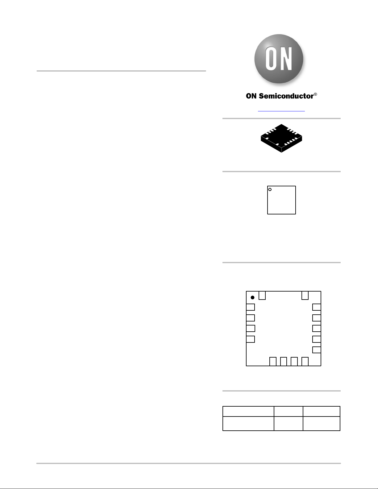
www.onsemi.com
QFN15 4x4, 0.5P
CASE 485FN
MARKING DIAGRAM
51820A
ALYW G
G
51820A = Specific Device Code
A = Assembly Site
L = Wafer Lot Number
YW = Assembly Start Week
G = Pb−Free Package
(Note: Microdot may be in either location)
Features
• 650 V, Integrated High−Side and Low−Side Gate Drivers
• UVLO Protections for VDD High and Low−Side Drivers
• Dual TTL Compatible Schmitt Trigger Inputs
• Split Output Allows Independent Turn−ON/Turn−OFF Adjustment
• Source Capability: 1 A; Sink Capability: 2 A
• Separated HO and LO Driver Output Stages
• 1 ns Rise and Fall Times Optimized for GaN Devices
• SW and PGND: Negative Voltage Transient up to 3.5 V
• 200 V/ns dV/dt Rating for all SW and PGND Referenced Circuitry
• Maximum Propagation Delay of Less Than 50 ns
• Matched Propagation Delays to Less Than 5 ns
• User Programmable Dead−Time Control
• Thermal Shutdown (TSD)
Typical Applications
• Driving GaN Power Transistors used in Full or Half−Bridge, LLC,
Active Clamp Flyback or Forward, Totem Pole PFC and
Synchronous Rectifier Topologies
• Industrial Inverters and Motor Drives
• AC to DC Converters
PIN ASSIGNMENT
VBST
15
VDDH
HOSRC
HOSNK
NCP51820AMNTWG QFN15
†For information on tape and reel specifications,
including part orientation and tape sizes, please
refer to our Tape and Reel Packaging Specifications
Brochure, BRD8011/D.
1
2
3
SW
4
ORDERING INFORMATION
Device Package Shipping
NCP51820
(Top View)
5
6
VDDL
LOSRC
(Pb−Free)
VDD8
14
7
PGND
LOSNK
13
EN
HIN
12
LIN
11
SGND
10
DT
9
4000 / Tape
& Reel
†
© Semiconductor Components Industries, LLC, 2019
February, 2021 − Rev. 3
1 Publication Order Number:
NCP51820/D
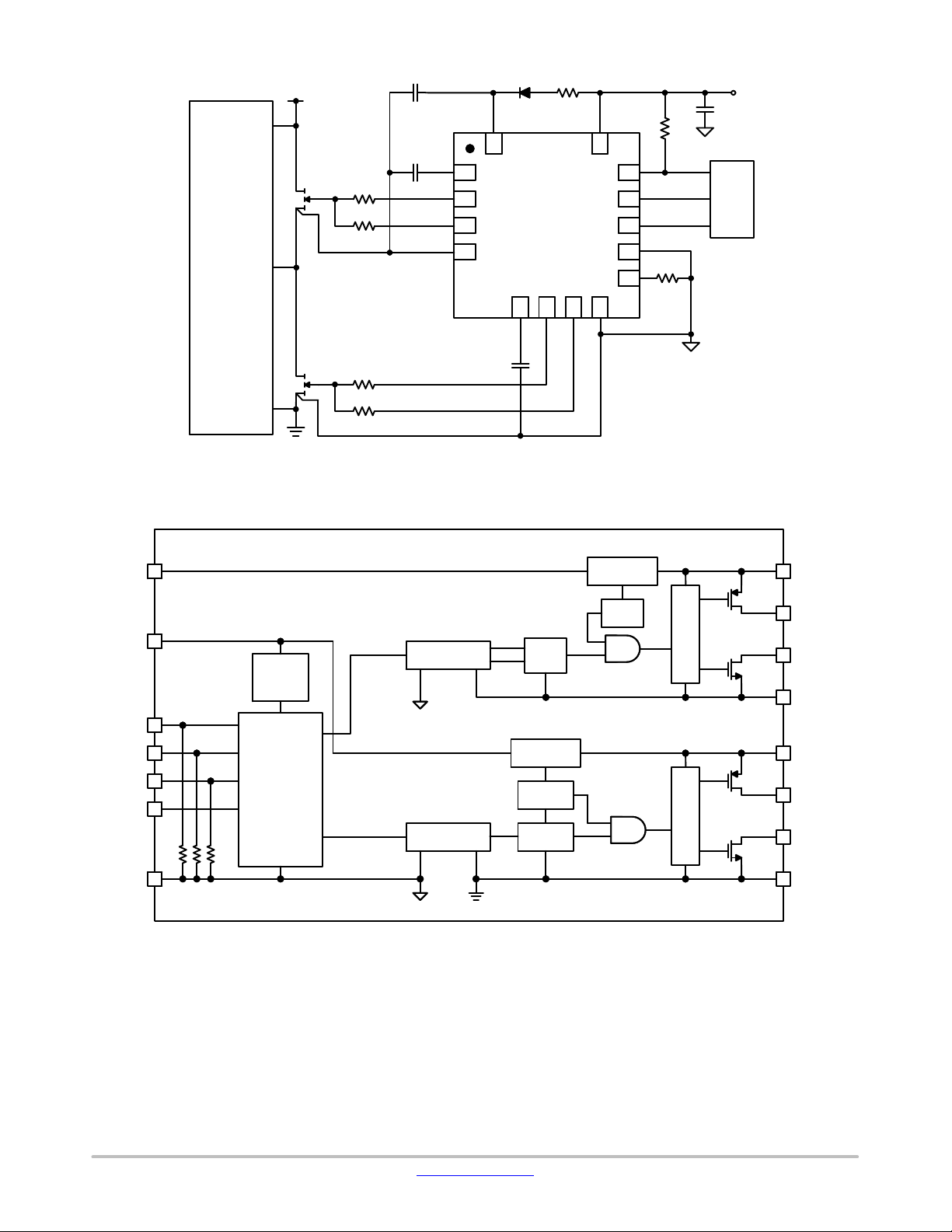
NCP51820
VDDVIN
VBST
POWER
STAGE
VBST
15
VDDH
1
HOSRC
2
HOSNK
SW
3
4
NCP51820
(Top View)
5
VDDL
6
LOSRC
7
LOSNK
Figure 1. Typical Application Schematic
VDD
14
13
12
11
10
9
8
PGND
VDDH
REGULATOR
EN
HIN
LIN
SGND
DT
PWM
mC
or
DSP
VDDH
VDD
EN
HIN
LIN
DT
SGND
VDD
UVLO
8.5V/8V
(ON/OFF)
SCHMITT
TRIGGER INPUT
SHOOT THOUGH
PREVENTION
CYCLE−By−
CYCLE EDGE
TRIGGERED
SHUTDOWN
DEAD−TIME
MODE CONTROL
HO
LEVEL SHIFTER
LO
LEVEL SHIFTER
S
Q
R
VDDL
REGULATOR
VDDL
UVLO
DELAY
Figure 2. Internal Block Diagram
VDDH
UVLO
DRIVER
DRIVER
HOSRC
HOSNK
SW
VDDL
LOSRC
LOSNK
PGND
www.onsemi.com
2
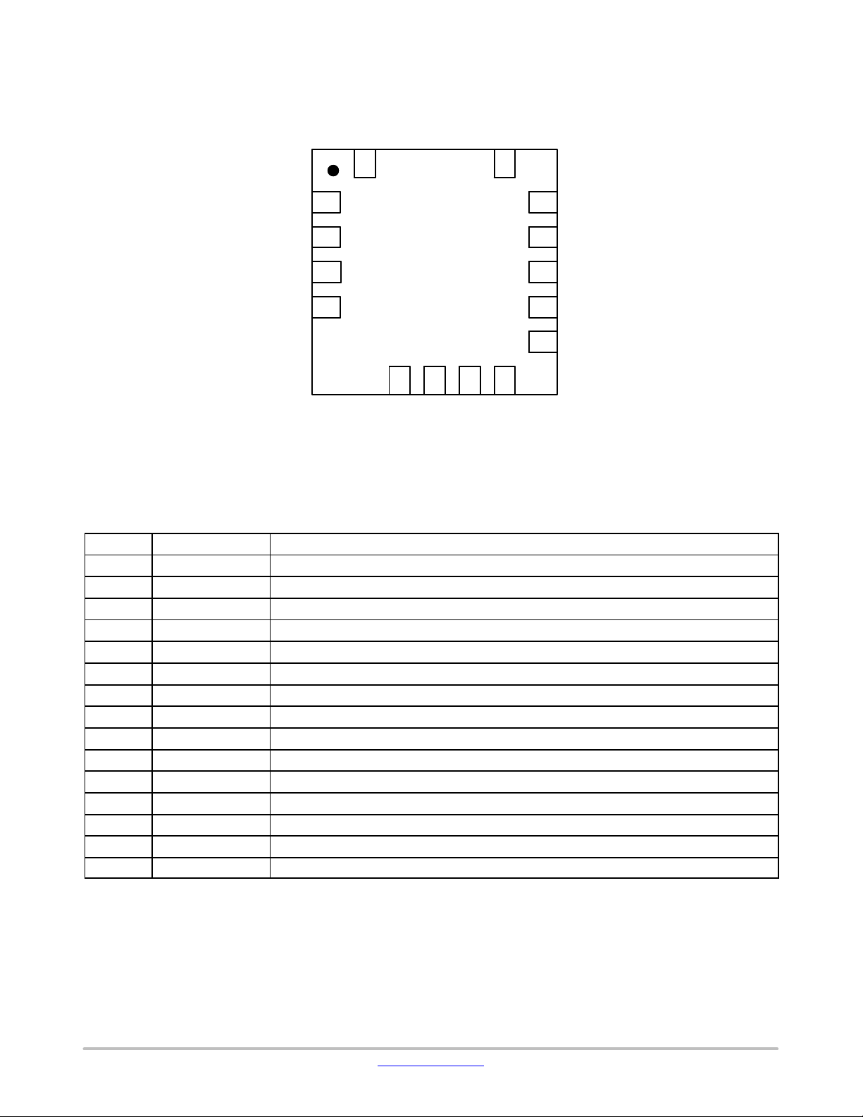
PIN CONNECTIONS
NCP51820
VDDH
HOSRC
HOSNK
SW
VBST
15
1
2
3
4
NCP51820
(Top View)
5
6
VDDL
LOSRC
7
LOSNK
VDD8
14
PGND
Figure 3. Pin Assignments – 15 Lead QFN (Top View)
PIN DESCRIPTION
Pin No. Name Description
1 VDDH High−side driver positive bias voltage output
2 HOSRC High−side driver sourcing output
3 HOSNK High−side driver sinking output
4 SW Switch−node / high−side driver return
5 VDDL Low−side driver positive bias voltage output
6 LOSRC Low−side driver sourcing output
7 LOSNK Low−side driver sinking output
8 PGND Power ground / low−side driver return
9 DT Dead time adjustment / mode select
10 SGND Logic / signal ground
11 LIN Logic input for low−side gate driver output
12 HIN Logic input for high−side gate driver output
13 EN Logic input for disabling the driver (low power mode)
14 VDD Bias voltage for high current driver
15 VBST Bootstrap positive bias voltage
13
12
11
10
EN
HIN
LIN
SGND
9
DT
www.onsemi.com
3
NCP51820
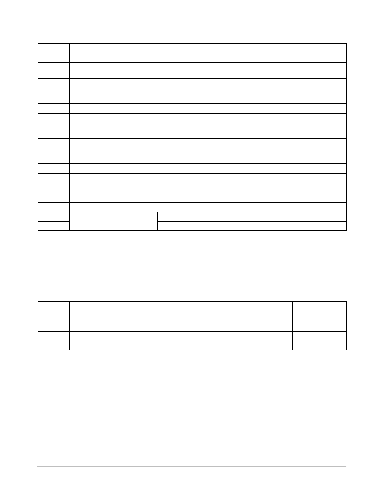
ABSOLUTE MAXIMUM RATINGS (All voltages are referenced to SGND pin unless otherwise noted)
Symbol
V
DD
V
DDL
V
SW
V
DDH
V
BST_SGND
V
BST_SW
V
HOSRC
V
HOSNK
V
PGND
V
LOSRC
V
LOSNK
V
IN
V
DT
Low−side and logic−fixed supply voltage (PGND = SGND) −0.3 20 V
Low−side supply voltage V
connect to external voltage source, referenced to PGND)
High−side common mode voltage range (SW) −3.5 650 V
High−side floating supply voltage V
do not connect to external voltage source; referenced to SW)
High−side floating supply voltage V
High−side floating supply voltage V
,
High−side floating driver sourcing/sinking output voltage (referenced to SW) −0.3 V
PGND voltage −3.5 3.5 V
,
Low−side driver sourcing/sinking output voltage (referenced to PGND) −0.3 V
Logic input voltage (HIN, LIN, and EN) −0.3 VDD+0.3 V
Dead−time control voltage (DT) −0.3 VDD+0.3 V
dVSW/dt Allowable offset voltage slew rate − 200 V/ns
T
T
STG
Operating Junction Temperature − 150 °C
J
Storage Temperature Range −55 150 °C
Electrostatic Discharge Capability
Stresses exceeding those listed in the Maximum Ratings table may damage the device. If any of these limits are exceeded, device functionality
should not be assumed, damage may occur and reliability may be affected.
1. Refer to ELECTRICAL CHARACTERISTICS, RECOMMENDED OPERATING RANGES and/or APPLICATION INFORMATION for Safe
Operating parameters.
– PGND voltage must not exceed 20 V
2. V
DD
3. This device series incorporates ESD protection and is tested by the following methods:
ESD Human Body Model tested per ANSI/ESDA/JEDEC JS−001−2012
ESD Charged Device Model tested per JESD22−C101.
4. This device contains latch−up protection and exceeds 100 mA per JEDEC Standard JESD78 Class I.
Rating Min Max Unit
(internally regulated; output only, do not
DDL
(internally regulated; output only,
DDH
BST
(referenced to SW) −0.3 20 V
BST
−0.3 5.5 V
−0.3 5.5 V
−0.3 670 V
DDH
DDL
Human Body Model (Note 3) − 1 kV
Charged Device Model (Note 3) − 1 kV
+0.3 V
+0.3 V
THERMAL CHARACTERISTICS
Symbol Rating Value Unit
q
JA
P
Thermal Characteristics,
QFN15 4x4 (Note 5)
Thermal Resistance Junction−Ambient (Note 6)
Power Dissipation (Note 6)
D
QFN15 4x4 (Note 5)
IS0P 245
IS2P 188
IS0P 0.51
IS2P 0.665
°C/W
W
5. Refer to ELECTRICAL CHARACTERISTICS, RECOMMENDED OPERATING RANGES and/or APPLICATION INFORMATION for Safe
Operating parameters.
6. JEDEC standard: JESD51−2, JESD51−3. Mounted on 76.2×114.3×1.6 mm PCB (FR−4 glass epoxy material).
IS0P: one single layer with zero power planes
IS2P: one single layer with two power planes
www.onsemi.com
4
NCP51820
RECOMMENDED OPERATING CONDITIONS (All voltages are referenced to SGND pin unless otherwise noted)
Symbol
V
DD
Low−side and logic−fixed supply voltage 9 17 V
VSW−SGND SW−SGND maximum dc offset voltage (High−Side driver) − 580 V
V
HOSRC
V
LOSRC
V
BST
, V
HOSNK
, V
LOSNK
V
IN
High−side floating supply voltage V
High−side floating driver sourcing/sinking output voltage − V
Low−side driver sourcing/sinking output voltage − V
Logic input voltage (HIN, LIN, and EN) − 17 V
PGND−SGND PGND−SGND maximum dc offset voltage (Low−Side driver) −3.0 3.0 V
Functional operation above the stresses listed in the Recommended Operating Ranges is not implied. Extended exposure to stresses beyond
the Recommended Operating Ranges limits may affect device reliability.
Rating Min Max Unit
BST
− VSW+17 V
DDH
DDL
V
V
ELECTRICAL CHARACTERISTICS (V
T
= 25°C, for min/max values T
A
The V
and IO parameters are referenced to VSW and PGND and are applicable to the respective outputs HOSRC, HOSNK, LOSRC,
O
= −40°C to +125°C, unless otherwise specified.) The V
A
BIAS
(VDD, V
) = 15 V, DT = SGND = PGND and C
BST
and IIN parameters are referenced to SGND.
IN
= 330 pF for typical values
LOAD
and LOSNK.
Symbol
Parameter Test Conditions and Description Min Typ Max Unit
POWER SUPPLY SECTION (VDD)
I
QDD
I
PDD
V
DDUV+
V
DDUV−
V
DDHYS
t
UVDDFLT
Quiescent VDD supply current V
Operating VDD supply current f
VDD UVLO positive going threshold V
VDD UVLO negative going threshold V
VDD UVLO Hysteresis V
VDD UVLO Filter Delay Time (Note 7) − 5.3 −
= V
LIN
LIN
DD
DD
DD
= 0 V, EN = 0 V − 100 150
HIN
= 500 kHz, average value − 1.5 2.5 mA
= Sweep 8.0 8.5 9.0 V
= Sweep 7.5 8.0 8.5 V
= Sweep − 0.5 − V
BOOTSTRAPPED POWER SUPPLY SECTION
I
LK
I
QBST
I
PBST
V
BSTUV+
V
BSTUV−
V
HYST
Offset supply leakage current V
Quiescent V
Operating V
V
UVLO positive going threshold V
BST
V
UVLO negative going threshold V
BST
V
UVLO Hysteresis V
BST
supply current V
BST
supply current f
BST
BST
LIN
HIN
DD
DD
DD
= V
= 600 V − − 10
SW
= V
= 0 V, EN = 5 V − 35 100
HIN
= 500 kHz, average value − 1.5 2.5 mA
= 12 V − 6.5 − V
= 12 V − 6.0 − V
= 12 V − 0.5 − V
GATE DRIVER POWER SUPPLY SECTION
V
V
DDH
DDL
V
DDH−VSW
V
DDL
regulated voltage
−PGND regulated voltage 4.94 5.20 5.46 V
0 mA < IO < 10 mA
4.94 5.20 5.46 V
INPUT LOGIC SECTION (HIN, LIN and EN)
V
V
V
IN_HYS
I
IN+
I
IN−
R
INH
INL
IN
High Level Input Voltage Threshold − − 2.5 V
Low Level Input Voltage Threshold 1.2 − − V
Input Logic Voltage Hysteresis − 0.5 − V
High Level Logic Input Bias Current V
Low Level Logic Input Bias Current V
Input Pull−down Resistance V
HIN
HIN
HIN
= V
= 5 V 9 15 21
LIN
= V
= 0 V − − 2.2
LIN
= V
= 5 V − 333 −
LIN
DEAD−TIME SECTION
V
DT,MIN
t
DT,MIN
Minimum Dead−Time Control Voltage
R
= 30 kW 0.45 0.60 0.75 V
DT
22 30 38 ns
mA
ms
mA
mA
mA
mA
kW
www.onsemi.com
5
NCP51820
ELECTRICAL CHARACTERISTICS (V
T
= 25°C, for min/max values T
A
The V
and IO parameters are referenced to VSW and PGND and are applicable to the respective outputs HOSRC, HOSNK, LOSRC,
O
= −40°C to +125°C, unless otherwise specified.) The V
A
BIAS
(VDD, V
) = 15 V, DT = SGND = PGND and C
BST
and IIN parameters are referenced to SGND.
IN
= 330 pF for typical values
LOAD
and LOSNK. (continued)
Symbol UnitMaxTypMinTest Conditions and DescriptionParameter
DEAD−TIME SECTION
V
DT,MAX
t
DT,MAX
Dt
V
DT,0
V
DT,OLE
DT
Maximum Dead−Time Control Voltage
Dead−Time mismatch between
LO → HO and HO → LO
Dead−Time Disable Threshold Cross conduction prevention active 0.35 0.40 0.45 V
High− & Low−Side Overlap Enable
Threshold
R
= 200 kW 3.1 4.0 4.8 V
DT
160 200 240 ns
R
= 30 kW
DT
R
= 200 kW
DT
Cross conduction prevention
− − 5 ns
− − 10 ns
5.5 6.0 6.5 V
disabled
PROTECTION SECTION
V
UVTH_VDDX+
V
UVTH_VDDX−
UVLO Threshold on VDDH and VDDL
positive going threshold
UVLO Threshold on VDDH and VDDL
negative going threshold
4.15 4.40 4.70 V
4.0 4.2 4.5 V
TSD Thermal Shutdown (Note 7) 150 − − °C
hys Hysteresis of Thermal Shutdown
− 50 − °C
(Note 7)
GATE DRIVE OUTPUT SECTION
V
OH
V
OL
I
OSRC
I
OSNK
High−level output voltage,
V
VDDH−VHOSRC
or V
VDDL−VLOSRC
Low−level output voltage,
V
HOSNK−VSW
or V
LOSNK
–PGND
Peak source current (Note 7)
Peak sink current (Note 7)
I
= 10 mA − 10 40 mV
OSRC
I
= 10 mA − 5 20 mV
OSNK
C
LOAD
C
LOAD
= 200 pF, R
= 200 pF, R
gate
gate
= 1 W
= 1 W
0.9 1.0 − A
1.8 2.0 − A
Product parametric performance is indicated in the Electrical Characteristics for the listed test conditions, unless otherwise noted. Product
performance may not be indicated by the Electrical Characteristics if operated under different conditions.
7. Guaranteed by design, is not tested in production.
DYNAMIC ELECTRICAL CHARACTERISTICS (V
values T
Symbol
t
=25°C, for min/max values TA=−40°C to +125°C, unless otherwise specified.) (Notes 9)
A
Parameter Test Conditions Min Typ Max Unit
I
QDD
t
PDLON
t
PDLOFF
t
PDHON
PDHOFF
t
RL
t
FL
t
RH
t
FH
Quiescent VDD supply current V
LOSRC turn−on propagation delay
LIN rising to LOSRC rising (50% to 10%) − 25 50 ns
time
LOSNK turn−off propagation delay
LIN falling to LOSNK falling (50% to 90%) − 25 50 ns
time
HOSRC turn−on propagation delay
time
HOSNK turn−off propagation delay
time
HIN rising to HOSRC rising (50% to 10%)
SW = PGND
HIN falling to HOSNK falling (50% to 90%)
SW = PGND
LOSRC turn−on rising time − 2 4 ns
LOSNK turn−off falling time − 1.5 3.0 ns
HOSRC turn−on rising time
SW = PGND
HOSNK turn−off falling time − 1.5 3.0 ns
(VDD, V
LIN
BIAS
= V
BST
= 0 V, EN = 0 V − 100 150
HIN
www.onsemi.com
6
)=15 V, DT=SGND=PGND and C
− 25 50 ns
− 25 50 ns
− 2 4 ns
=330 pF, for typical
LOAD
mA
NCP51820
DYNAMIC ELECTRICAL CHARACTERISTICS (V
values T
=25°C, for min/max values TA=−40°C to +125°C, unless otherwise specified.) (Notes 9) (continued)
A
BIAS
(VDD, V
)=15 V, DT=SGND=PGND and C
BST
=330 pF, for typical
LOAD
Symbol UnitMaxTypMinTest ConditionsParameter
Dt
DEL
t
PW
Propagation Delay match HIN to HO and LIN to LO, SW = PGND − − 5 ns
Minimum input pulse width − − 10 ns
Product parametric performance is indicated in the Electrical Characteristics for the listed test conditions, unless otherwise noted. Product
performance may not be indicated by the Electrical Characteristics if operated under different conditions.
8. This parameter, although guaranteed by design, is not tested in production.
9. Performance guaranteed over the indicated operating temperature range by design and/or characterization tested at T
= TA = 25°C.
J
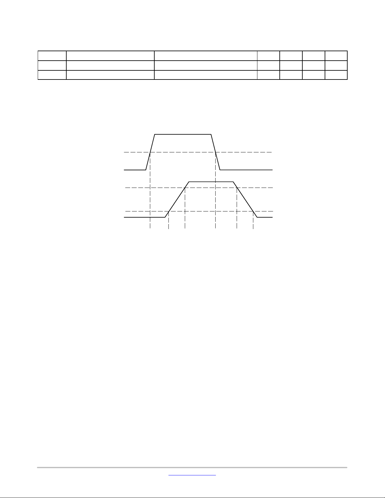
Timing Diagram
Shown in Figure 4 are the timing waveform definitions matching the specified dynamic electrical characteristics specified
in the gate drive output section.
50%
HIN
(LIN)
90%
10%
HO
(LO)
t
PDHON
(t
PDLON
Figure 4. Input to Output Timing Diagram
)
t
RH
(tRL)
t
PDHOFF
(t
PDLOFF
t
FH
)
(tFL)
www.onsemi.com
7

NCP51820
0
14
12
10
8
[mA]
6
PDD
I
4
2
0
10 100 10000
Figure 5. Operating VDD Supply Current (I
CLOAD = 0 pF
CLOAD = 100 pF
F
= F
HIN
LIN
1000
[kHz]
PDD
Frequency (VDD = 12 V, SW = PGND, EN = VDD,
Both Outputs Switching)
140
125
110
[mA]
95
80
QBST
, I
65
QDD
I
50
35
20
−40 −200 20406080100120
Temperature [°C]
Figure 7. Quiescent Current (I
IQDD, EN = 0 V
IQBST, EN = 5 V
, I
QBST
) vs.
QDD
Temperature
) vs.
60
50
40
30
[mA]
PDD
I
20
10
0
10 100 1000
Figure 6. Operating VDD Supply Current (I
CLOAD = 330 pF
CLOAD = 1 nF
F
= F
HIN
LIN
1000
[kHz]
PDD
Frequency (VDD = 12 V, SW = PGND, EN = VDD,
Both Outputs Switching)
4.0
3.0
3.0
2.5
2.0
1.5
IDD, IBST [mA]
1.0
0.5
0.0
−40 −20 0 20 40 60 80 100 120
Figure 8. Operating Current (I
LIN = 100 kHz HIN = 100 kHz
LIN = 500 kHz HIN = 500 kHz
LIN = 1 MHz HIN = 1 MHz
Temperature [°C]
, I
PDD
PBST
) vs.
Temperature
) vs.
www.onsemi.com
8

NCP51820
10.0
9.5
9.0
[V]
8.5
8.0
DDUVLO
7.5
V
7.0
6.5
6.0
−40
−20 0 20 40 60 80 100 120
Figure 9. VDD UVLO (V
Temperature [°C]
DDUVLO+
, V
DDUVLO−
VDDUV+
VDDUV−
) vs.
Temperature
5.22
5.21
5.20
5.19
[V]
5.18
DDL
V
5.17
5.16
5.15
5.14
−40 −200 20406080100120
Temperature [°C]
Figure 11. VDDL (V
) Regulated Output Voltage
DDL
VDDH, 0 mA
VDDH, 10 mA
vs. Temperature
5.22
5.21
5.20
5.19
[V]
5.18
DDH
V
5.17
5.16
5.15
5.14
−40 −20 0 20 40 60 80 100 120
Temperature [°C]
Figure 10. VDDH (V
) Regulated Output Voltage
DDH
VDDH, 0 mA
VDDH, 10 mA
vs. Temperature
2.2
2.1
2.0
1.9
1.8
1.7
1.6
1.5
1.4
Input Logic Threshold [V]
1.3
1.2
−40 −20 0 20 40 60 80 100 120
Temperature [°C]
VINH
VINL
Figure 12. Input Logic (HIN, LIN, EN) Threshold vs.
Temperature
400
375
350
325
300
275
250
−40 −20 0 20 40 60 80 100 120
Input Logic Pull−down Resistance [kW]
Temperature [°C]
Figure 13. Input Logic (HIN, LIN, EN) Pull−down
Resistance vs. Temperature
22
20
18
16
14
12
LO Propagation Delay [ns]
10
−40 −20 0 20 40 60 80 100 120
www.onsemi.com
9
tPDLON
tPDLOFF
Temperature [°C]
Figure 14. LIN to LOSRC Propagation Delay vs.
Temperature

NCP51820
22
20
18
16
14
12
HO Propagation Delay [ns]
10
−40 −20 0 20 40 60 80 100 120
Temperature [°C]
tPDHON
tPDHOFF
Figure 15. HIN to HOSRC Propagation Delay vs.
Temperature
3.0
2.5
2.0
1.5
HO Rise and Fall Time [ns]
1.0
−40 −20 0 20 40 60 80 100 120
Temperature [°C]
tRH
tFH
3.0
2.5
2.0
1.5
LO Rise and Fall Time [ns]
1.0
−40 −20 0 20 40 60 80 100 120
Temperature [°C]
tRL
tFL
Figure 16. LOSRC Rise Time and LOSNK Fall Time vs.
Temperature
4.5
4.4
[V]
UVLO
4.3
4.2
VDDDL
4.1
4.0
−40 −20 0 20 40 60 80 100 120
Temperature [°C]
VUVTH_VDDL+
VUVTH_VDDL−
Figure 17. HOSRC Rise Time and HOSNK Fall Time
vs. Temperature
4.5
4.4
[V]
4.3
UVLO
4.2
VDDDH
4.1
4.0
−40 −20
0
20 40 60 80 100 120
Temperature [°C]
VUVTH_VDDH+
VUVTH_VDDH−
Figure 19. VDDH UVLO vs. Temperature
Figure 18. VDDL UVLO vs. Temperature
6.0
5.5
5.0
4.5
4.0
ILK [mA]
3.5
3.0
2.5
2.0
−40 −20 0 20 40 60 80 100 120
Temperature [°C]
Figure 20. VBST Leakage Current (ILK) vs.
Temperature
www.onsemi.com
10

NCP51820
0
1.2
1.0
0.8
0.6
DtDEL [ns]
0.4
0.2
0.0
−40 −200 20406080100120
Temperature [°C]
tDEL_SRC
tDEL_SNK
Figure 21. Propagation Delay Matching (HIN to HO,
LIN to LO) vs. Temperature
35
34
33
32
31
30
29
28
27
Minimum Dead−time [ns]
26
25
−40
−20 0 20 40 60 80 100 120
Temperature [°C]
2.5
2.0
1.5
1.0
0.5
0.0
−0.5
DtDT [ns]
−1.0
−1.5
−2.0
−2.5
−40 −200 2040608010012
Delta, tDT (RDT = 30 kW)
Delta, tDT (RDT = 200 kW)
Temperature [°C]
Figure 22. Dead−time Mismatch vs. Temperature
0.70
tDT, MIN; HO−LO
tDT, MIN; LO−HO
VDT, MIN
0.69
0.68
0.67
0.66
0.65
0.64
0.63
0.62
0.61
0.60
Minimum Dead−time Control Voltage [V]
Figure 23. Minimum Dead−time (RDT = 30 kW) vs. Temperature
216
214
212
210
208
206
204
Maximum Dead−time [ns]
202
200
−40 −20 0 20 40 60 80 100 120
Temperature [°C]
tDT, MIN; HO−LO
tDT, MIN; LO−HO
VDT, MIN
4.4
4.3
4.2
4.1
4.0
3.9
3.8
3.7
3.6
Figure 24. Maximum Dead−time (RDT = 200 kW) vs. Temperature
Maximum Dead−time Control Voltage [V]
www.onsemi.com
11

NCP51820
APPLICATIONS INFORMATION
The NCP51820 can be quickly configured by following the steps outlined in this section. The component references made
throughout this section refer to the schematic diagram and reference designations shown in Figure 25.
C
POWER
STAGE
VBST
VBST
C
VDDH
VDDH
R
Q
H
HOSRC
R
HOSNK
HOSRC
HOSNK
SW
15
1
2
3
4
D
BST
NCP51820
(Top View)
5
R
HBST
R
VDD
6
7
EN
14
EN
13
HIN
12
LIN
11
SGND
10
C
DTBYP
DT
9
R
8
DT
C
ENBYP
VDDVIN
C
VDD
PWM
mC
or
DSP
R
Q
L
LOSRC
R
LOSNK
Figure 25. Application Schematic, Half−Bridge Example (Kelvin Gate Return Connections Shown)
DETAILED PIN FUNCTIONALITY
Bias Supply Voltage (VDD)
A dc voltage applied to VDD provides bias for the digital
inputs, internal logic functions, high−side floating bootstrap
(VBST) bias supplying the internal high−side regulator
(VDDH) as well as providing bias directly to the internal
low−side regulator (VDDL). Because the GaN FETs receive
source current locally through the dedicated internal
regulators, a single VDD bypass capacitor, C
VDD
, is all
that’s required, connected directly between the VDD and
SGND pins. The C
capacitor should be a ceramic bypass
VDD
capacitor > 100 nF, located as close as possible to the VDD
and SGND pins to properly filter out all glitches while
switching. Under voltage lockout (UVLO) is important for
protecting the GaN FETs and power stage. The NCP51820
includes UVLO thresholds of V
V
< 8 V, OFF, making it well suited for +12 V bias
DDUV−
DDUV+
> 8.5 V, ON and
rails.
High−Side Bootstrap Voltage (VBST)
Three components make up the high side bootstrap
voltage bias serving as the input to the VDDH regulator. The
bootstrap current limiting resistor and diode, R
D
, series connected between the VDD and VBST pins
BST
and the bootstrap capacitor, C
, connected directly
VBST
BST
and
Switch node between VBST and (SW) pins. The VBST
voltage is input to an internal LDO which produces the
VDDH voltage. A large value for C
means the
VBST
C
VDDL
VDDL
LOSRC
LOSNK
PGND
bootstrap capacitor will take longer to fully charge as also
determined by the on−time of the low−side GaN. Neglecting
the effects of parasitic inductance, the minimum value
bootstrap capacitor can be approximated as:
Q
C
BST
G
+
DV
BST
Where:
Q
= total gate charge required by GaN
G
DV
= VDD − V
BST
PP
− NxV
> 6 V
F
N = number of series diodes connected
= allowable V
V
PP
droop voltage
BST
(typically less than 10% of VDD)
V
= D
F
forward voltage drop
BST
Choose a low ESR and ESL ceramic capacitor with a
voltage rating of twice the applied voltage (2 x DV
Once the bootstrap capacitor is selected, the peak charging
current can be determined by knowing the frequency and
duty cycle of the low−side gate drive.
DV
IPK+ C
BST
dV
+ C
dt
BST
BST
F
SW
D
MAX
Where:
D
F
= Max duty cycle of low−side gate drive
MAX
= Switching frequency
SW
(eq. 1)
BST
(eq. 2)
).
www.onsemi.com
12

NCP51820
The bootstrap diode, D
, needs to have a voltage rating
BST
greater than VIN, should be high−speed (low reverse
recovery), should be low current and should have very low
junction capacitance. Diode junction capacitance, C
, can
J
become more problematic due to the high dV/dt that can
appear across the GaN V
. Symptoms of high dV/dt
DS
switching can be mitigated by using a Kelvin source return
to SW, as shown in Figure 25. Another method to reduce C
is to use 2 or more diodes in series such that the sum of the
total voltage ratings from each diode is greater than VIN.
Each of the individual C
’s add reciprocally to reduce the
J
total junction capacitance. The additional number of diode
forward voltage drops must also be accounted for when
calculating C
The purpose of the bootstrap resistor, R
peak C
BST
.
BST
, is to limit
BST
charging current, IPK, especially during startup.
A small resistor may not limit the peak current enough,
resulting in excessive ringing which can cause jitter in the
high−side gate drive and/or EMI problems. A large resistor
will dissipate more power and create a longer RC time
constant causing a longer start−up time. A bootstrap resistor
in the range of 1 W < R
High−Side Linear Regulator (VDDH)
< 10 W is usually sufficient.
BST
The NCP51820 includes an internal linear regulator
dedicated to providing a tightly regulated, 5.2 V gate drive
amplitude signal to the high−side GaN FET. The VDDH
regulator appears after the bootstrap, providing the most
direct interface to the high−side GaN FET. This assures the
lowest possible parasitic capacitance, required for meeting
high−speed switching requirements of GaN. The VDDH
regulator is referenced between VDDH and the SW pins and
can float between a common mode voltage range of −3.5 V
up to 650 V. Source current for the high−side GaN FET is
provided from the charge stored in C
between VDDH and SW. The value of the C
VDDH
VDDH
connected
capacitor
is a function of the gate charge requirement of the GaN FET.
The VDDH regulator also includes dedicated UVLO
thresholds of V
V
UVTH_VDDH−
Switch Node (SW)
< 4.3 V, OFF.
UVTH_VDDH+
> 4.5 V, ON and
The SW pin serves as the high−side, gate drive, return
reference. As shown in Figure 2, the high−side level shifter,
drive logic, PMOS sink and VDDH regulator are referenced
to SW. For GaN FETs that include a source Kelvin return, a
direct connection should be made from SW to the GaN FET
Kelvin return. C
VDDH
and C
should then be referenced
BST
to the SW pin but separate from the power stage switch node
as shown in Figure 25. For GaN FETs that do not include a
dedicated source Kelvin pin, best practice PCB layout
techniques should be used to isolate the gate drive return
current from the power stage, switch node current. Please
refer to document AND9932
, for NCP51820 and
high−speed GaN, PCB layout tips.
Low−Side Linear Regulator (VDDL)
The NCP51820 includes an internal linear regulator
dedicated to providing a tightly regulated, 5.2 V gate drive
amplitude signal to the low−side GaN FET. The VDDL
regulator is fed directly from VDD, providing the most
direct interface to the low−side GaN FET. This assures the
lowest possible parasitic capacitance, required for meeting
high−speed switching requirements of GaN. The VDDL
J
regulator is referenced between VDDL and the power
ground (PGND) pins and is capable of operating from
common mode voltage range between −3.5 V to +3.5 V.
Source current for the low−side GaN FET is provided from
the charge stored in the C
and PGND. The value of the C
connected between VDDL
VDDL
capacitor is a function
VDDL
of the gate charge requirement of the low−side GaN FET.
The VDDL regulator also includes dedicated UVLO
thresholds of V
V
UVTH_VDDL−
Signal Ground (SGND) and Power Ground (PGND)
UVTH_VDDL+
< 4.3 V, OFF.
> 4.5 V, ON and
SGND is the GND for all internal control logic and digital
inputs. Internally, the SGND and PGND pins are isolated
from each other.
PGND serves as the low−side, gate drive, return
reference. As shown in Figure 2, the low−side level shifter,
drive logic, PMOS sink and VDDL regulator are referenced
to PGND. For GaN FETs that include a source Kelvin return,
a direct connection should be made from PGND to the GaN
FET Kelvin return. C
should then be referenced to the
VDDL
PGND but separate from the power stage ground as shown
in Figure 25. For GaN FETs that do not include a dedicated
source Kelvin pin, best practice PCB layout techniques
should be used to isolate the gate drive return current from
the power stage, ground return current. Please refer to
document AND9932
, for NCP51820 and high−speed GaN,
PCB layout tips.
For half−bridge power topologies or any applications
using a current sense transformer, SGND and PGND must
be connected together on the PCB. In such applications, it is
recommended to connect the SGND and PGND pins
together with a short, low−impedance trace on the PCB as
close to the NCP51820 as possible. Directly beneath the
NCP51820 is an ideal way to make the SGND to PGND
connection.
For low−power applications, such as the active−clamp
flyback or forward shown in Figure 26, a current sensing
resistor, R
, located in the low−side GaN FET source leg
CS
is commonly used. In such applications, the NCP51820
PGND and SGND pins must not be connected on the PCB
because R
would essentially be shorted through this
CS
connection. The NCP51820 low−side drive circuit is able to
withstand −3.5 V to +3.5 V of common mode voltage. Since
most current sense voltage signals are less than 1 V, the
low−side drive stage can easily “float” above the voltage,
www.onsemi.com
13

NCP51820
V
, generated by the current sense. For the active clamp
RCS
example in Figure 26, the entire low−side gate drive, shown
in the shaded box, is floating above V
because it ensures no loss of gate drive amplitude so the full
5.2 V, VDDL voltage appears at the low−side GaN FET
POWER
STAGE
Q
H
. This is important
RCS
C
CL
R
HOSRC
R
HOSNK
C
VDDH
C
VBST
VDDH
HOSRC
HOSNK
SW
gate−source terminals. A low impedance current sense
resistor is recommended. Please refer to document
AND9932, for NCP51820 and high−speed GaN, PCB
layout tips.
R
D
HBST
BST
R
VBST
15
1
2
3
4
NCP51820
(Top View)
5
VDD
6
7
EN
14
EN
13
HIN
12
LIN
11
SGND
10
C
DTBYP
DT
9
R
8
DT
C
ENBYP
VDDVIN
C
VDD
PWM
mC
or
DSP
R
Q
L
V
RCS
LOSRC
R
LOSNK
R
CS
Figure 26. Application Schematic, Active Clamp, Low−Side, Floating Gate Drive Example
Input (HIN, LIN)
Both independent PWM inputs are Schmitt trigger,
Transistor−Transistor Logic (TTL) compatible and are
internally pulled low to SGND such that each corresponding
driver input is defaulted to the inactive (disabled) state. The
TTL input thresholds provide buffer and logic level
translation functions capable of operating from a variety of
PWM signals up to VDD of the NCP51820. TTL levels
permit the inputs to be driven from a range of input logic
signal levels for which a voltage greater than 2.5 V
maximum is considered logic high. Both input thresholds
meet industry−standard, TTL−logic defined thresholds and
are therefore independent of V
voltage. A typical
DD
hysteresis voltage of 0.5 V is specified for each driver input.
For optimal high−speed switching performance, the driving
signal for the TTL inputs should have fast rising and falling
edges with a slew rate of 6 V/ms or faster, so a rise time from
0 to 3.3 V should be 550 ns or less.
C
VDDL
VDDL
LOSRC
LOSNK
PGND
Enable (EN)
Enable (EN) is internally pulled low to SGND so the
driver is always defaulted to a disabled output status. Similar
to HIN and LIN, EN is a Schmitt trigger TTL compatible
input. Pulling the EN pin above 2.5 V maximum, enables the
outputs, placing the NCP51820 into an active ready state.
Due to the nature of high−speed switching associated with
GaN power stages, and for improved noise immunity, it is
recommended to connect the EN pin to VDD through a 1 kW
(or less) pull−up resistor. For applications where the EN pin
is actively controlled, the EN pin can be driven direct but
should be bypassed with a 10 nF decoupling capacitor. As
shown in Figure 27, if EN is pulled low during normal
operation, the driver outputs are immediately disabled, even
terminating an active HIN or LIN pulse mid –cycle during
the on−time. When EN is toggled high, during normal
operation, a cycle−by−cycle, edge−triggered logic function
is employed to prevent shortened, erroneous control pulses
from being processed by the output. This behavior is
highlighted in Figure 27, where EN transitions high at the
same time the HIN (or LIN) input pulse is high. In this way,
the NCP51820 is intelligent by waiting until the next rising
edge to process the full input signal to the output driver
stage.
www.onsemi.com
14

HIN
(LIN)
HO
(LO)
NCP51820
EN
Figure 27. Timing Chart of Enable Function
Dead−Time Control (DT)
Accurately ensuring some minimal amount of dead−time
between the high−side and low−side gate drive output
signals is critical for safe, reliable optimized operation of
any high−speed, half−bridge power stage. The DT should be
bypassed with a 100 nF (C
) ceramic capacitor placed
DTBYP
closest to the pin and directly between DT and SGND. If
used, the R
parallel with C
resistor should then be placed directly in
DT
The NCP51820 offers four unique
DTBYP.
mode settings to utilize dead−time in such a way to be fully
compatible with any control algorithm.
MODE A:
Connect DT to SGND; When the DT pin voltage, V
less than 0.5 V typical (R
= 0 W), the DT programmability
DT
DT
, is
is disabled and fixed dead−time, anti−cross−conduction
protection is enabled. If HIN and LIN are overlapping by X
ns, then X ns of dead−time is automatically inserted.
Conversely, if HIN and LIN have greater than 0 ns of
dead−time, then the dead−time is not modified by the
NCP51820 and is passed through to the output stage as
defined by the controller. This type of dead−time control is
preferred when the controller will be making the necessary
dead−time adjustments but needs to rely on the NCP51820
dead−time control function for anti−cross−conduction
protection.
HIN
50% 50%
LIN
50% 50%
LO
HO
Figure 28. Internal Dead−Time Definitions
DT
50%
DT
50%
External Shutdown
MODE B:
Connect a 25 kW < R
< 200 kW Resistor from DT to
DT
SGND; Dead−time is programmable by a single resistor
connected between the DT and SGND pins. The amount of
desired dead−time can be programmed via the dead−time
resistor, R
, between the range of 25 kW < R
DT
to obtain an equivalent dead−time, proportional to R
the range of 25 ns < t
< 200 ns. If either edge between HIN
DT
and LIN result in a dead−time less than the amount set by
R
, the set DT value shall be dominant. If either edge
DT
between HIN and LIN result in a dead−time greater than the
amount set by R
dominant. The control voltage range, V
< V
< 4 V. DT programmability is summarized and shown
DT
, the controller dead−time shall be
DT
, for RDT is 0.5 V
DT
graphically in Figure 29.
MODE C:
Connect a 249 kW Resistor from DT to SGND; Connect a
249 kW resistor between DT and SGND to program the
maximum dead−time value of 200 ns. The control voltage
range, V
, for assuring t
DT
= 200 ns is 4 V < V
DT
programmability is summarized and shown graphically in
Figure 29.
MODE D:
Connect DT to VDD; When the DT pin voltage, V
greater than 6 V (pulled up to VDD through 10 kW resistor),
anti−cross−conduction protection is disabled, allowing the
output signals to overlap. This operating mode is suitable for
applications where it is desired to have both driver output
stages switching simultaneously. If choosing this operating
mode while driving a half−bridge power stage, extreme
caution should be taken, as cross conduction can potentially
damage power components if not accounted for. This type
of dead−time control is preferred when the controller will be
making extremely accurate dead−time adjustments and can
respond to the potential of over−current faults on a
cycle−by−cycle basis. DT programmability is summarized
and shown graphically in Figure 29.
< 200 kW
DT
< 5 V. DT
DT
DT
DT
, in
, is
www.onsemi.com
15

NCP51820
VDT [V]
No dead−time
Mode A: V
6
t
= SGND = 0 V
DT
Cross−conduction prevention active
5
4
3
2
1
0
25 50 100 150 200 250 300
< 0.5 V
DT
Dead−time Control Range
Mode B: 0.5 V < V
= R
x 1 ns/kW
DT
t
DT
Cross−conduction prevention active
DT
< 4 V
Maximum dead−time
MODE C: 4 V<VDT<5 V
t
=200 ns
DT
Cross−conduction prevention on
RDT [kW]
Figure 29. Dead−Time Control, tDT, VDT vs R
Output ENABLED
MODE D: 6 V < V
t
= 0 ns
DT
Cross−conduction prevention disabled
< VDD (pull−up)
DT
DT
t [ns]
DT
200
150
100
50
0
High−Side Output (HOSRC and HOSNK)
The NCP51820 high−side drive stage is level shifted from
HIN and SGND and referenced to SW and can withstand a
common mode voltage range from −3.5 V to +650 V.
HOSRC and HOSNK outputs are driven by a pure MOS,
low−impedance totem pole output stage to ensure tightly
regulated, low stray capacitance, full VDDH switching. The
output slew rate is determined primarily by VDDH and the
Q
of the high−side GaN FET. The turn−on (HOSRC) and
G
turn−off (HOSNK) functions each have dedicated pins. This
allows a single resistor between each pin and the high−side
GaN FET gate to independently control gate ringing as well
as fine tuning dV
/dt turn−on and turn−off transitions
DS
present on the GaN drain−source voltage. The driver
provides the high peak currents necessary for high−speed
switching, even at the Miller plateau voltage. The outputs of
the NCP51820 are rated to 1 A peak current source
(HOSRC) and 2 A sink (HOSNK).
Low−Side Output (LOSRC and LOSNK)
The NCP51820 low−side drive stage is level shifted from
LIN and SGND and referenced to PGND and can withstand
a common mode voltage range from −3.5 V to +3.5 V.
LOSRC and LOSNK outputs are driven by a pure MOS,
low−impedance totem pole output stage to ensure tightly
regulated, low stray capacitance, full VDDL switching. The
output slew rate is determined primarily by VDDL and the
Q
of the low−side GaN FET. The turn−on (LOSRC) and
G
turn−off (LOSNK) functions each have dedicated pins. This
allows a single resistor between each pin and the low−side
GaN FET gate to independently control gate ringing as well
as fine tuning dV
/dt turn−on and turn−off transitions
DS
present on the GaN drain−source voltage. The driver
provides the high peak currents necessary for high−speed
switching, even at the Miller plateau voltage. The outputs of
the NCP51820 are rated to 1 A peak current source
(LOSRC) and 2 A sink (LOSNK). The high−side and
low−side drive stage can be thought of as two independent
floating driver channels. Both driver output channels are
perfectly suited for driving the latest generation HEMT GIT
GaN FETs which require constant current into the internal
gate clamp or HEMT GaN FETs which are strictly
unclamped, voltage controlled devices requiring tightly
regulated gate drive signals.
Input to Output Protection Functions
Figure 30 graphically summarizes the input to output
protection functions for the following three cases:
Case A:
External shutdown due to EN pulled low. Outputs are
immediately terminated when EN is pulled low. The second
rising edge of either HIN or LIN is processed to the output
when EN is pulled high.
www.onsemi.com
16

NCP51820
Case B:
UVLO protection event during shutdown and start−up.
Crossing the UVLO ON and OFF thresholds has the same
effect as EN, where outputs are immediately terminated
when UVLO OFF is reached. The second rising edge of
either HIN or LIN is processed to the output when UVLO
ON is reached.
HIN
LIN
EN
V
DD
HO
A
Shutdown
V
Cycle−by−Cycle
Shutdown
Disregard Disregard
DDUVL
B
UVLO
Case C:
Anti−cross−conduction, shoot−through protection. As
described in the DT section MODE A
, when the DT pin is
connected SGND, any amount of HIN to LIN overlap is
translated to HO to LO dead−time.
C
Cycle−by−Cycle
Shutdown
Shoot−Through
Prevention
LO
Figure 30. Protection Functions, Timing Diagram
PCB LAYOUT
When beginning a PCB design using GaN FETs, the best
layout procedure is one that is priority−driven as listed
below. Each of these “summary” comments are highlighted
in more detail with clarifying diagrams in document
AND9932
, NCP51820 and high−speed GaN, PCB layout
tips.
1. Multi−layer PCB designs with proper use of
ground/return planes as described in this document
are a must. High frequency, high voltage, high dV/dt
and high di/dt all warrant the need for a multi−layer,
PCB design approach. Inexpensive, single−layer,
PCB designs do not allow for proper routing or
design of ground planes necessary to realize the full
benefits of a GaN based power stage.
2. Begin by placing the most noise sensitive
components near the NCP51820 first. VDD, VDDH,
VDDL, EN and DT bypass capacitors as well as the
VBST capacitor, resistor and diode should be placed
as close to their respective pins as possible.
3. Place the DT resistor directly next to C
DTBYP
and the
DT and SGND pins.
4. Place the HO and LO, source and sink gate drive
resistors as close to the GaN FETs as possible.
DT DT
5. Move the NCP51820 and associated components
close to the GaN FET source and sink resistors.
6. If possible, arrange the GaN FETs in a “staggered”
pattern with the goal of maintaining the HO and LO
gate drive lengths as closely matched as possible. To
avoid high current and high dV/dt through vias, it is
preferred that both GaN FETs be located on the same
side of the PCB as the NCP51820.
7. The HO and LO gate drives should be considered as
two independent gate drive circuits that are
electrically isolated from each other. HO and LO will
therefore each require dedicated copper land return
planes on layer 2 directly beneath layer 1 gate drive
routing.
Proper routing of the power loop, switch−node, gate drive
loops and use of planes are critical for a successful GaN PCB
design. For the gate drives, proper routing and noise
isolation will help reduce additional parasitic loop
inductance, noise injection, ringing, gate oscillations and
inadvertent turn−on. The goal is to design a high frequency,
power PCB that is thoughtful with regard to proper
grounding while maintaining controlled current flow
through direct pathway connections with minimal loop
distances.
www.onsemi.com
17

NCP51820
COMPONENT PLACEMENT AND ROUTING
The diagram shown in Figure 31 highlights the critical
component placement around the NCP51820 and the
interface to the HS and LS GaN FETs. The strategic
placement of critical components around the NCP51820,
use of dedicated ground and return planes, Kelvin source
connections and direct gate drive routing are discussed in
detail in document AND9932
, NCP51820 and high−speed
GaN, PCB layout tips.
HS SOURCE
AND SINK
GATE
RESISTORS
VBULK
HS GaN FET
POWER
SWITCH
NODE
POWER PGND
(ISOLATED FROM SWITCH NODE)
HS GATE RETURN PLANE
LS GaN FET
VBST CAPACITOR
SGND PLANE
VBST DIODE
VBST
RESISTOR
VDD
CAPACITORS
VDDH BYPASS
CAPACITOR
NCP51820
DT RESISTOR
VDDL BYPASS
CAPACITOR
LS SOURCE AND SINK
GATE RESISTORS
LS GATE RETURN
PLANE (ISOLATED
FROM POWER PGND)
Figure 31. NCP51820 Component Placement
Thermal Guidelines
High−speed, gate drivers used to switch GaN FETs at high
frequencies can dissipate significant amounts of power. It is
important to determine the driver power dissipation and the
resulting junction temperature in the application to ensure
the IC is operating within acceptable temperature limits.
The total power dissipation in a gate driver is the sum of
two components, P
P
+ 2 P
TOTAL
GATE
and P
GATE
DYNAMIC
) P
DYNAMIC
:
(eq. 3)
Gate Driving Loss: The most significant power loss
results from supplying gate current (charge per unit time) to
switch the GaN FETs on and off at the switching frequency.
The power dissipation that results from driving a GaN FET
with a specified gate−source voltage, V
Q
, at switching frequency, FSW, is determined by:
G
P
+ QG VGS F
GATE
SW
, with gate charge,
GS
(eq. 4)
This needs to be calculated for the high−side and low−side
GaN FETs where the Q
can possibly be different if the
G
devices are not the same
Dynamic Predrive / Shoot−through Current: Power loss
resulting from internal current consumption under dynamic
operating conditions can be obtained using the “I
PDD
vs.
Frequency” graphs in Figure 5 and Figure 6 to determine the
current, I
flowing from VDD under actual operating
PDD
conditions.
P
DYNAMIC
+ I
PDD
V
DD
(eq. 5)
Once the power dissipated in the driver is determined, the
driver junction temperature rise with respect to the PCB can
be evaluated using the thermal equation, given below:
TJ+ (P
TOTAL
qJA) ) T
B
(eq. 6)
Where:
= driver junction temperature
T
J
ĂĂĂĂĂĂĂĂĂq
= thermal characterization parameter relating
JA
temperature rise to total power dissipation
T
= board temperature in location defined
B
www.onsemi.com
18

NCP51820
As an example, consider an application driving two
GaN FETs with a gate charge of 5 nC each with V
(V
DDH
= V
= 5.2 V). At a switching frequency of
DDL
DD
= 12 V
500 kHz, the total power dissipation is:
P
+ 5nC 5.2 V 500 kHz 2 + 26 mW
GATE
P
DYNAMIC
P
TOTAL
+ 4mA 12 V + 48 mW
+ 74 mW
(eq. 7)
(eq. 8)
(eq. 9)
The QFN15 4x4 package has a junction−to−ambient
thermal characterization parameter of q
= 245°C/W. In a
JA
system application, the localized temperature around the
device is a function of the layout and construction of the
PCB along with airflow across the surfaces. To ensure
reliable operation, the maximum junction temperature of the
device must not exceed the absolute maximum rating of
150°C; with 80% derating, T
would be limited to 120°C.
J
Rearranging Equation 6 determines the board temperature
required to maintain the junction temperature below 120°C:
TB+ TJ* (P
T
≤ 120°C * (74 mW 245°CńW) + 102°C
B
TOTAL
qJA)
(eq. 10)
(eq. 11)
Similarly, eq. 6 can be used to calculate the junction
temperature (operating near room temperature) as:
TJ+ (74 mW 245°CńW) ) 25°C
TJ+ 43.13°C
(eq. 12)
(eq. 13)
www.onsemi.com
19

MECHANICAL CASE OUTLINE
PACKAGE DIMENSIONS
QFN15 4x4, 0.5P
CASE 485FN
ISSUE B
DATE 24 JUL 2019
GENERIC
MARKING DIAGRAM*
XXXXXX
XXXXXX
ALYWG
G
XXXXXX = Specific Device Code
A = Assembly Location
L = Wafer Lot
Y = Year
W = Work Week
G = Pb−Free Package
(Note: Microdot may be in either location)
DOCUMENT NUMBER:
DESCRIPTION:
ON Semiconductor and are trademarks of Semiconductor Components Industries, LLC dba ON Semiconductor or its subsidiaries in the United States and/or other countries.
ON Semiconductor reserves the right to make changes without further notice to any products herein. ON Semiconductor makes no warranty, representation or guarantee regarding
the suitability of its products for any particular purpose, nor does ON Semiconductor assume any liability arising out of the application or use of any product or circuit, and specifically
disclaims any and all liability, including without limitation special, consequential or incidental damages. ON Semiconductor does not convey any license under its patent rights nor the
rights of others.
© Semiconductor Components Industries, LLC, 2018
98AON81104G
QFN15 4x4, 0.5P
*This information is generic. Please refer to
device data sheet for actual part marking.
Pb−Free indicator, “G” or microdot “ G”,
may or may not be present. Some products
may not follow the Generic Marking.
Electronic versions are uncontrolled except when accessed directly from the Document Repository.
Printed versions are uncontrolled except when stamped “CONTROLLED COPY” in red.
PAGE 1 OF 1
www.onsemi.com

ON Semiconductor and are trademarks of Semiconductor Components Industries, LLC dba ON Semiconductor or its subsidiaries in the United States and/or other countries.
ON Semiconductor owns the rights to a number of patents, trademarks, copyrights, trade secrets, and other intellectual property. A listing of ON Semiconductor ’s product/patent
coverage may be accessed at www.onsemi.com/site/pdf/Patent−Marking.pdf
ON Semiconductor makes no warranty, representation or guarantee regarding the suitability of its products for any particular purpose, nor does ON Semiconductor assume any liability
arising out of the application or use of any product or circuit, and specifically disclaims any and all liability, including without limitation special, consequential or incidental damages.
Buyer is responsible for its products and applications using ON Semiconductor products, including compliance with all laws, regulations and safety requirements or standards,
regardless of any support or applications information provided by ON Semiconductor. “Typical” parameters which may be provided in ON Semiconductor data sheets and/or
specifications can and do vary in different applications and actual performance may vary over time. All operating parameters, including “Typicals” must be validated for each customer
application by customer’s technical experts. ON Semiconductor does not convey any license under its patent rights nor the rights of others. ON Semiconductor products are not
designed, intended, or authorized for use as a critical component in life support systems or any FDA Class 3 medical devices or medical devices with a same or similar classification
in a foreign jurisdiction or any devices intended for implantation in the human body. Should Buyer purchase or use ON Semiconductor products for any such unintended or unauthorized
application, Buyer shall indemnify and hold ON Semiconductor and its officers, employees, subsidiaries, affiliates, and distributors harmless against all claims, costs, damages, and
expenses, and reasonable attorney fees arising out of, directly or indirectly, any claim of personal injury or death associated with such unintended or unauthorized use, even if such
claim alleges that ON Semiconductor was negligent regarding the design or manufacture of the part. ON Semiconductor is an Equal Opportunity/Affirmative Action Employer. This
literature is subject to all applicable copyright laws and is not for resale in any manner.
. ON Semiconductor reserves the right to make changes without further notice to any products herein.
PUBLICATION ORDERING INFORMATION
LITERATURE FULFILLMENT:
Email Requests to: orderlit@onsemi.com
ON Semiconductor Website: www.onsemi.com
TECHNICAL SUPPORT
North American Technical Support:
Voice Mail: 1 800−282−9855 Toll Free USA/Canada
Phone: 011 421 33 790 2910
Europe, Middle East and Africa Technical Support:
Phone: 00421 33 790 2910
For additional information, please contact your local Sales Representative
◊
www.onsemi.com
1
 Loading...