

Page 1
Power Factor Controller for
Compact and Robust,
Continuous Conduction
Mode Pre-Converters
NCP1654
The NCP1654 is a controller for Continuous Conduction Mode
(CCM) Power Factor Correction step−up pre−converters. It controls
the power switch conduction time (PWM) in a fixed frequency mode
and in dependence on the instantaneous coil current.
Housed in a SO8 package, the circuit minimizes the number of
external components and drastically simplifies the PFC
implementation. It also integrates high safety protection features that
make the NCP1654 a driver for robust and compact PFC stages like
an effective input power runaway clamping circuitry.
Features
• IEC61000−3−2 Compliant
• Average Current Continuous Conduction Mode
• Fast Transient Response
• Very Few External Components
• Very Low Startup Currents (< 75 mA)
• Very Low Shutdown Currents (< 400 mA)
• Low Operating Consumption
• ±1.5 A Totem Pole Gate Drive
• Accurate Fully Integrated 65/133/200 kHz Oscillator
• Latching PWM for cycle−by−cycle Duty−Cycle Control
• Internally Trimmed Internal Reference
• Undervoltage Lockout with Hysteresis
• Soft−Start for Smoothly Startup Operation
• Shutdown Function
• Pin to Pin Compatible with Industry Standard
• This is a Pb−Free Device
www.onsemi.com
8
1
SO−8
D SUFFIX
CASE 751
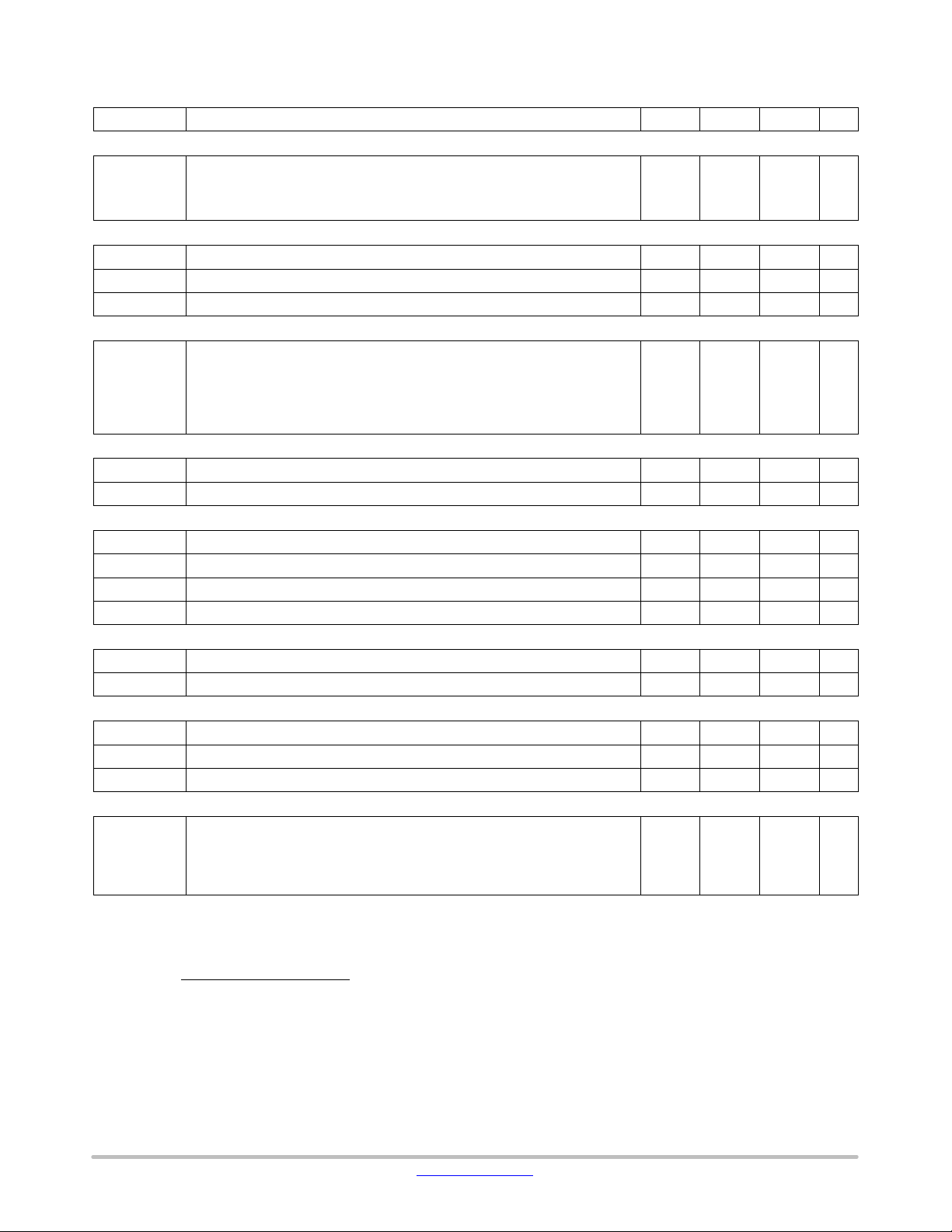
MARKING DIAGRAM
8
54Bxx
ALYW
G
1
xx = 65, 133 or 200
A = Assembly Location
L = Wafer Lot
Y = Year
W = Work Week
G = Pb−Free Package
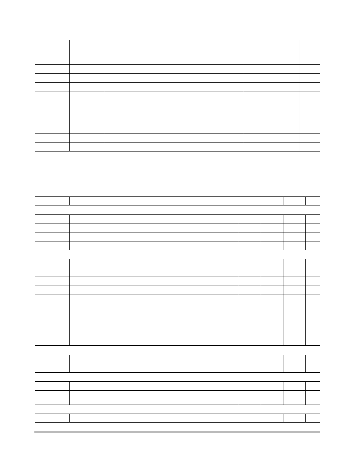
PIN CONNECTIONS
Ground
Brown−Out
V
CS
M
1
2
3
4
(Top View)
Driver
8
V
7
CC
Feedback
6
V
5
control
Safety Features
• Inrush Currents Detection
• Overvoltage Protection
• Undervoltage Detection for Open Loop Detection or Shutdown
• Brown−Out Detection
• Soft−Start
• Accurate Overcurrent Limitation
• Overpower Limitation
Typical Applications
• Flat TVs, PC Desktops
• AC Adapters
• White Goods, other Off−line SMPS
© Semiconductor Components Industries, LLC, 2016
March, 2021 − Rev. 6
1 Publication Order Number:
ORDERING INFORMATION
Device Package Shipping
NCP1654BD65R2G 2500 /
NCP1654BD133R2G 2500 /
NCP1654BD200R2G 2500 /
†For information on tape and reel specifications,
including part orientation and tape sizes, please
refer to our Tape and Reel Packaging Specification
Brochure, BRD8011/D.
SO−8
(Pb−Free)
SO−8
(Pb−Free)
SO−8
(Pb−Free)
Tape & Reel
Tape & Reel
Tape & Reel
NCP1654/D
†
Page 2
NCP1654
MAXIMUM RATINGS TABLE
Symbol Pin Rating Value Unit
DRV 8 Output Drive Capability − Source
Output Drive Capability − Sink
V
CC
7 Power Supply Voltage, VCC pin, continuous voltage −0.3, +20 V
7 Transient Power Supply Voltage, duration < 10 ms, IVCC < 10 mA +25 V
Vin 2, 3, 4, 5, 6 Input Voltage −0.3, +10 V
Power Dissipation and Thermal Characteristics
D suffix, Plastic Package, Case 751
PD(SO)
R
q
JA
T
T
Jmax
T
Smax
T
Lmax
(SO)
J
Maximum Power Dissipation @ TA = 70°C
Thermal Resistance Junction−to−Air
Operating Junction Temperature Range −40 to +125 °C
Maximum Junction T
emperature
Storage Temperature Range −65 to +150 °C
Lead Temperature (Soldering, 10 s) 300 °C
Stresses exceeding those listed in the Maximum Ratings table may damage the device. If any of these limits are exceeded, device functionality
should not be assumed, damage may occur and reliability may be affected.
1. This device series contains ESD protection and exceeds the following tests:
Human Body Model (HBM) 2000 V per JEDEC standard JESD22, Method A114E
Machine Model (MM) 200 V (except pin#7 which complies 150 V) per JEDEC standard JESD22, Method A115A.
2. This device contains Latch−up Protection and exceeds ±100 mA per JEDEC Standard JESD78.
−1.5
+1.5
450
178
mW
°C/W
150 °C
A
TYPICAL ELECTRICAL CHARACTERISTICS TABLE (V
= 15 V, TJ from −40°C to +125°C, unless otherwise specified) (Note 3)
CC
Symbol Rating Min Typ Max Unit
GATE DRIVE SECTION
R
OH
R
OL
T
r
T
f
Source Resistance @ I
Sink Resistance @ I
= 100 mA − 9.0 20 W
source
= −100 mA − 6.6 18 W
sink
Gate Drive Voltage Rise Time from 1.5 V to 13.5 V (C
Gate Drive Voltage Fall Time from 13.5 V to 1.5 V (C
= 2.2 nF) − 60 − ns
L
= 2.2 nF) − 40 − ns
L
REGULATION BLOCK
V
REF
I
EA
G
EA
IBpin6 Pin 6 Bias Current @ VFB = V
V
control
V
control(max)
V
control(min)
DV
control
V
L / V
OUT
H
L / V
OUT
I
BOOST
Voltage Reference 2.425 2.5 2.575 V
Error Amplifier Current Capability − ±28 − mA
Error Amplifier Gain 100 200 300 mS
REF
−500 − 500 nA
Pin5 Voltage
Maximum Control Voltage @ V
Minimum Control Voltage @ V
REF
REF
DV
Ratio (V
Ratio (V
control
= V
control(max)
Low Detect Thresold / V
OUT
Low Detect Hysteresis / V
OUT
Pin 5 Source Current when (V
− V
= 2 V
FB
= 3 V
FB
control(min)
) 94 95 96 %
REF
) − 0.5 − %
REF
Low Detect) is activated 190 228 260 mA
OUT
2.7
−
−
3.6
0.6
3.0
−
−
3.3
CURRENT SENSE BLOCK
V
I
S(OCP)
S
Current Sense Pin Offset Voltage, (ICS = 100 mA) − 10 − mV
Overcurrent Protection Threshold 185 200 215 mA
POWER LIMITATION BLOCK
I
x V
CS
I
CS(OPL1)
I
CS(OPL2)
Overpower Limitation Threshold − 200 − mVA
BO
Overpower Current Threshold (VBO = 0.9 V, VM = 3 V)
Overpower Current Threshold (VBO = 2.67 V, VM = 3 V)
186
62
222
75
308
110
PWM BLOCK
Dcycle Duty Cycle Range − 0−97 − %
V
mA
www.onsemi.com
2
Page 3
NCP1654
TYPICAL ELECTRICAL CHARACTERISTICS TABLE (V
= 15 V, TJ from −40°C to +125°C, unless otherwise specified) (Note 3)
CC
Symbol UnitMaxTypMinRating
OSCILLATOR / RAMP GENERATOR BLOCK
fsw Switching Frequency
65 kHz
133 kHz
200 kHz
58
120
180
65
133
200
146
220
kHz
72
BROWN−OUT DETECTION BLOCK
V
V
BOH
BOL
I
IB
Brown−Out Voltage Threshold (rising) 1.22 1.30 1.38 V
Brown−Out Voltage Threshold (falling) 0.65 0.7 0.75 V
Pin 4 Input Bias Current @ VBO = 1 V −500 − 500 nA
CURRENT MODULATION BLOCK
I
M1
I
M2
Multiplier Output Current (V
Multiplier Output Current (V
(@ 0 125°C)
control
control
= V
= V
control(max)
control(max)
, VBO = 0.9 V, I
, VBO = 0.9 V, I
(@ −40 125°C)
I
M3
I
M4
Multiplier Output Current (V
Multiplier Output Current (V
control
control
= V
= V
control(min)
control(min)
+ 0.2 V, VBO = 0.9 V, I
+ 0.2 V, VBO = 0.9 V, I
CS
= 25 mA)
CS
= 75 mA)
CS
CS
= 25 mA
= 75 mA
1.5
1.5
−
−
−
1.9
4.7
4.7
28.1
84.4
8.8
9.8
−
mA
−
−
OVERVOLTAGE PROTECTION
V
OVP
T
/ V
OVP
Ratio (Overvoltage Threshold / V
REF
Propagation Delay (VFB – 107% V
) 103 105 107 %
REF
) to Drive Low − 500 − ns
REF
UNDERVOLTAGE PROTECTION / SHUTDOWN
V
UVP(on)/VREF
V
UVP(off)/VREF
V
UVP(H)
T
UVP
UVP Activate Threshold Ratio (TJ = 0°C to +105°C) 4 8 12 %
UVP Deactivate Threshold Ratio (TJ = 0°C to +105°C) 6 12 18 %
UVP Lockout Hysteresis − 4 − %
Propagation Delay (VFB < 8% V
) to Drive Low − 500 − ns
REF
THERMAL SHUTDOWN
T
SD
H
SD
Thermal Shutdown Threshold 150 − − °C
Thermal Shutdown Hysteresis − 30 − °C
VCC UNDERVOLTAGE LOCKOUT SECTION
V
CC(on)
V
CC(off)
V
CC(H)
Start−Up Threshold (Undervoltage Lockout Threshold, VCC rising) 9.6 10.5 11.4 V
Disable Voltage after Turn−On (Undervoltage Lockout Threshold, VCC falling) 8.25 9.0 9.75 V
Undervoltage Lockout Hysteresis 1.0 1.5 − V
DEVICE CONSUMPTION
Power Supply Current:
I
STUP
I
CC1
I
CC2
I
STDN
Start−Up (@ VCC = 9.4 V)
Operating (@ VCC = 15 V, no load, no switching)
Operating (@ VCC = 15 V, no load, switching)
Shutdown Mode (@ VCC = 15 V and V
FB
= 0 V)
−
−
−
−
−
3.7
4.7
300
75
5.0
6.0
400
mA
mA
mA
mA
Product parametric performance is indicated in the Electrical Characteristics for the listed test conditions, unless otherwise noted. Product
performance may not be indicated by the Electrical Characteristics if operated under different conditions.
3. The above specification gives the targeted values of the parameters. The final specification will be available once the complete circuit
characterization has been performed.
I
V
cs
NOTE:
IM+
4 ǒV
control
* V
BO
control(min)
Ǔ
www.onsemi.com
3
Page 4

NCP1654
DETAILED PIN DESCRIPTIONS
Pin Symbol Name Function
1 GND Ground −
2 V
in
3 CS Current Sense
4 V
5 V
6 V
7 V
BO
control
FB
CC
8 DRV Drive Output The high current capability of the totem pole gate drive (±1.5 A) makes it suitable to effectively
Multiplier
Voltage
This pin provides a voltage VM for the PFC duty cycle modulation. The input impedance of the
PFC circuits is proportional to the resistor RM externally connected to this pin. The device
operates in average current mode if an external capacitor CM is connected to the pin.
Otherwise, it operates in peak current mode.
This pin sources a current ICS which is proportional to the inductor current IL. The sense
Input
current I
modulation. When ICS goes above 200 mA, OCP is activated and the Drive Output is disabled.
is for overcurrent protection (OCP), overpower limitation (OPL) and PFC duty cycle
CS
Brown−Out / In Connect a resistor network among the rectified input voltage, BO pin, and ground. And connect
a capacitor between BO pin and ground. BO pin detects a voltage signal proportional to the
average input voltage.
When VBO goes below V
(brown−out), turns off the output driver and keeps it in low state until VBO exceeds V
, the circuit that detects too low input voltage conditions
BOL
BOH
This signal which is proportional to the RMS input voltage Vac is also for overpower limitation
(OPL) and PFC duty cycle modulation.
Control Voltage /
Soft−Start
Feed−Back /
Shutdown
The voltage of this pin V
external type−2 compensation components to limit the V
to achieve near unity power factor.
The device provides no output when V
increases slowly (soft−start).
directly controls the input impedance. This pin is connected to
control
control
< V
control(min)
bandwidth typically below 20 Hz
control
. When it starts operation, the power
This pin receives a feedback signal VFB that is proportional to the PFC circuits output voltage.
This information is used for both the output regulation, the overvoltage protection (OVP), and
output undervoltage protection (UVP) to protect the system from damage at feedback
abnormal situation.
When VFB goes above 105% V
When VFB goes below 8% V
Supply Voltage This pin is the positive supply of the IC. The circuit typically starts to operate when V
exceeds 10.5 V and turns off when VCC goes below 9 V. After start−up, the operating range is
, OVP is activated and the Drive Output is disabled.
REF
, the device enters a low−consumption shutdown mode.
REF
CC
9 V up to 20 V.
drive high gate charge power MOSFET.
.
www.onsemi.com
4
Page 5
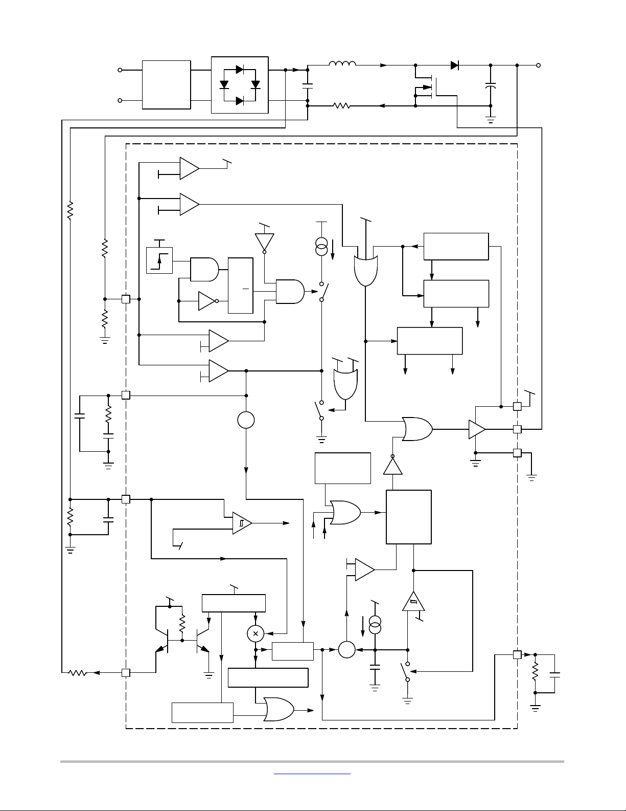
AC
Input
EMI
Filter
NCP1654
V
in
I
IN
+
−
in
L
C
filter
R
SENSE
I
L
I
L
+
C
bulk
Output
Voltage
(V
OUT
)
R
boU
R
R
Vcontrol
C
P
R
boL
fbU
fbL
C
+
OVP
-
105% Vref
UVP
-
+
8% Vref with 4% Vref
Vdd
Hysteresis
Soft Start
OPL
Vdd
200 mA
BO
UVLO
Undervoltage
Lock−Out
S
FB
6
Q
R
Reference
Block
Vref
-
Vref
+
Vout Low Detect
OTA
-
+
±28 mA
+
UVP BO
95% Vref
5
R
Z
Vcontrol(min)
C
Z
Thermal
Off
Bias Block
Iref Vdd
Output
Buffer
Vcc
7
8
DRV
1
GND
Shutdown
BO
BO
4
-
BO
+
VboH / VboL
VboH = 1.3 V, VboL = 0.7 V
Vdd
OL
OVP
Vref
Vramp
-
+
Vdd
Current Mirror
Ics
Ics
Vbo
Fault
Vdd
Q
PWM
R
Latch
RS
Iref
+
-
Vref/10% Vref
Ics
R
CS
CS
3
Ics*Vbo > 200 mVA
OPL
Division
OL
Ics > 200 mA
+
C1
S1
65/133/200 kHz
Oscillator
Im = (Ics*Vbo) / (4*(Vcontrol − Vcontrol(min))
Vm
R
2
M
C
M
OCP
Figure 1. Functional Block Diagram
www.onsemi.com
5
Page 6
NCP1654
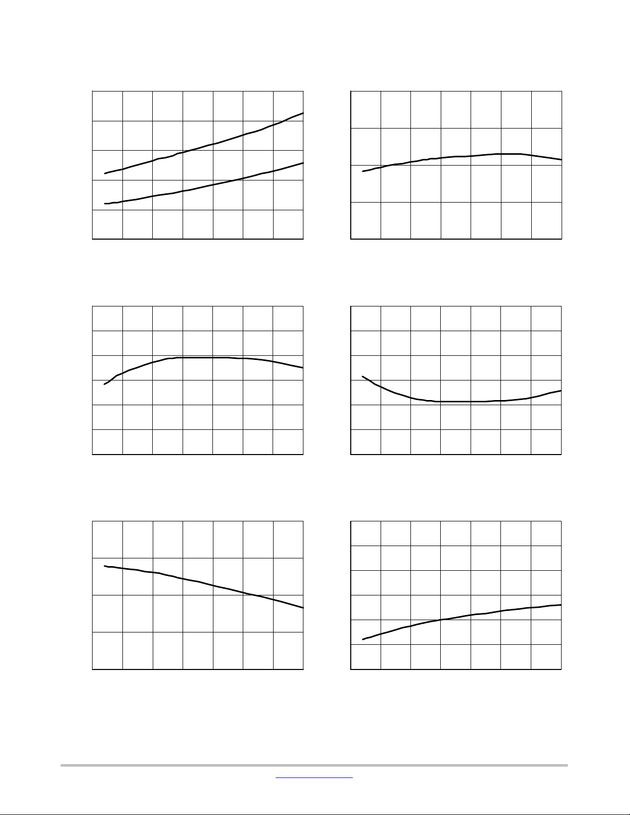
TYPICAL CHARACTERISTICS
10
8
6
, GATE DRIVE
OL
4
& R
RESISTANCE (W)
OH
R
2
0
32
30
28
(A)
26
EA_source
I
24
2.60
(V)
REF
V
2.55
2.50
2.45
2.40
Figure 3. Reference Voltage vs. Temperature
R
OH
R
OL
10075 12550250−25−50
TJ, JUNCTION TEMPERATURE (°C) TJ, JUNCTION TEMPERATURE (°C)
Figure 2. Gate Drive Resistance vs.
Temperature
−20
−22
−24
(A)
−26
EA_sink
I
−28
1251007550250−25−50
22
20
TJ, JUNCTION TEMPERATURE (°C) TJ, JUNCTION TEMPERATURE (°C)
10075 12550250−25−50
Figure 4. Source Current Capability of the
Error Amplifier vs. Temperature
300
250
(mS)
200
EA
G
150
100
TJ, JUNCTION TEMPERATURE (°C) TJ, JUNCTION TEMPERATURE (°C)
1251007550250−25−50 10075 12550250−25−50
−30
−32
150
100
50
0
pin6 (nA)
B
I
−50
−100
−150
Figure 5. Sink Current Capability of the Error
Amplifier vs. Temperature
Figure 6. Error Amplifier Gain vs. Temperature Figure 7. Feedback Pin Current vs.
Temperature (@V
fb
= V
REF
10075 12550250−25−50
)
www.onsemi.com
6
Page 7
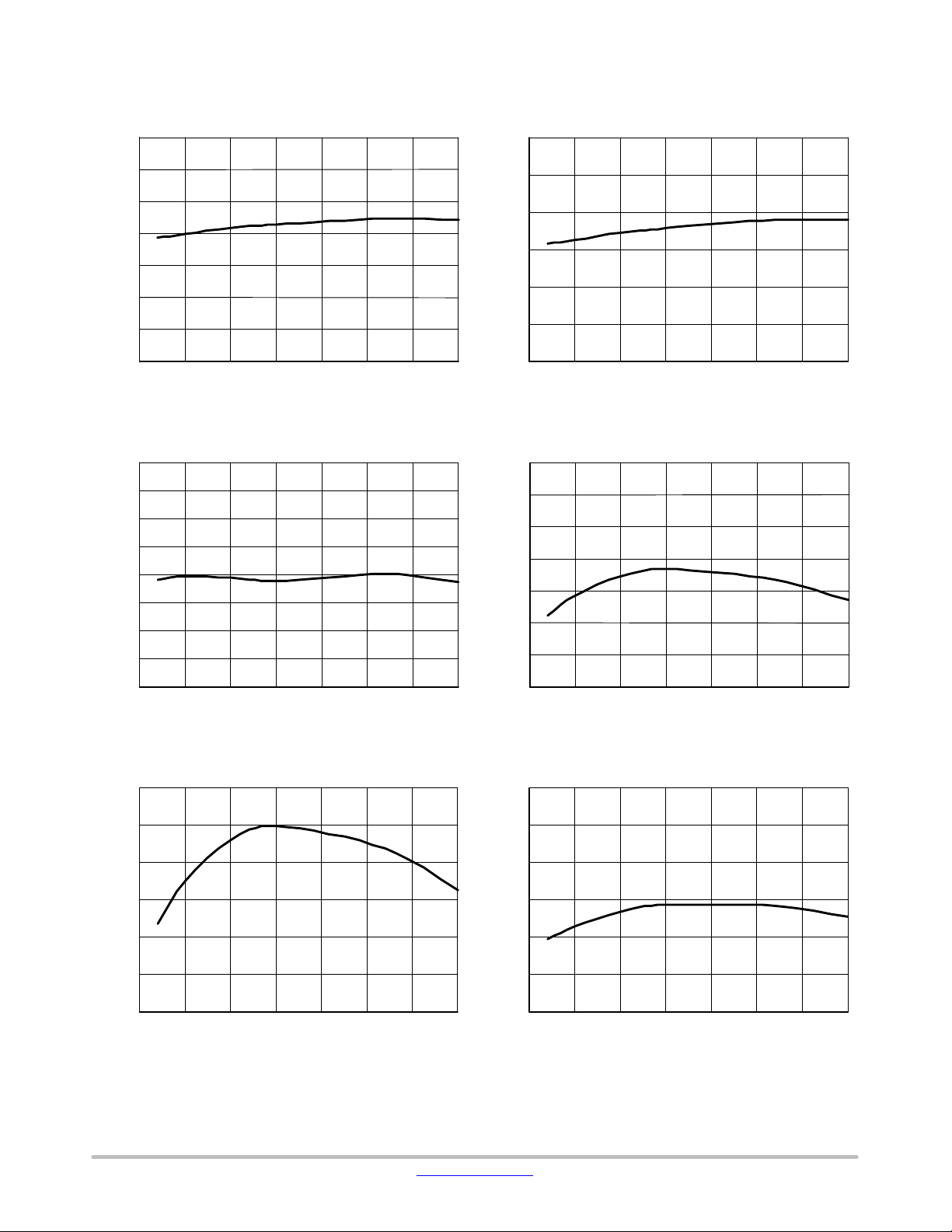
NCP1654
TYPICAL CHARACTERISTICS
4.0
3.9
3.8
(V)
3.7
3.6
CONTROL(max )
V
3.5
3.4
3.3
95.1
95.0
94.9
94.8
(%)
REF
94.7
/ V
94.6
outL
V
94.5
94.4
94.3
Figure 10. Ratio (V
215
3.3
3.2
3.1
(V)
3.0
CONTROL
2.9
DV
2.8
10075 12550250−25−50
TJ, JUNCTION TEMPERATURE (°C) TJ, JUNCTION TEMPERATURE (°C)
Figure 8. V
Maximum Voltage vs.
control
Temperature
1007550 125250−25−50
TJ, JUNCTION TEMPERATURE (°C) TJ, JUNCTION TEMPERATURE (°C)
Low Detect Threshold /
OUT
) vs. Temperature
V
REF
2.7
260
250
240
230
(mA)
220
Boost
I
210
200
190
306
−50
Figure 9. V
0−25
Maximum Swing (DV
control
vs. Temperature
Figure 11. Pin 5 Source Current when (V
Low Detect) is Activated vs. Temperature
10075 1255025
CONTROL
10075 12550250−25−50
OUT
)
210
205
(mA)
200
S(OCP)
I
195
190
185
−50 0−25 10075 1255025−50
0−25
TJ, JUNCTION TEMPERATURE (°C) TJ, JUNCTION TEMPERATURE (°C)
10075 1255025
Figure 12. Over−Current Protection Threshold
vs. Temperature
www.onsemi.com
286
266
(mA)
246
CS(OPL1)
I
226
206
186
Figure 13. Over−Power Current Threshold
= 0.9 V & Vm = 3 V) vs. Temperature
(@V
BO
7
Page 8
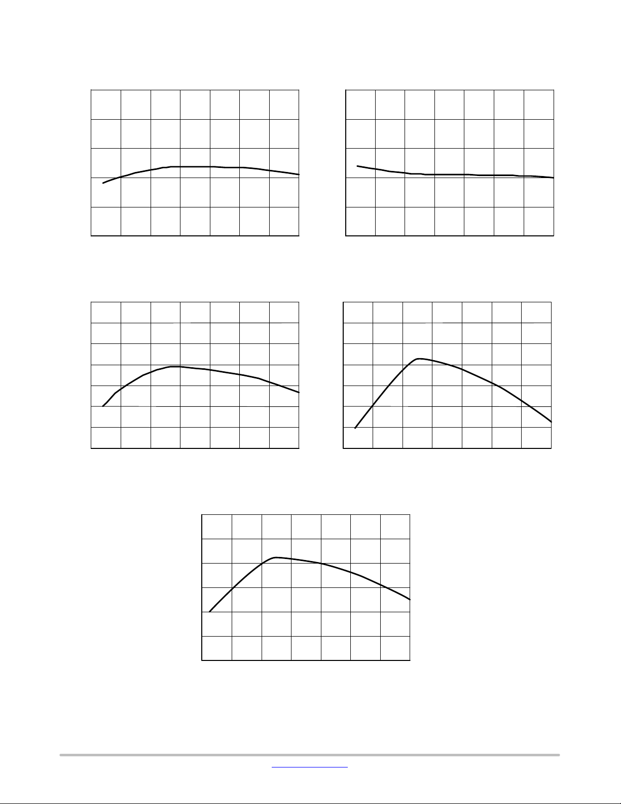
NCP1654
TYPICAL CHARACTERISTICS
110
100
90
(mA)
80
CS(OPL2)
I
70
60
72
70
68
66
(kHz)
64
SW
f
62
100
99
98
97
96
MAXIMUM DUTY CYCLE (%)
140
138
136
134
(kHz)
132
SW
f
130
95
Figure 15. Maximum Duty Cycle vs.
Temperature
1251007550250−25−50
TJ, JUNCTION TEMPERATURE (°C) TJ, JUNCTION TEMPERATURE (°C)
Figure 14. Over−Power Current Threshold
= 2.67 V & Vm = 3 V) vs. Temperature
(@V
BO
1251007550250−25−50
60
58
TJ, JUNCTION TEMPERATURE (°C)
Figure 16. Switching Frequency vs.
Temperature (65 kHz Version)
210
205
200
195
(kHz)
SW
f
190
185
180
TJ, JUNCTION TEMPERATURE (°C)
Figure 18. Switching Frequency vs.
Temperature (200 kHz Version)
128
10075 12550250−25−50
126
10075 12550250−25−50
TJ, JUNCTION TEMPERATURE (°C)
Figure 17. Switching Frequency vs.
Temperature (133 kHz Version)
10075 12550250−25−50
www.onsemi.com
8
Page 9

NCP1654
5
TYPICAL CHARACTERISTICS
(V)
BOH
V
(mA)
m2
I
1.40
1.35
1.30
1.25
1.20
7.5
6.5
5.5
4.5
10075 12550250−25−50
TJ, JUNCTION TEMPERATURE (°C)
Figure 19. Brown−Out Voltage Threshold
(Rising) vs. Temperature
(L)
BOL
V
(V)V
OVP
V
0.75
0.70
0.65
10075 12550250−25−50
TJ, JUNCTION TEMPERATURE (°C)
Figure 20. Brown−Out Voltage Threshold
(Falling) vs. Temperature
2.66
2.64
2.62
(%)
REF
/ V
OVP
V
3.5
2.5
TJ, JUNCTION TEMPERATURE (°C)
Figure 21. Multiplier Output Current (V
V
CONTROL(max)
, Vbo = 0.9 V, ICS = 75 mA) vs.
Temperature
107
106
105
104
103
TJ, JUNCTION TEMPERATURE (°C)
control
10075 12550250−25−50
2.60
1251007550250−25−50
=
2.58
TJ, JUNCTION TEMPERATURE (°C)
Figure 22. Over Voltage Threshold vs.
50250−25−50
10075 12
Temperature
16
(%)
14
REF
12
/ V
10
UVP(off)
and V
REF
/ V
UVP(on)
8
6
4
2
0
TJ, JUNCTION TEMPERATURE (°C)
10075 12550250−25−50
Figure 23. Ratio (Over Voltage Threshold /
) vs. Temperature
V
REF
www.onsemi.com
Figure 24. UVP Activate and Deactivate
Threshold Ratio vs. Temperature
9
Page 10

NCP1654
5
TYPICAL CHARACTERISTICS
(V)
CC(on)
V
(V)
CC(H)
V
11.4
11.2
11.0
10.8
10.6
10.4
10.2
10.0
9.8
9.6
2.0
1.8
1.6
1.4
TJ, JUNCTION TEMPERATURE (°C)
Figure 25. VCC Start−Up Threshold (V
Rising) vs. Temperature
9.7
9.5
9.3
9.1
(V)
8.9
CC(off)
V
8.7
8.5
10075 12550250−25−50
CC
8.3
TJ, JUNCTION TEMPERATURE (°C)
Figure 26. V
50
40
30
(mA)
STUP
20
I
Disable Voltage after Turn−On
CC
Falling) vs. Temperature
(V
CC
50250−25−50
10075 12
1.2
1.0
TJ, JUNCTION TEMPERATURE (°C)
1251007550250−25−50
Figure 27. VCC UVLO Hysteresis vs.
Temperature
400
350
(mA)
300
STDN
I
250
200
TJ, JUNCTION TEMPERATURE (°C)
1251007550250−25−50
Figure 29. Supply Current in Shutdown Mode
vs. Temperature
10
0
Figure 28. Supply Current in Startup Mode vs.
4
3
I
2
1
OPERATING CURRENT (mA)
0
CC1
Figure 30. Operating Supply Current vs.
TJ, JUNCTION TEMPERATURE (°C)
Temperature
I
, No Load, Switching
CC2
, No Load, No Switching
TJ, JUNCTION TEMPERATURE (°C)
Temperature
1251007550250−25−50
1251007550250−25−50
www.onsemi.com
10
Page 11

NCP1654
Detailed Operating Description
Introduction
The NCP1654 is a PFC driver designed to operate in
fixed frequency, continuous conduction mode. The fixed
frequency operation eases the compliance with EMI
standard and the limitation of the possible radiated noise
that may pollute surrounding systems. In addition,
continuous conduction operation reduces the application
di/dt and their resulting interference. More generally, the
NCP1654 is an ideal candidate in systems where
cost−effectiveness, reliability and high power factor are the
key parameters. It incorporates all the necessary features to
build a compact and rugged PFC stage:
• Compactness and Flexibility: housed in a SO8
package, the NCP1654 requires a minimum of
external components. In particular, the circuit scheme
simplifies the PFC stage design and eliminates the
need for any input voltage sensing. In addition, the
circuit offers some functions like the Brown−Out or
the true power limiting that enable the optimizations
of the PFC design,
• Low Consumption and Shutdown Capability: the
NCP1654 is optimized to exhibit consumption as
small as possible in all operation modes. The
consumed current is particularly reduced during the
start−up phase and in shutdown mode so that the PFC
stage power losses are extremely minimized when the
circuit is disabled. This feature helps meet the more
stringent stand−by low power specifications. Just
ground the Feed−back pin to force the NCP1654 in
shutdown mode,
• Safety Protections: the NCP1654 permanently monitors
the output voltage, the coil current and the die
temperature to protect the system from possible
over−stresses. Integrated protections (Overvoltage
protection, coil current limitation, thermal shutdown...)
make the PFC stage extremely robust and reliable:
− Maximum Current Limit: the circuit permanently
senses the coil current and immediately turns off the
power switch if it is higher than the set current limit.
The NCP1654 also prevents any turn on of the
power switch as long as the coil current is not below
its maximum permissible level. This feature protects
the MOSFET from possible excessive stress that
could result from the switching of a current higher
than the one the power switch is dimensioned for. In
particular, this scheme effectively protects the PFC
stage during the start−up phase when large in−rush
currents charge the output capacitor.
− Undervoltage Protection for Open Loop Protection
or Shut−down: the circuit detects when the
feed−back voltage goes below than about 8% of the
regulation level. In this case, the circuit turns off and
its consumption drops to a very low value. This
feature protects the PFC stage from starting
operation in case of low AC line conditions or in
case of a failure in the feed−back network (i.e. bad
connection).
− Fast Transient Response: given the low bandwidth
of the regulation block, the output voltage of PFC
stages may exhibit excessive over or under−shoots
because of abrupt load or input voltage variations
(e.g. at start up). If the output voltage is too far from
the regulation level:
Overvoltage Protection: NCP1654 turns off the
power switch as soon as V
threshold (105% of the regulation level). Hence
a cost & size effective bulk capacitor of lower
voltage rating is suitable for this application,
Dynamic Response Enhancer: NCP1654
drastically speeds up the regulation loop by its
internal 200ĂmA enhanced current source when the
output voltage is below 95% of its regulation level.
− Brown−Out Detection: the circuit detects low AC
line conditions and disables the PFC stage in this
case. This protection mainly protects the power
switch from the excessive stress that could damage it
in such conditions,
− Over−Power Limitation: the NCP1654 computes the
maximum permissible current in dependence of the
average input voltage measured by the brown−out
block. It is the second OCP with a threshold that is
line dependent. When the circuit detects an
excessive power transfer, it resets the driver output
immediately,
− Thermal Shutdown: an internal thermal circuitry
disables the circuit gate drive and then keeps the
power switch off when the junction temperature
exceeds 150°C typically. The circuit resumes
operation once the temperature drops below about
120°C (30°C hysteresis),
− Soft Start: V
activates, or Undervoltage protection activates, and
no drive is provided.
At start up, the “200 mA enhanced current source” is
disabled. So there is only 28 mA to charge the
compensation components, and makes V
gradually. This is to obtain a slow increasing duty
cycle and hence reduce the voltage and current
stress on the MOSFET. Hence it provides a soft−start
feature.
is pulled low brown−out detection
control
exceeds the OVP
out
control
raise
• Output Stage Totem Pole: the NCP1654 incorporates
a ±1.5A gate driver to efficiently drive TO220 or
TO247 power MOSFETs.
www.onsemi.com
11
Page 12

NCP1654
PRINCIPLE OF NCP1654 SCHEME
CCM PFC Boost
A CCM PFC boost converter is shown in Figure 31. The
input voltage is a rectified 50 ro 60 Hz sinusoidal signal.
The MOSFET is switching at a high frequency (typically
65/133/200 kHz in NCP1654) so that the inductor current
IL basically consists of high and low−frequency
components.
Filter capacitor C
is an essential and very small value
filter
capacitor in order to eliminate the high−frequency
component of the inductor IL. This filter capacitor cannot
be too bulky because it can pollute the power factor by
distorting the rectified sinusoidal input voltage.
I
in
V
in
Figure 31. CCM PFC Boost Converter
PFC Methodology
L
I
L
C
filter
R
SENSE
+
C
Output
Voltage
bulk
V
out
The NCP1654 uses a proprietary PFC methodology
particularly designed for CCM operation. The PFC
methodology is described in this section.
I
L
I
in
The input filter capacitor C
and the front−ended EMI
filter
filter absorbs the high−frequency component of inductor
current IL. It makes the input current I
a low−frequency
in
signal only of the inductor current.
Iin+ I
L*50
(eq. 2)
where
I
is the input AC current.
in
is the inductor current.
I
L
I
supposes a 50 Hz operation. The suffix 50 means
L−50
it is with a 50 Hz bandwidth of the original I
.
L
From (Equation 1) and (Equation 2), the input
impedance Z
is formulated.
in
V
Zin+
I
in
T * t
in
+
V
out
1
T
I
L*50
(eq. 3)
where Zin is input impedance.
Power factor is corrected when the input impedance Z
in (Equation 3) is constant or varies slowly in the 50 or 60
Hz bandwidth.
V
M
V
ref
PFC Modulation
-
+
V
ramp
Clock
RSQ
C
ramp
I
ch
01
V
ref
+
in
t
1
t
2
T
Time
Figure 32. Inductor Current in CCM
As shown in Figure 32, the inductor current IL in a
switching period T includes a charging phase for duration
t1 and a discharging phase for duration t2. The voltage
conversion ratio is obtained in (Equation 1).
t1) t
V
out
V
in
Vin+
+
T * t
T
2
T
+
t
T * t
2
1
V
out
1
(eq. 1)
where
V
is the output voltage of PFC stage,
out
Vin is the rectified input voltage,
T is the switching period,
t1 is the MOSFET on time, and
t2 is the MOSFET off time.
V
ramp
V
M
V
without
M
Filtering
Clock
Latch Set
Latch Reset
Output
Inductor
Current
Figure 33. PFC Duty Modulation and Timing Diagram
The PFC modulation and timing diagram is shown in
Figure 33. The MOSFET on time t1 is generated by the
intersection of reference voltage V
V
. A relationship in (Equation 4) is obtained.
ramp
V
ramp
+ Vm)
C
Icht
ramp
and ramp voltage
REF
1
+ V
REF
(eq. 4)
where
www.onsemi.com
12
Page 13

NCP1654
p
V
is the internal ramp voltage, the positive input of the
ramp
PFC modulation comparator,
Vm is the multiplier voltage appearing on Vm pin,
Ich is the internal charging current,
C
is the internal ramp capacitor, and
ramp
V
is the internal reference voltage, the negative input of
REF
the PFC modulation comparator.
, C
I
ch
switching frequency. Hence the charging current Ich is
specially designed as in (Equation 5). The multiplier
voltage Vm is therefore expressed in terms of t1 in
(Equation 6).
Vm+ V
From (Equation 3) and (Equation 6), the input impedance
Zin is re−formulated in (Equation 7).
Because V
the multiplier voltage Vm is designed to be proportional to
the I
L−50
It is illustrated in Figure 34.
ramp
REF
, and V
t
*
C
ram
and V
REF
also act as the ramp signal of
REF
C
V
ramp
1
Ich+
C
V
ramp
T
Zin+
V
are roughly constant versus time,
out
REF
V
REF
REF
T
V
out
L*50
T * t
REF
+ V
m
I
(eq. 5)
1
T
(eq. 6)
(eq. 7)
in order to have a constant Zin for PFC purpose.
Vm+
4(V
control
PFC Duty
Modulation
RMIcsV
* V
CONTROL(min)
bo
V
)
I
m
m
2
R
C
M
M
Figure 35. External Connection on the Multiplier
Voltage Pin
The multiplier voltage Vm is generated according to
(Equation 8).
R
IcsV
M
Vm+
4(V
control
* V
CONTROL(min)
bo
(eq. 8)
)
Where,
RM is the external multiplier resistor connected to Vm pin,
which is constant.
Vbo is the input voltage signal appearing on the BO pin,
which is proportional to the rms input voltage,
Ics is the sense current proportional to the inductor current
IL as described in (Equation 11).
V
is the control voltage signal, the output voltage of
control
Operational Trans−conductance Amplifier (OTA), as
described in (Equation 12).
RM directly limits the maximum input power capability
and hence its value affects the NCP1654 to operate in either
“follower boost mode” or “constant output voltage mode”.
V
in
I
in
I
L
V
M
Time
Time
Time
Figure 34. Multiplier Voltage Timing Diagram
It can be seen in the timing diagram in Figure 33 that V
originally consists of a switching frequency ripple coming
from the inductor current IL. The duty ratio can be
inaccurately generated due to this ripple. This modulation
is the so−called “peak current mode”. Hence, an external
capacitor CM connected to the multiplier voltage Vm pin is
essential to bypass the high−frequency component of Vm.
The modulation becomes the so−called “average current
mode” with a better accuracy for PFC.
V
in
R
boU
Vbo
R
boL
4
C
BO
-
+
V
boH
V
boH
BO
/ V
boL
= 1.3 V, V
Figure 36. External Connection on the Brown Out Pin
m
Refer to Figure 36,
Ǹ
Vbo+ KBO(Vin) + KBO@
R
KBO+
boL
R
) R
boU
boL
22
p
where
Vbo is the voltage on BO pin.
KBO is the decay ratio of Vin to Vbo.
<Vin> is the average voltage signal of Vin, the voltage
appearing on C
filter
.
Vac is the RMS input voltage.
V
boL
ac
+
= 0.7 V
(eq. 9)
(eq. 10)
www.onsemi.com
13
Page 14

R
is low side resistor of the dividing resistors between
boL
Vin and BO pin.
R
is upper side resistor of the dividing resistors between
boU
Vin and BO pin.
I
L
CS
I
CS
R
CS
R
SENSE
V
Figure 37. Current Sensing
+
CS
−
I
L
NCP1654
Gnd
+
NCP1654
Refer to Figure 37, sense current Ics is proportional to the
inductor current IL as described in (Equation 11). I
consists of the high−frequency component (that depends on
di/dt or inductor L) and low−frequency component (that is
I
L−50
where
R
SENSE
RCS is the offset resistor between CS pin and R
).
R
Ics+
SENSE
R
CS
is the sense resistor to sense IL.
L
I
L
(eq. 11)
SENSE
.
V
in
R
fbU
V
fb
V
R
C
6
control
5
Z
Z
V
REF
R
fbL
C
P
Figure 38. V
Refer to Figure 38, the Operational Trans−conductance
Amplifier (OTA) senses V
dividers, R
voltage, V
V
. The operating range of V
out
V
CONTROL(min)
and R
fbU
control
fbL
, depending on the output power and hence
to V
CONTROL(max)
via the feedback resistor
out
. The OTA constructs a control
is from
control
. The signal used for
PFC duty modulation is after decreasing a offset voltage,
V
CONTROL(min)
This control current I
that comes from the PFC output voltage V
varying signal. The bandwidth of I
, i.e. V
control−VCONTROL(min)
control
.
is a roughly constant current
that is a slowly
out
can be
control
additionally limited by inserting the external type−2
compensation components (that are RZ, CZ, and CP as
shown in Figure 38). It is recommended to limit f
is the bandwidth of V
control
(or I
), below 20 Hz
control
control
, that
typically to achieve power factor correction purpose.
The transformer of V
out
to V
is as described in
control
(Equation 12) if CZ is >> CP. GEA is the error amplifier gain.
out
+
R
R
@ GEAR
fbL
fbL
) R
Z
fbU
1 ) sRZC
@
sRZCZ(1 ) sRZCP)
Z
(eq. 12)
V
control
V
V
out
+
±20 mA
-
+
OTA
Low−Pass Filtering
control
+
V
To Vm Pin
CONTROL(min)
From (Equation 7) − (Equation 11), the input impedance
Zin is re−formulated in (Equation 13).
Ǹ
2
Zin+
2pRCS@ (V
When IL is equal to I
RMR
control
V
VacKBOI
out
SENSE
* V
CONTROL(min)
, (Equation 13) is re−formulated
L−50
L
) @ V
REFIL*50
in (Equation 14)
Ǹ
2
Zin+
2pRCS@ (V
RMR
control
SENSE
* V
V
VacK
out
CONTROL(min)
BO
) @ V
REF
The multiplier capacitor CM is the one to filter the
high−frequency component of the multiplier voltage Vm.
The high−frequency component is basically coming from
the inductor current IL. On the other hand, the filter
capacitor C
similarly removes the high−frequency
filter
component of inductor current IL. If the capacitors CM and
C
match with each other in terms of filtering capability,
filter
IL becomes I
. Input impedance Zin is roughly constant
L−50
over the bandwidth of 50 or 60 Hz and power factor is
corrected.
(eq. 13)
(eq. 14)
www.onsemi.com
14
Page 15

NCP1654
Input and output power (Pin and P
) are derived in (Equation 15) when the circuit efficiency η is obtained or assumed.
out
The variable Vac stands for the rms input voltage.
2
Pin+
(V
T
V
control
ac
Z
in
2pRCS@ (V
+
* V
CONTROL(min)
V
control
out
2pRCS@ (V
P
+ h Pin+ h
out
(V
T
control
* V
CONTROL(min)
V
out
Follower Boost
The “Follower Boost” is an operation mode where the
pre−converter output voltage stabilizes at a level that varies
linearly versus the ac line amplitude. This technique aims
at reducing the gap between the output and input voltages
to optimize the boost efficiency and minimize the cost of
the PFC stage (refer to MC33260 data sheet for more
details at http://www.onsemi.com ).
The NCP1654 operates in follower boost mode when
V
is constant, i.e. V
control
raises to its maximum value
control
2pRCS@ (V
P
+ h
out
2pR
@ DV
+ h
CS
2ǸRMR
CONTROL(max)
CONTROL
SENSE
@ V
V
out
* V
2ǸRMR
)V
ac
control
)V
ac
CONTROL(min)
SENSE
* V
CONTROL(min)
2ǸRMR
SENSE
V
CONTROL(max)
) @ V
V
K
out
BO
V
K
out
BO
REF
) @ V
@ V
REF
ac
@ V
ac
. Re−formulate (Equation 16) to become
(Equation 17) and (Equation 18) by replace V
V
CONTROL(max)
. If V
is constant based on
control
(Equation 15), for a constant load or power demand the
output voltage V
of the converter is proportional to the
out
rms input voltage Vac. It means the output voltage V
becomes lower when the rms input voltage Vac becomes
lower. On the other hand, the output voltage V
lower when the load or power demand becomes higher.
2ǸRMR
REF
K
BO
* V
CONTROL(min)
SENSE
@ V
ac
V
out
) @ V
K
BO
REF
@ V
ac
(eq. 15)
(eq. 16)
control
becomes
out
(eq. 17)
by
out
2pR
@ DV
V
+ h
out
CS
2ǸRMR
CONTROL
SENSEKBO
where
V
CONTROL(max)
DV
CONTROL
V
CONTROL(min)
is the maximum control voltage.
is the gap between V
CONTROL(max)
.
and
It is illustrated in Figure 39.
V
(Traditional Boost)
out
V
(Follower Boost)
out
V
in
Time
P
out
Time
Figure 39. Follower Boost Characteristics
Follower Boost Benefits
The follower boost circuit offers and opportunity to
reduce the output voltage V
voltage Vac is lower or the power demand P
whenever the rms input
out
is higher.
out
Because of the step−up characteristics of boost converter,
@ V
V
REF
ac
@
P
out
the output voltage V
will always be higher than the input
out
voltage Vin even though V
is reduced in follower boost
out
operation. As a result, the on time t1 is reduced. Reduction
of on time makes the loss of the inductor and power
MOSFET smaller. Hence, it allows cheaper cost in the
inductor and power MOSFET or allows the circuit
components to operate at a lower stress condition in most
of the time.
Reference Section
The internal reference voltage (V
) is trimmed to be
REF
±2% accurate over the temperature range (the typical value
is 2.5 V). V
V
also serves to build the thresholds of the fast transient
REF
is the reference used for the regulation.
REF
response, Overvoltage (OVP), brown out (BO), and
Undervoltage protections (UVP).
Output Feedback
The output voltage V
Vfb pin via the resistor divider (R
Figure 38. V
is regulated as described in (Equation 19).
out
V
out
of the PFC circuits is sensed at
out
+ V
REF
and R
fbL
R
) R
fbU
R
fbL
fbU
fbL
) as shown in
(eq. 18)
(eq. 19)
www.onsemi.com
15
Page 16

NCP1654
The feedback signal Vfb represents the output voltage
V
and will be used in the output voltage regulation,
out
Overvoltage protection (OVP), fast transient response, and
Undervoltage protection (UVP)
Output Voltage Regulation
NCP1654 uses a high gain Operational Trans−
conductance Amplifier (OTA) as error amplifier. Refer to
Figure 38, the output of OTA V
from V
CONTROL(min)
to V
CONTROL(max)
C
control
FB
operating range is
.
R
fbU
V
fb
6
R
fbL
V
control
5
105%
95%
V
REF
V
REF
V
REF
Fast Transient Response
Given the low bandwidth of the regulation block, the
output voltage of PFC stages may exhibit excessive over or
under−shoots because of abrupt load or input voltage
variations (such as start−up duration). As shown in
Figure 40, if the output voltage is out of regulation,
NCP1654 has 2 functions to maintain the output voltage
regulation.
V
out
+
Vdd
V
out
±20 mA
OTA
OVP
200 mA
Low Detect
-
+
-
+
-
+
Figure 40. OVP and Fast Transient Response
• Overvoltage Protection: When V
105% of V
REF
(i.e. V
> 105% of nominal output
out
is higher than
fb
voltage), the Driver output of the device goes low for
protection. The circuit automatically resumes
operation when Vfb becomes lower than 105% of
V
. If the nominal V
REF
is set at 390 V, then the
out
maximum output voltage is 105% of 390 V = 410 V.
Hence a cost & size effective bulk capacitor of lower
voltage rating is suitable for this application,
• Dynamic response enhancer: NCP1654 drastically
speeds up the regulation loop by its internal 200 mA
enhanced current source when the output voltage is
below 95% of its regulation level. Under normal
50
200 mA raises
0
V
rapidly
control
when Vfb is below
−50
95% V
−100
−150
PIN CURRENT (mA)
−200
−250
CONTROL
V
Figure 41. Vfb vs. Current Flowing in/out from V
REF
2 2.2 2.4 2.6 2.8 3
condition, the maximum sink and source of output
current capability of OTA is around 28 mA. Thanks to
the “V
95% V
V
low detect” block, when the V
out
, an extra 200 mA current source will raise
REF
rapidly. Hence prevent the PFC output from
control
is below
fb
dropping too low and improve the transient response
performance. The relationship between current
flowing in/out V
pin and Vfb is as shown in
control
Figure 41.
It is recommended to add a typical 100 pF capacitor C
decoupling capacitor next to feedback pin to prevent from
noise impact.
No DRV when
Vfb is above
105% V
REF
Vfb
Pin
control
FB
www.onsemi.com
16
Page 17

NCP1654
Soft Start
The block diagram and timing diagram of soft start
function are as shown in Figure 42 and Figure 43. The
device provides no output (or no duty ratio) when the
V
is lower than V
control
CONTROL(min)
. V
control
is pulled low
when:
• Brown−out, or
• Undervoltage Protection
When the IC recovers from one of the following
conditions; Undervoltage Lockout, Brown−out or
Undervoltage Protection, the 200 mA current source block
keeps off. Hence only the Operating Trans−conductance
Amplifier (OTA) raises the V
slowly. This is to obtain a slow increasing duty cycle and
hence reduce the voltage and current stress on the
MOSFET. A soft−start operation is obtained.
control
. And V
control
rises
Vdd
Off
Bias
Q
S
Q
R
Vfb
V
6
control
5
95%
V
REF
-
+
V
REF
-
+
OTA
Figure 42. Soft Start Block Diagram
V
Low Detect
out
±20 mA
UVPUVLOBO
Vdd
200 mA
UVLOBO
UVLO, BO, or UVP
Vdd
Vdd Rising
Vfb
Vout Low Detect
Set
Reset
Period I Period II
95% V
REF
Q
Figure 43. Soft Start Timing Diagram
www.onsemi.com
17
Page 18

NCP1654
Undervoltage Protection (UVP) for Open Loop
Protection or Shutdown
I
STDN
Shutdown
I
CC2
8% V
REF
Figure 44. Undervoltage Protection
As shown in Figure 44, when Vfb is less than 8% of V
12% V
Operating
V
REF
fb
REF
the device is shut down and consumes less than 400 mA.
The device automatically starts operation when the output
voltage goes above 12% of V
boost converter configuration, the output voltage V
. In normal situation of
REF
out
is
always greater than the input voltage Vin and the feedback
signal V
is always greater than 8% and 12% of V
fb
REF
to
enable NCP1654 to operate.
This Undervoltage Protection function has 2 purposes.
• Open Loop Protection − Protect the power stage from
damage at feedback loop abnormal, such as Vfb is
shorted to ground or the feedback resistor R
fbU
is
open.
• Shutdown mode − Disables the PFC stage and forces a
low consumption mode. This feature helps to meet
stringent stand−by specifications. Power Factor being
not necessary in stand−by, the PFC stage is generally
inhibited to save the pre−converter losses. To further
improve the stand−by performance, the PFC controller
should consume minimum current in this mode.
Current Sense
The device senses the inductor current I
sense scheme in Figure 37. The device maintains the
voltage at CS pin to be zero voltage (i.e., Vcs ≈ 0 V) so that
(Equation 11),
R
Ics+
SENSE
R
CS
IL,
can be formulated.
This scheme has the advantage of the minimum number
of components for current sensing. The sense current I
represents the inductor current IL and will be used in the
PFC duty modulation to generate the multiplier voltage
Vm, Over−Power Limitation (OPL), and Over−Current
Protection. (Equation 11) would insist in the fact that it
provides the flexibility in the R
SENSE
allows to detect in−rush currents.
by the current
L
choice and that it
Over−Current Protection (OCP)
Over−Current Protection is reached when Ics is larger
than I
(200 mA typical). The offset voltage of the CS
S(OCP)
pin is typical 10 mV and it is neglected in the calculation.
Hence, the maximum OCP inductor current threshold
I
is obtained in (Equation 20).
L(OCP)
I
L(OCP)
+
RCSI
R
S(OCP)
SENSE
+
R
R
SENSE
CS
@ 200 mA
(eq. 20)
When over−current protection threshold is reached, the
Drive Output of the device goes low. The device
automatically resumes operation when the inductor current
goes below the threshold.
Input Voltage Sense
,
The device senses the rms input voltage Vac by the
sensing scheme in Figure 45. Vbo senses the average
rectified input voltage Vin via the resistor divider. An
external capacitor CBO is to maintain the Vbo the average
value of Vin. Vbo is used for Brown−Out Protection, PFC
duty modulation and over−power limitation (OPL).
Brown−Out Protection
The device uses the Vbo signal to protect the PFC stage
from operating as the input voltage is lower than expected.
Re−formulate (Equation 9) to get (Equation 21). Refer to
Figure 45, Vin is different before and after the device
operating.
• Before the device operates, V
is equal to the peak
in
value of rms input voltage, Vac. Hence Vbo is as
described in (Equation 21).
R
Vbo+
boL
R
) R
boL
(Vin) +
boU
• After device operates, V
R
boL
R
) R
boL
is the rectified sinusoidal
in
boU
2ǸV
ac
(eq. 21)
input voltage. Thanks to CBO, Vbo is the average of
rectified input voltage. Hence Vbo decays to 2/p of the
peak value of rms input voltage Vac as described in
(Equation 22).
boU
Ǹ
22
p
V
ac
(eq. 22)
R
Vbo+
cs
boL
R
) R
boL
www.onsemi.com
18
Page 19

NCP1654
After Device OperatesBefore Device Operates
V
in
V
ac
IN
R
boU
R
boL
+
−
Vbo
4
C
BO
-
+
Figure 45. Brown−Out Protection
BO
V
V
boH
boH
/ V
boL
= 1.3 V, V
boL
+
= 0.7 V
Hence a larger hysteresis of the brown out comparator is
needed, which is 0.7 V typical in this device. When V
goes below than V
(0.7 V typical), the device turns off
BOL
the Drive output and keeps it off till Vbo exceeds V
bo
BOH
(1.3 V typical). When the device awakes after an off−state
(Undervoltage lockout or shutdown), the default threshold
is V
BOH
.
V
in
R
SENSE
RCS
ICS
CS
3
4
Vbo
Current Mirror
Figure 46. Over−Power Limitation
When the product (Ics ⋅ Vbo) is greater than a permissible
level 200 mVA, the device turns off the drive output so that
the input power is limited. The OPL is automatically
deactivated when the product (Ics ⋅ Vbo) is lower than the
200 mVA level. This 200 mVA level corresponds to the
approximated input power (IL ⋅ Vac) to be smaller than the
particular expression in (Equation 23).
IcsVbot 200 mVA
R
SENSE
ǒ
I
L
Ǔ
R
@ ǒ
CS
22ǸK
p
BO
@ V
Ǔt 200 mVA
ac
(eq. 23)
Overpower Limitation (OPL)
This is a second OCP with a threshold that is line
dependent. Sense current Ics represents the inductor current
IL and hence represents the input current approximately.
Input voltage signal Vbo represents the rms input voltage.
The product (Ics ⋅ Vbo) represents an approximated input
power (IL ⋅ Vac). It is illustrated in Figure 46.
+
I
L
R
L
SENSE
R
CS
OPL
>200 mVA?
ICS+ I
Bias the Controller
It is recommended to add a typical 1 nF to 100 nF
decoupling capacitor next to the Vcc pin for proper
operation. When the NCP1654 operates in follower boost
mode, the PFC output voltage is not always regulated at a
particular level under all application range of input voltage
and load power. It is not recommended to make a
low−voltage bias supply voltage by adding an auxiliary
winding on the PFC boost inductor. Alternatively, it is
recommended to get the Vcc biasing supply from the
2nd−stage power conversion stage.
@ Vact
I
L
R
SENSE
R
@ p
CS
@ K
BO
@ 50 2ǸmVA
www.onsemi.com
19
Page 20

NCP1654
Vcc Undervoltage LockOut (UVLO)
The device incorporates an Undervoltage Lockout block
to prevent the circuit from operating when Vcc is too low
in order to ensure a proper operation. An UVLO
comparator monitors Vcc pin voltage to allow the NCP1654
to operate when Vcc exceeds 10.5 V typically. The
State
OFF
comparator incorporates some hysteresis (1.5 V) to prevent
erratic operation as the Vcc crosses the threshold. When V
goes below the UVLO comparator lower threshold (9 V
typically), the circuit turns off. It is illustrated in Figure 47.
After startup, the operating range is between 9 V and 20 V.
ON
V
CC
cc
I
CC
<75 mA
V
CC(OFF)
Figure 47. Vcc Undervoltage LockOut (UVLO)
Thermal Shutdown
An internal thermal circuitry disables the circuit gate
drive and then keeps the power switch off when the junction
temperature exceeds 150°C. The output stage is then
6 mA
V
CC
V
CC(ON)
enabled once the temperature drops below typically 120°C
(i.e., 30°C hysteresis). The thermal shutdown is provided
to prevent possible device failures that could result from an
accidental overheating.
www.onsemi.com
20
Page 21

TB2
NCP1654
390 V
R1R21.8 M
1.8 M
L1
12
180 mF, 450 V
+
D1 MSR860G
SPP20N60S5
Q1
5
650 mH
2
C4
R4
10 k
R6 0.1
1N4148
D2
R5 10
R7
3.6 k
TB3
+15 V
0.1 mF
DRV
VCC
FB
Vcontrol
8765
NCP1654
IC1
1234
CS
GND
VM
BO
21
2.2 mF
R12
12 k
1 nF
C8
+
22 mFC9
C10
100 pF
R3
23.2 k
C12
C5
220 nF
R8
47 k
C6
5 A Fuse
AC Inlet
GBU8J
600 V
8 A
DB1
L3
F1
1
LN
+
−
C2
0.47 mF
150 mH
C1
0.47 mF
23
R10
0
C3
2 x 6.8 mHL2
TB1
0.1 mF
R9
3.3 M
R13
3.3 M
Figure 48. Application Schematic − 300 W 65 kHz
Power Factor Correction Circuit
R11
82.5 k
C7
0.47 mF
www.onsemi.com
21
Page 22

MECHANICAL CASE OUTLINE
PACKAGE DIMENSIONS
8
1
SCALE 1:1
B
−Y−
−Z−
H
−X−
A
58
S
1
4
G
D
0.25 (0.010) Z
M
SOLDERING FOOTPRINT*
7.0
0.275
Y
SXS
0.25 (0.010)
C
SEATING
PLANE
1.52
0.060
0.155
0.10 (0.004)
4.0
CASE 751−07
M
M
Y
N
SOIC−8 NB
ISSUE AK
K
X 45
_
M
J
MARKING DIAGRAM*
8
XXXXX
ALYWX
1
XXXXX = Specific Device Code
A = Assembly Location
L = Wafer Lot
Y = Year
W = Work Week
G = Pb−Free Package
8
XXXXX
ALYWX
G
1
IC
IC
(Pb−Free)
DATE 16 FEB 2011
NOTES:
1. DIMENSIONING AND TOLERANCING PER
ANSI Y14.5M, 1982.
2. CONTROLLING DIMENSION: MILLIMETER.
3. DIMENSION A AND B DO NOT INCLUDE
MOLD PROTRUSION.
4. MAXIMUM MOLD PROTRUSION 0.15 (0.006)
PER SIDE.
5. DIMENSION D DOES NOT INCLUDE DAMBAR
PROTRUSION. ALLOWABLE DAMBAR
PROTRUSION SHALL BE 0.127 (0.005) TOTAL
IN EXCESS OF THE D DIMENSION AT
MAXIMUM MATERIAL CONDITION.
6. 751−01 THRU 751−06 ARE OBSOLETE. NEW
STANDARD IS 751−07.
MILLIMETERS
DIMAMIN MAX MIN MAX
4.80 5.00 0.189 0.197
B 3.80 4.00 0.150 0.157
C 1.35 1.75 0.053 0.069
D 0.33 0.51 0.013 0.020
G 1.27 BSC 0.050 BSC
H 0.10 0.25 0.004 0.010
J 0.19 0.25 0.007 0.010
K 0.40 1.27 0.016 0.050
M 0 8 0 8
____
N 0.25 0.50 0.010 0.020
S 5.80 6.20 0.228 0.244
INCHES
GENERIC
8
XXXXXX
AYWW
1
Discrete
XXXXXX = Specific Device Code
A = Assembly Location
Y = Year
WW = Work Week
G = Pb−Free Package
8
XXXXXX
AYWW
1
Discrete
(Pb−Free)
G
0.6
0.024
1.270
0.050
SCALE 6:1
ǒ
inches
mm
Ǔ
*This information is generic. Please refer to
device data sheet for actual part marking.
Pb−Free indicator, “G” or microdot “G”, may
or may not be present. Some products may
not follow the Generic Marking.
*For additional information on our Pb−Free strategy and soldering
details, please download the ON Semiconductor Soldering and
Mounting Techniques Reference Manual, SOLDERRM/D.
STYLES ON PAGE 2
DOCUMENT NUMBER:
DESCRIPTION:
ON Semiconductor and are trademarks of Semiconductor Components Industries, LLC dba ON Semiconductor or its subsidiaries in the United States and/or other countries.
ON Semiconductor reserves the right to make changes without further notice to any products herein. ON Semiconductor makes no warranty, representation or guarantee regarding
the suitability of its products for any particular purpose, nor does ON Semiconductor assume any liability arising out of the application or use of any product or circuit, and specifically
disclaims any and all liability, including without limitation special, consequential or incidental damages. ON Semiconductor does not convey any license under its patent rights nor the
rights of others.
© Semiconductor Components Industries, LLC, 2019
98ASB42564B
SOIC−8 NB
Electronic versions are uncontrolled except when accessed directly from the Document Repository.
Printed versions are uncontrolled except when stamped “CONTROLLED COPY” in red.
PAGE 1 OF 2
www.onsemi.com
Page 23

STYLE 1:
PIN 1. EMITTER
2. COLLECTOR
3. COLLECTOR
4. EMITTER
5. EMITTER
6. BASE
7. BASE
8. EMITTER
STYLE 5:
PIN 1. DRAIN
2. DRAIN
3. DRAIN
4. DRAIN
5. GATE
6. GATE
7. SOURCE
8. SOURCE
STYLE 9:
PIN 1. EMITTER, COMMON
2. COLLECTOR, DIE #1
3. COLLECTOR, DIE #2
4. EMITTER, COMMON
5. EMITTER, COMMON
6. BASE, DIE #2
7. BASE, DIE #1
8. EMITTER, COMMON
STYLE 13:
PIN 1. N.C.
2. SOURCE
3. SOURCE
4. GATE
5. DRAIN
6. DRAIN
7. DRAIN
8. DRAIN
STYLE 17:
PIN 1. VCC
2. V2OUT
3. V1OUT
4. TXE
5. RXE
6. VEE
7. GND
8. ACC
STYLE 21:
PIN 1. CATHODE 1
2. CATHODE 2
3. CATHODE 3
4. CATHODE 4
5. CATHODE 5
6. COMMON ANODE
7. COMMON ANODE
8. CATHODE 6
STYLE 25:
PIN 1. VIN
2. N/C
3. REXT
4. GND
5. IOUT
6. IOUT
7. IOUT
8. IOUT
STYLE 29:
PIN 1. BASE, DIE #1
2. EMITTER, #1
3. BASE, #2
4. EMITTER, #2
5. COLLECTOR, #2
6. COLLECTOR, #2
7. COLLECTOR, #1
8. COLLECTOR, #1
STYLE 2:
PIN 1. COLLECTOR, DIE, #1
2. COLLECTOR, #1
3. COLLECTOR, #2
4. COLLECTOR, #2
5. BASE, #2
6. EMITTER, #2
7. BASE, #1
8. EMITTER, #1
STYLE 6:
PIN 1. SOURCE
2. DRAIN
3. DRAIN
4. SOURCE
5. SOURCE
6. GATE
7. GATE
8. SOURCE
STYLE 10:
PIN 1. GROUND
2. BIAS 1
3. OUTPUT
4. GROUND
5. GROUND
6. BIAS 2
7. INPUT
8. GROUND
STYLE 14:
PIN 1. N−SOURCE
2. N−GATE
3. P−SOURCE
4. P−GATE
5. P−DRAIN
6. P−DRAIN
7. N−DRAIN
8. N−DRAIN
STYLE 18:
PIN 1. ANODE
2. ANODE
3. SOURCE
4. GATE
5. DRAIN
6. DRAIN
7. CATHODE
8. CATHODE
STYLE 22:
PIN 1. I/O LINE 1
2. COMMON CATHODE/VCC
3. COMMON CATHODE/VCC
4. I/O LINE 3
5. COMMON ANODE/GND
6. I/O LINE 4
7. I/O LINE 5
8. COMMON ANODE/GND
STYLE 26:
PIN 1. GND
2. dv/dt
3. ENABLE
4. ILIMIT
5. SOURCE
6. SOURCE
7. SOURCE
8. VCC
STYLE 30:
PIN 1. DRAIN 1
2. DRAIN 1
3. GATE 2
4. SOURCE 2
5. SOURCE 1/DRAIN 2
6. SOURCE 1/DRAIN 2
7. SOURCE 1/DRAIN 2
8. GATE 1
SOIC−8 NB
CASE 751−07
ISSUE AK
STYLE 3:
STYLE 7:
STYLE 11:
STYLE 15:
STYLE 19:
STYLE 23:
PIN 1. DRAIN, DIE #1
2. DRAIN, #1
3. DRAIN, #2
4. DRAIN, #2
5. GATE, #2
6. SOURCE, #2
7. GATE, #1
8. SOURCE, #1
PIN 1. INPUT
2. EXTERNAL BYPASS
3. THIRD STAGE SOURCE
4. GROUND
5. DRAIN
6. GATE 3
7. SECOND STAGE Vd
8. FIRST STAGE Vd
PIN 1. SOURCE 1
2. GATE 1
3. SOURCE 2
4. GATE 2
5. DRAIN 2
6. DRAIN 2
7. DRAIN 1
8. DRAIN 1
PIN 1. ANODE 1
2. ANODE 1
3. ANODE 1
4. ANODE 1
5. CATHODE, COMMON
6. CATHODE, COMMON
7. CATHODE, COMMON
8. CATHODE, COMMON
PIN 1. SOURCE 1
2. GATE 1
3. SOURCE 2
4. GATE 2
5. DRAIN 2
6. MIRROR 2
7. DRAIN 1
8. MIRROR 1
PIN 1. LINE 1 IN
2. COMMON ANODE/GND
3. COMMON ANODE/GND
4. LINE 2 IN
5. LINE 2 OUT
6. COMMON ANODE/GND
7. COMMON ANODE/GND
8. LINE 1 OUT
STYLE 27:
PIN 1. ILIMIT
2. OVLO
3. UVLO
4. INPUT+
5. SOURCE
6. SOURCE
7. SOURCE
8. DRAIN
DATE 16 FEB 2011
STYLE 4:
PIN 1. ANODE
2. ANODE
3. ANODE
4. ANODE
5. ANODE
6. ANODE
7. ANODE
8. COMMON CATHODE
STYLE 8:
PIN 1. COLLECTOR, DIE #1
2. BASE, #1
3. BASE, #2
4. COLLECTOR, #2
5. COLLECTOR, #2
6. EMITTER, #2
7. EMITTER, #1
8. COLLECTOR, #1
STYLE 12:
PIN 1. SOURCE
2. SOURCE
3. SOURCE
4. GATE
5. DRAIN
6. DRAIN
7. DRAIN
8. DRAIN
STYLE 16:
PIN 1. EMITTER, DIE #1
2. BASE, DIE #1
3. EMITTER, DIE #2
4. BASE, DIE #2
5. COLLECTOR, DIE #2
6. COLLECTOR, DIE #2
7. COLLECTOR, DIE #1
8. COLLECTOR, DIE #1
STYLE 20:
PIN 1. SOURCE (N)
2. GATE (N)
3. SOURCE (P)
4. GATE (P)
5. DRAIN
6. DRAIN
7. DRAIN
8. DRAIN
STYLE 24:
PIN 1. BASE
2. EMITTER
3. COLLECTOR/ANODE
4. COLLECTOR/ANODE
5. CATHODE
6. CATHODE
7. COLLECTOR/ANODE
8. COLLECTOR/ANODE
STYLE 28:
PIN 1. SW_TO_GND
2. DASIC_OFF
3. DASIC_SW_DET
4. GND
5. V_MON
6. VBULK
7. VBULK
8. VIN
DOCUMENT NUMBER:
DESCRIPTION:
ON Semiconductor and are trademarks of Semiconductor Components Industries, LLC dba ON Semiconductor or its subsidiaries in the United States and/or other countries.
ON Semiconductor reserves the right to make changes without further notice to any products herein. ON Semiconductor makes no warranty, representation or guarantee regarding
the suitability of its products for any particular purpose, nor does ON Semiconductor assume any liability arising out of the application or use of any product or circuit, and specifically
disclaims any and all liability, including without limitation special, consequential or incidental damages. ON Semiconductor does not convey any license under its patent rights nor the
rights of others.
© Semiconductor Components Industries, LLC, 2019
98ASB42564B
SOIC−8 NB
Electronic versions are uncontrolled except when accessed directly from the Document Repository.
Printed versions are uncontrolled except when stamped “CONTROLLED COPY” in red.
PAGE 2 OF 2
www.onsemi.com
Page 24

ON Semiconductor and are trademarks of Semiconductor Components Industries, LLC dba ON Semiconductor or its subsidiaries in the United States and/or other countries.
ON Semiconductor owns the rights to a number of patents, trademarks, copyrights, trade secrets, and other intellectual property. A listing of ON Semiconductor’s product/patent
coverage may be accessed at www.onsemi.com/site/pdf/Patent−Marking.pdf
ON Semiconductor makes no warranty, representation or guarantee regarding the suitability of its products for any particular purpose, nor does ON Semiconductor assume any liability
arising out of the application or use of any product or circuit, and specifically disclaims any and all liability, including without limitation special, consequential or incidental damages.
Buyer is responsible for its products and applications using ON Semiconductor products, including compliance with all laws, regulations and safety requirements or standards,
regardless of any support or applications information provided by ON Semiconductor. “Typical” parameters which may be provided in ON Semiconductor data sheets and/or
specifications can and do vary in different applications and actual performance may vary over time. All operating parameters, including “Typicals” must be validated for each customer
application by customer’s technical experts. ON Semiconductor does not convey any license under its patent rights nor the rights of others. ON Semiconductor products are not
designed, intended, or authorized for use as a critical component in life support systems or any FDA Class 3 medical devices or medical devices with a same or similar classification
in a foreign jurisdiction or any devices intended for implantation in the human body. Should Buyer purchase or use ON Semiconductor products for any such unintended or unauthorized
application, Buyer shall indemnify and hold ON Semiconductor and its officers, employees, subsidiaries, affiliates, and distributors harmless against all claims, costs, damages, and
expenses, and reasonable attorney fees arising out of, directly or indirectly, any claim of personal injury or death associated with such unintended or unauthorized use, even if such
claim alleges that ON Semiconductor was negligent regarding the design or manufacture of the part. ON Semiconductor is an Equal Opportunity/Affirmative Action Employer. This
literature is subject to all applicable copyright laws and is not for resale in any manner.
. ON Semiconductor reserves the right to make changes without further notice to any products herein.
PUBLICATION ORDERING INFORMATION
LITERATURE FULFILLMENT:
Email Requests to: orderlit@onsemi.com
ON Semiconductor Website: www.onsemi.com
TECHNICAL SUPPORT
North American Technical Support:
Voice Mail: 1 800−282−9855 Toll Free USA/Canada
Phone: 011 421 33 790 2910
Europe, Middle East and Africa Technical Support:
Phone: 00421 33 790 2910
For additional information, please contact your local Sales Representative
◊
www.onsemi.com
1
 Loading...