

Page 1
NCP1095GEVB
NCP1095 Evaluation Board
User's Manual
IEEE 802.3bt PoE-PD Interface Controller
Board
www.onsemi.com
EVAL BOARD USER’S MANUAL
General
The NCP1095GEVB board allows easy implementation
and evaluation of a Power-over-Ethernet powered
equipment that is able to operate with an assigned power
level up to 90 W. The evaluation board is based on the PoE
PD Controller NCP1095 (U2) that uses an external
pass-switch (Q1) and sense resistor (R10). The board can
also facilitate the design of proprietary 100 W+
applications.
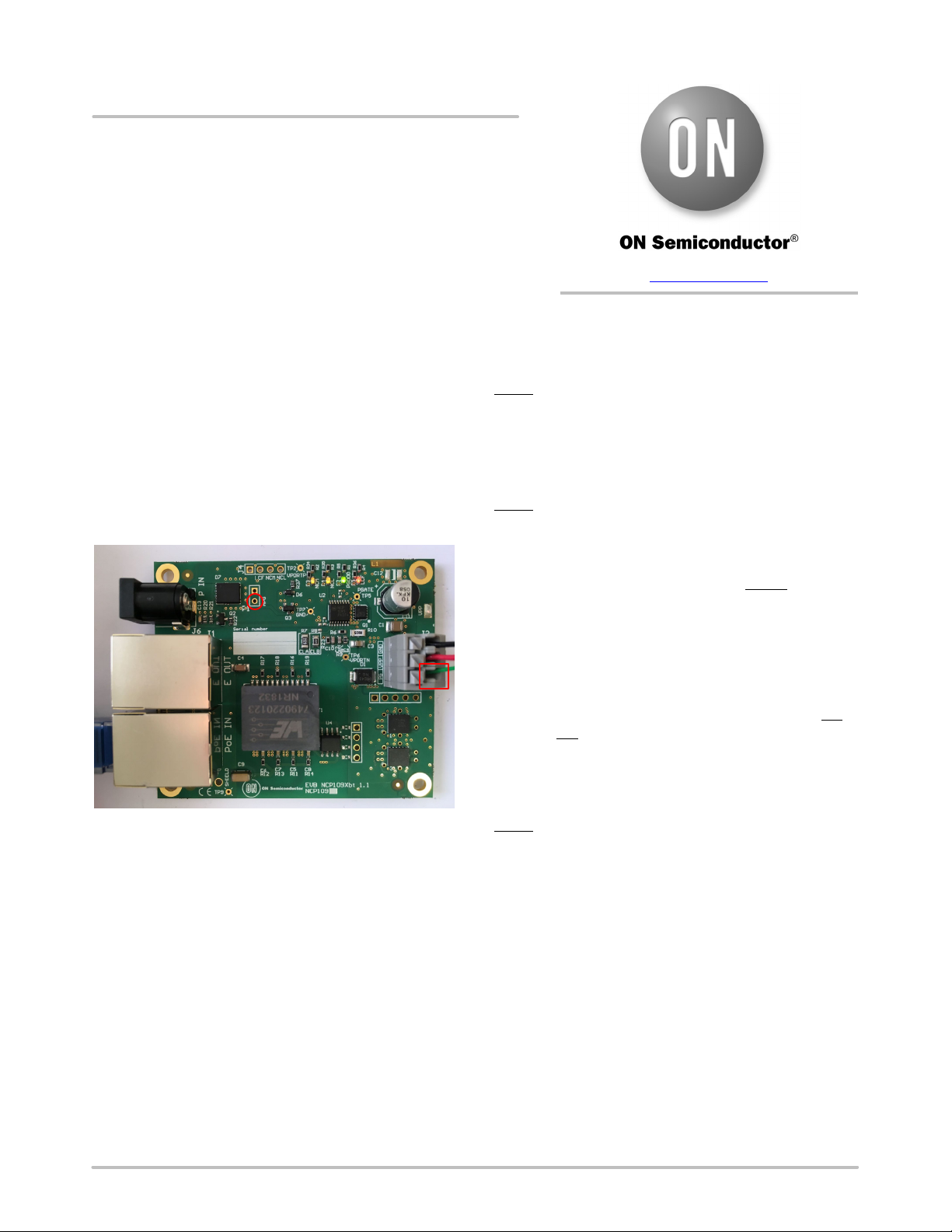
Figure 1. Operational NCP1095GEVB Showing
Basic Interconnections
The NCP1095GEVB board is designed as a PoE splitter:
having a PoE-enabled Ethernet port (labeled “PoE IN”) as
input and offering the power to a separate connector (J2)
while passing through the data to another Ethernet port
(labeled “E OUT”).
Quick Start Guide
Step 1: Connect the power connections available on
connector J2 (labeled “GND” and “VPP”) to the DC/DC
converter on the system that needs to be powered (cf. black
and red wires in the picture on the left). The DC/DC
converter behind the NCP1095 EVB should be operational
over a 34 V to 57 V voltage range.
Step 2
: Connect the control connection to the DC/DC
converter! It is important that the DC/DC converter or
any significant load is kept off when the pass-switch is
charging the input capacitance.
For a DC-DC converter with an undervoltage (UV or
UVLO) or an active high enable (EN or SHDN
signal on connector J2 could be used (cf. green wire in the
picture on the left). The “PG” signal will be clamped to 18 V
by a zener when the board is powered up. For some DC-DC
converter boards an additional diode in series with the
control connection might be required (cathode connected to
NCP1095 and anode connected to the DC-DC converter).
For a DC-DC converter with an active low enable (EN
SHDN or ON
The “nPG” signal will be pulled up to VPP during the inrush
phase. Always check the voltage rating of the enable,
shutdown or undervoltage pin of the DC-DC converter.
Step 3
on the left) coming from the PSE in the Ethernet connector
J3 labeled “PoE IN”.
If the PSE powers up the system the green PGOOD LED
should be ON.
The status of the remaining LEDs depends on the PSE
being used.
/OFF), the “nPG” signal on P1 could be used.
: Insert the Ethernet cable (cf. blue cable in the picture
), the “PG”
or
© Semiconductor Components Industries, LLC, 2019
June, 2019 − Rev. 0
1 Publication Order Number:
EVBUM2644/D
Page 2

NCP1095GEVB
Assigned Power
The NCP1095GEVB will request Class 8 during Physical
Layer classification. PDs need to take into account that they
can be underpowered and eventually be assigned to Class 3,
4 or 6.
The state of the NCM and NCL outputs provides
information about the power level that the PSE has assigned
to the NCP1095GEVB during classification. See Table 1 to
determine the assigned power based on the status of the
orange NCM and NCL leds.
Table 1. CLASSIFICATION RESULT
NCM
Led
off off 3 13 W
off on 4 25.5 W
on off 6 51 W
on on 8
NCL
Led
Assigned
Class
Assigned
Power
71.3…90 W
PDs assigned to Class 8 may consume greater than 71.3 W
as long as they guarantee not to exceed the 90 W power limit
at the PSE power interface. Operation beyond 71.3 W is,
however, only possible if additional information is available
to the PD regarding the actual link section DC resistance
between the PSE and the PD.
The application should always operate at or below the
assigned power limit. Failure to do so will result in the PSE
disconnecting the PD!
PSE Categorization
The state of the LCF output provides information
(retrieved during classification) about the type of PSE the
NCP1095GEVB is connected to. See Table 2 to determine
the PSE Type based on the status of the red LCF led.
System Startup
A PD can be underpowered and assigned to Class 3 only.
Therefore the DC/DC converter behind NCP1095GEVB
should not draw more than 13 W during start-up. Eventually
the soft-start setting of the DC/DC converter might need to
be adapted to accomplish this.
Requested Power
As mentioned before, the NCP1095GEVB will request
Class 8 during Physical Layer classification. If a lower Class
or power level is preferred, resistor R8 labeled “CLB”
and/or resistor R7 labeled “CLA” should be changed. See
the NCP1095 datasheet
for the nominal resistance values.
The Class the PD is actually assigned to is always limited
to the requested Class.
Autoclass
The NCP1095GEVB will by default not request
Autoclass during Physical Layer classification. If the PD
should request Autoclass, remove 0E resistor R9 labeled
“acs”.
Maintain Power Signature (MPS)
A PD should draw a minimum amount of current in order
to prevent the PSE from removing power. The load resistor
R15 was added on the bottom side of the board to make sure
the load current is always sufficient and the NCP1095GEVB
remains powered.
Depending on the minimum current the system may draw,
the resistance value of R15 should be increased for the final
design in order not to waste power unnecessarily.
For some systems, the load resistor can even be omitted.
Table 2. PSE TYPE
LCF Led PSE Categorization
off The PSE is categorized according to 802.3af/at
(PSE Type 1 or Type 2)
on The PSE is categorized according to 802.3bt
(PSE Type 3 or Type 4)
The PSE Type determines the MPS timing. It also
indicates to a PD requesting Autoclass whether it makes
sense to go to the maximum power state according to its
assigned Class.
www.onsemi.com
2
Page 3

NCP1095GEVB
Figure 2. Schematic Diagram NCP1095 EVB
www.onsemi.com
3
Page 4

NCP1095GEVB
Auxiliary Supply
The NCP1095GEVB supports drawing power from an
alternate or local power source in applications connected to
non-PoE enabled networks. A rear auxiliary supply can be
inserted in connector J6 labeled “P IN”.
The recommended voltage of the auxiliary supply is 24 V.
Table 3. ELECTRICAL CHARACTERISTICS
Operating Range
Auxiliary Input Voltage
Auxiliary Input Current
Auxiliary Input Voltage,
Extended [Warning!]
20−30 V
0–5 A
10–57 V
If an auxiliary supply that is too low (10.1 V … 20 V) is
inserted before the UVLO threshold was crossed by the PSE,
the class driver could become unintentionally activated.
Therefore it is recommended to adapt the AUX resistor
divider to R
= 33 kW and R23 = 15 kW for operation with
22
a low voltage auxiliary supply voltage.
The NCP1095GEVB is able to operate with an auxiliary
supply voltage up to 57 V. However the customer must take
caution when using a high voltage (>30 V) auxiliary supply:
the NCP1095GEVB has to be unpowered when this high
voltage (30 V … 57 V) supply is inserted.
Do not insert a high voltage (>30 V) auxiliary supply
when the NCP1095GEVB is already powered by a PSE.
Violating the warning above may result in the PD sourcing
power on the “PoE IN” Ethernet connector.
If the customer needs to implement a system in which
a high voltage (>30 V) rear auxiliary supply can be inserted
while the PD is already powered by the PSE, both
GreenBridge2 rectifiers (U1 and U3) need a gate drive
circuit allowing them to be disabled. Figure 4 shows a gate
drive circuit (GDC) able to turn off the GreenBridge2
internal top MOSFETs.
G3
BC846BPDW1
IN1 IN2
Figure 4. Basic GreenBridge2 GDC with disable
1.5M
G4
DF6A6.8FUT1G
NCP1095_GBR
BC846BPDW1
1.5M
½ BAV70LT1G
G2
G1
If the AUX input pin of NCP1095 is pulled high, it will
immediately drive the GBR pin low. The above gate drive
circuit controlled by the GBR pin makes sure the PD does
not source power under any circumstance in combination
with a high voltage (>30 V) auxiliary supply.
The gate drive circuit shown in Figure 4 is NOT
implemented on NCP1095GEVB. Therefore a high voltage
(>30 V) auxiliary supply should not be inserted when
NCP1095GEVB is already powered by a PSE.
G3 G2
G3
BC846BPDW1
162K
IN1 IN2
MMBZ27VALT1G
BC846BPDW1
G4 G1
Figure 3. Operational NCP1095GEVB Showing
Basic Interconnections
www.onsemi.com
4
Page 5

ON Semiconductor and the ON Semiconductor logo are trademarks of Semiconductor Components Industries, LLC dba ON Semiconductor or its subsidiaries in the United States and/or
other countries. ON Semiconductor owns the rights to a number of patents, trademarks, copyrights, trade secrets, and other intellectual property. A listing of ON Semiconductor’s
product/patent coverage may be accessed at www.onsemi.com/site/pdf/Patent−Marking.pdf. ON Semiconductor is an Equal Opportunity/Affirmative Action Employer. This literature is
subject to all applicable copyright laws and is not for resale in any manner.
The evaluation board/kit (research and development board/kit) (hereinafter the “board”) is not a finished product and is as such not available for sale to consumers. The board is only intended
for research, development, demonstration and evaluation purposes and should as such only be used in laboratory/development areas by persons with an engineering/technical training
and familiar with the risks associated with handling electrical/mechanical components, systems and subsystems. This person assumes full responsibility/liability for proper and safe handling.
Any other use, resale or redistribution for any other purpose is strictly prohibited.
The board is delivered “AS IS” and without warranty of any kind including, but not limited to, that the board is production−worthy, that the functions contained in the board will meet your
requirements, or that the operation of the board will be uninterrupted or error free. ON Semiconductor expressly disclaims all warranties, express, implied or otherwise, including without
limitation, warranties of fitness for a particular purpose and non−infringement of intellectual property rights.
ON Semiconductor reserves the right to make changes without further notice to any board.
You are responsible for determining whether the board will be suitable for your intended use or application or will achieve your intended results. Prior to using or distributing any systems
that have been evaluated, designed or tested using the board, you agree to test and validate your design to confirm the functionality for your application. Any technical, applications or design
information or advice, quality characterization, reliability data or other services provided by ON Semiconductor shall not constitute any representation or warranty by ON Semiconductor,
and no additional obligations or liabilities shall arise from ON Semiconductor having provided such information or services.
The boards are not designed, intended, or authorized for use in life support systems, or any FDA Class 3 medical devices or medical devices with a similar or equivalent classification in
a foreign jurisdiction, or any devices intended for implantation in the human body. Should you purchase or use the board for any such unintended or unauthorized application, you shall
indemnify and hold ON Semiconductor and its officers, employees, subsidiaries, affiliates, and distributors harmless against all claims, costs, damages, and expenses, and reasonable
attorney fees arising out of, directly or indirectly, any claim of personal injury or death associated with such unintended or unauthorized use, even if such claim alleges that ON Semiconductor
was negligent regarding the design or manufacture of the board.
This evaluation board/kit does not fall within the scope of the European Union directives regarding electromagnetic compatibility, restricted substances (RoHS), recycling (WEEE), FCC,
CE or UL, and may not meet the technical requirements of these or other related directives.
FCC WARNING – This evaluation board/kit is intended for use for engineering development, demonstration, or evaluation purposes only and is not considered by ON Semiconductor to
be a finished end product fit for general consumer use. It may generate, use, or radiate radio frequency energy and has not been tested for compliance with the limits of computing devices
pursuant to part 15 of FCC rules, which are designed to provide reasonable protection against radio frequency interference. Operation of this equipment may cause interference with radio
communications, in which case the user shall be responsible, at its expense, to take whatever measures may be required to correct this interference.
ON Semiconductor does not convey any license under its patent rights nor the rights of others.
LIMITATIONS OF LIABILITY: ON Semiconductor shall not be liable for any special, consequential, incidental, indirect or punitive damages, including, but not limited to the costs of
requalification, delay, loss of profits or goodwill, arising out of or in connection with the board, even if ON Semiconductor is advised of the possibility of such damages. In no event shall
ON Semiconductor’s aggregate liability from any obligation arising out of or in connection with the board, under any theory of liability, exceed the purchase price paid for the board, if any.
For more information and documentation, please visit www.onsemi.com
.
PUBLICATION ORDERING INFORMATION
LITERATURE FULFILLMENT:
Literature Distribution Center for ON Semiconductor
19521 E. 32nd Pkwy, Aurora, Colorado 80011 USA
Phone: 303−675−2175 or 800−344−3860 Toll Free USA/Canada
Fax: 303−675−2176 or 800−344−3867 Toll Free USA/Canada
Email: orderlit@onsemi.com
◊
N. American Technical Support: 800−282−9855 Toll Free
USA/Canada
Europe, Middle East and Africa Technical Support:
Phone: 421 33 790 2910
www.onsemi.com
ON Semiconductor Website: www.onsemi.com
Order Literature: http://www.onsemi.com/orderlit
For additional information, please contact your local
Sales Representative
1
 Loading...