

2N3055A (NPN),
S
MJ15015 (NPN),
MJ15016 (PNP)
MJ15015 and MJ15016 are Preferred Devices
Complementary Silicon
High−Power Transistors
These PowerBaset complementary transistors are designed for
high power audio, stepping motor and other linear applications. These
devices can also be used in power switching circuits such as relay or
solenoid drivers, dc−to−dc converters, inverters, or for inductive loads
requiring higher safe operating area than the 2N3055.
Features
• Current−Gain − Bandwidth−Product @ I
fT= 0.8 MHz (Min) − NPN
= 2.2 MHz (Min) − PNP
• Safe Operating Area − Rated to 60 V and 120 V, Respectively
• Pb−Free Packages are Available*
MAXIMUM RATINGS (Note 1)
Rating Symbol Value Unit
Collector−Emitter Voltage
MJ15015, MJ15016
Collector−Base Voltage
MJ15015, MJ15016
Collector−Emitter Voltage Base
Reversed Biased 2N3055A
MJ15015, MJ15016
Emitter−Base Voltage V
Collector Current − Continuous I
Base Current I
Total Device Dissipation @ TC = 25_C
Derate above 25_C 2N3055A
2N3055A
2N3055A
= 1.0 Adc
C
V
CEO
V
CBO
V
CEV
EBO
C
B
P
D
60
120
100
200
100
200
7.0 Vdc
15 Adc
7.0 Adc
115
0.65
Vdc
Vdc
Vdc
W/_C
W
http://onsemi.com
15 AMPERE
COMPLEMENTARY SILICON
POWER TRANSISTORS
60, 120 VOLTS − 115, 180 WATT
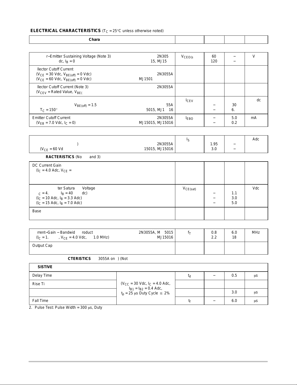
TO−204AA (TO−3)
CASE 1−07
STYLE 1
MARKING DIAGRAMS
2N3055AG
AYWW
MEX
MJ1501xG
AYWW
MEX
Total Device Dissipation @ TC = 25_C
Derate above 25_C
MJ15015, MJ15016
Operating and Storage Junction
Temperature Range
TJ, T
stg
180
1.03
−65 to +200
_C
THERMAL CHARACTERISTICS
Characteristics Symbol Max Max Unit
Thermal Resistance, Junction−to−Case
Stresses exceeding Maximum Ratings may damage the device. Maximum
Ratings are stress ratings only. Functional operation above the Recommended
Operating Conditions is not implied. Extended exposure to stresses above the
Recommended Operating Conditions may affect device reliability.
1. Indicates JEDEC Registered Data. (2N3055A)
*For additional information on our Pb−Free strategy and soldering details, please
download the ON Semiconductor Soldering and Mounting Techniques
Reference Manual, SOLDERRM/D.
© Semiconductor Components Industries, LLC, 2006
April, 2006 − Rev. 6
R
1.52 0.98
q
JC
_C/W
1 Publication Order Number:
2N3055A = Device Code
MJ1501x = Device Code
x = 5 or 6
G = Pb−Free Package
A = Assembly Location
Y = Year
WW = Work Week
MEX = Country of Origin
ORDERING INFORMATION
See detailed ordering and shipping information in the package
dimensions section on page 5 of this data sheet.
Preferred devices are recommended choices for future use
and best overall value.
2N3055A/D
2N3055A (NPN), MJ15015 (NPN), MJ15016 (PNP)
Î
Î
Î
Î
Î
Î
Î
Î
Î
Î
Î
Î
Î
Î
Î
Î
Î
Î
Î
Î
Î
Î
Î
Î
Î
Î
Î
Î
Î
Î
Î
Î
Î
Î
Î
Î
Î
Î
Î
Î
Î
Î
Î
Î
Î
Î
Î
Î
Î
Î
Î
Î
Î
Î
Î
Î
Î
Î
Î
Î
Î
Î
Î
Î
Î
Î
Î
Î
Î
Î
Î
Î
Î
Î
Î
ELECTRICAL CHARACTERISTICS (T
Characteristic
OFF CHARACTERISTICS (Note 2)
ООООООООООООООООООООООООООООООО
Collector−Emitter Sustaining Voltage (Note 3) 2N3055A
ООООООООООООООООООО
= 200 mAdc, IB = 0) MJ15015, MJ15016
(I
C
Collector Cutoff Current
ООООООООООООООООООО
(VCE = 30 Vdc, V
(VCE = 60 Vdc, V
ООООООООООООООООООО
Collector Cutoff Current (Note 3) 2N3055A
(V
= Rated Value, V
CEV
Collector Cutoff Current
ООООООООООООООООООО
(V
= Rated Value, V
CEV
TC = 150_C) MJ15015, MJ15016
ООООООООООООООООООО
Emitter Cutoff Current 2N3055A
(VEB = 7.0 Vdc, IC = 0) MJ15015, MJ15016
ООООООООООООООООООО
SECOND BREAKDOWN (Note 3)
ООООООООООООООООООООООООООООООО
Second Breakdown Collector Current with Base Forward Biased
(t = 0.5 s non−repetitive) 2N3055A
ООООООООООООООООООО
(VCE = 60 Vdc) MJ15015, MJ15016
= 0 Vdc) 2N3055A
BE(off)
= 0 Vdc) MJ15015, MJ15016
BE(off)
= 1.5 Vdc) MJ15015, MJ15016
BE(off)
= 1.5 Vdc, 2N3055A
BE(off)
= 25°C unless otherwise noted)
C
Symbol
V
CEO(sus)
ÎÎÎ
I
CEO
ÎÎÎ
ÎÎÎ
I
CEV
I
CEV
ÎÎÎ
ÎÎÎ
I
EBO
ÎÎÎ
I
S/b
ÎÎÎ
Min
60
ÎÎ
120
ÎÎ
−
−
ÎÎ
−
−
ÎÎ
−
−
ÎÎ
−
−
ÎÎ
1.95
ÎÎ
3.0
Max
−
Î
−
Î
0.7
0.1
Î
5.0
1.0
Î
30
6.0
Î
5.0
0.2
Î
−
Î
−
Unit
Vdc
ÎÎ
mAdc
ÎÎ
ÎÎ
mAdc
mAdc
ÎÎ
ÎÎ
mAdc
ÎÎ
Adc
ÎÎ
ON CHARACTERISTICS (Note 2 and 3)
DC Current Gain
(IC = 4.0 Adc, VCE = 2.0 Vdc)
ООООООООООООООООООО
(IC = 4.0 Adc, VCE = 4.0 Vdc)
ООООООООООООООООООО
(IC = 10 Adc, VCE = 4.0 Vdc)
h
FE
ÎÎÎ
ÎÎÎ
10
ÎÎ
20
ÎÎ
5.0
70
Î
70
Î
−
−
ÎÎ
ÎÎ
Collector−Emitter Saturation Voltage
ООООООООООООООООООО
(IC = 4.0 Adc, IB = 400 mAdc)
(IC = 10 Adc, IB = 3.3 Adc)
ООООООООООООООООООО
(IC = 15 Adc, IB = 7.0 Adc)
Base−Emitter On Voltage
ООООООООООООООООООО
(IC = 4.0 Adc, VCE = 4.0 Vdc)
DYNAMIC CHARACTERISTICS (Note 3)
Current−Gain − Bandwidth Product 2N3055A, MJ15015
(IC = 1.0 Adc, VCE = 4.0 Vdc, f = 1.0 MHz) MJ15016
ООООООООООООООООООО
Output Capacitance
(VCB = 10 Vdc, IE = 0, f = 1.0 MHz)
ООООООООООООООООООО
SWITCHING CHARACTERISTICS (2N3055A only) (Note 3)
RESISTIVE LOAD
Delay Time
ООООООО
Rise Time
Storage Time
Fall Time
(VCC = 30 Vdc, IC = 4.0 Adc,
IB1 = IB2 = 0.4 Adc,
ООООООО
tp = 25 ms Duty Cycle v 2%
ООООООО
2. Pulse Test: Pulse Width = 300 ms, Duty Cycle v 2%.
3. Indicates JEDEC Registered Data. (2N3055A)
V
CE(sat)
ÎÎÎ
ÎÎÎ
V
BE(on)
ÎÎÎ
f
T
ÎÎÎ
C
ob
ÎÎÎ
t
d
t
r
t
s
t
f
ÎÎ
−
−
ÎÎ
−
0.7
ÎÎ
0.8
2.2
ÎÎ
60
ÎÎ
−
−
−
−
Î
1.1
3.0
Î
5.0
1.8
Î
6.0
18
Î
600
Î
0.5
4.0
3.0
6.0
Vdc
ÎÎ
ÎÎ
Vdc
ÎÎ
MHz
ÎÎ
pF
ÎÎ
ms
ms
ms
ms
http://onsemi.com
2

2N3055A (NPN), MJ15015 (NPN), MJ15016 (PNP)
)
200
150
MJ15015
MJ15016
100
, DC CURRENT GAIN
FE
h
200
100
50
D(AV)
P , AVERAGE POWER DISSIPATION (W)
0
0 25 50 75 100 125 150 175 200
2N3055A
TC, CASE TEMPERATURE (°C)
Figure 1. Power Derating
2.8
TJ = 150°C
70
50
30
20
10
7
5
3
2
0.2
VCE = 4.0 V
0.3 0.5 0.7 1 2 3 5 7 15
−55 °C
25°C
10
IC, COLLECTOR CURRENT (AMP)
Figure 2. DC Current Gain
, COLLECTOR−EMITTER VOLTAGE (VOLTS
V
CE
2.4
2
1.6
1.2
0.8
0.4
IC = 1 A
0
0.005
0.01 0.02 0.05 0.1 0.2 0.5 1 2 5
IB, BASE CURRENT (AMP)
4 A
Figure 3. Collector Saturation Region
TJ = 25°C
8 A
V, VOLTAGE (VOLTS)
3.5
3
2.5
2
1.5
1
0.5
0
TC = 25°C
V
@ IC/IB = 10
BE(sat)
V
@ VCE = 4 V
BE(on)
V
@ IC/IB = 10
CE(sat)
0.2
0.3 0.5 0.7 1 2 3 5 7 20
IC, COLLECTOR CURRENT (AMP)
Figure 4. “On” Voltages
10
T
f, CURRENT−GAIN BANDWIDTH PRODUCT (MHz)
http://onsemi.com
3
10
5.0
2.0
1.0
0.1
MJ15016
2N3055A
MJ15015
0.2 0.3 0.5 1.0 2.0
IC, COLLECTOR CURRENT (AMPS)
Figure 5. Current−Gain — Bandwidth Product

25 ms
+13 V
0
−11 V
tr, tf ≤ 10 ns
DUTY CYCLE = 1.0%
2N3055A (NPN), MJ15015 (NPN), MJ15016 (PNP)
10
7
VCC = 30 V
5
V
CC
+30 V
7.5 W
30
SCOPE
W
1N6073
−5 V
IC/IB = 10
TJ = 25°C
3
2
t
r
1
0.7
t, TIME (s)μ
0.5
0.3
0.2
0.1
0.2
0.3 0.5 0.7 1 2 3 7 15
t
d
IC, COLLECTOR CURRENT (AMP)
510
Figure 6. Switching Times Test Circuit
Figure 7. Turn−On Time
(Circuit shown is for NPN)
10
7
5
3
2
t
0.1
t, TIME (s)μ
0.7
0.5
f
VCC = 30
t
s
IC/IB = 10
0.3
0.2
0.1
IB1 = IB2
TJ = 25°C
0.2
0.3 0.5 0.7 1 3 5 15
2
710
IC, COLLECTOR CURRENT (AMPS)
Figure 8. Turn−Off Times
C, CAPACITANCE (pF)
400
200
100
TJ = 25°C
2N3055A
C
ib
50
MJ15015
MJ15016
C
ob
30
20
1.0
20 50 100 200 500 10002.0 5.0 10
VR, REVERSE VOLTAGE (VOLTS)
Figure 9. Capacitances
http://onsemi.com
4

2N3055A (NPN), MJ15015 (NPN), MJ15016 (PNP)
NPN
PNP
COLLECTOR CUT−OFF REGION
10,000
1000
100
10
1.0
, COLLECTOR CURRENT (A)μI
C
0.1
0.01
20
10
5
2
, COLLECTOR CURRENT (AMPS)
C
I
1
VCE = 30 V
TJ = 150°C
100°C
IC = I
CES
REVERSE
25°C
+0.2
+0.1 0 −0.1 −0.2 −0.3 −0.4 −0.5
VBE, BASE−EMITTER VOLTAGE (VOLTS)
FORWARD
Figure 10. 2N3055A, MJ15015
BONDING WIRE LIMIT
THERMAL LIMIT @ TC = 25°C
(SINGLE PULSE)
SECOND BREAKDOWN LIMIT
10 20 10060
VCE, COLLECTOR−EMITTER VOLTAGE (VOLTS)
Figure 12. Forward Bias Safe Operating Area
2N3055A
30 ms
100 ms
1 ms
100 ms
dc
1000
, COLLECTOR CURRENT (A)μI
C
0.001
100
1.0
0.1
0.01
VCE = 30 V
10
TJ = 150°C
100°C
REVERSE FORWARD
25°C
−0.2
−0.1 0 +0.1 +0.2 +0.3
VBE, BASE−EMITTER VOLTAGE (VOLTS)
Figure 11. MJ15016
20
10
5.0
2.0
1.0
, COLLECTOR CURRENT (AMP)
0.5
C
I
0.2
15 20 10060
BONDING WIRE LIMIT
THERMAL LIMIT @ TC = 25°C
(SINGLE PULSE)
SECOND BREAKDOWN LIMIT
30 120
VCE, COLLECTOR−EMITTER VOLTAGE (VOLTS)
Figure 13. Forward Bias Safe Operating Area
MJ15015, MJ15016
IC = I
CES
+0.4 +0.5
0.1ms
1.0ms
100ms
dc
There are two limitations on the power handling ability of
a transistor: average junction temperature and second
breakdown. Safe Operating area curves indicate IC − V
CE
limits of the transistor that must be observed for reliable
operation; i.e., the transistor must not be subjected to greater
dissipation than the curves indicate.
ORDERING INFORMATION
Device Package Shipping
2N3055A TO−204
2N3055AG TO−204
MJ15015 TO−204
MJ15015G TO−204
MJ15016 TO−204
MJ15016G TO−204
(Pb−Free)
(Pb−Free)
(Pb−Free)
http://onsemi.com
5
The data of Figures 12 and 13 is based on TC = 25_C;
T
is variable depending on power level. Second
J(pk)
breakdown pulse limits are valid for duty cycles to 10% but
must be derated for temperature according to Figure 1.
100 Units / Tray
100 Units / Tray

2N3055A (NPN), MJ15015 (NPN), MJ15016 (PNP)
PACKAGE DIMENSIONS
TO−204 (TO−3)
CASE 1−07
ISSUE Z
A
N
C
E
2 PLD
0.13 (0.005) Y
U
V
H
L
2
1
G
−T−
K
M
−Y−
B
T
SEATING
PLANE
M
Q
M
−Q−
0.13 (0.005) T
M
M
Y
NOTES:
1. DIMENSIONING AND TOLERANCING PER ANSI
Y14.5M, 1982.
2. CONTROLLING DIMENSION: INCH.
3. ALL RULES AND NOTES ASSOCIATED WITH
REFERENCED TO−204AA OUTLINE SHALL APPLY.
DIM MIN MAX MIN MAX
A 1.550 REF 39.37 REF
B −−− 1.050 −−− 26.67
C 0.250 0.335 6.35 8.51
D 0.038 0.043 0.97 1.09
E 0.055 0.070 1.40 1.77
G 0.430 BSC 10.92 BSC
H 0.215 BSC 5.46 BSC
K 0.440 0.480 11.18 12.19
L 0.665 BSC 16.89 BSC
N −−− 0.830 −−− 21.08
Q 0.151 0.165 3.84 4.19
U 1.187 BSC 30.15 BSC
V 0.131 0.188 3.33 4.77
STYLE 1:
PIN 1. BASE
2. EMITTER
CASE: COLLECTOR
MILLIMETERSINCHES
PowerBase is a trademark of Semiconductor Components Industries, LLC.
ON Semiconductor and are registered trademarks of Semiconductor Components Industries, LLC (SCILLC). SCILLC reserves the right to make changes without further notice
to any products herein. SCILLC makes no warranty, representation or guarantee regarding the suitability of its products for any particular purpose, nor does SCILLC assume any liability
arising out of the application or use of any product or circuit, and specifically disclaims any and all liability, including without limitation special, consequential or incidental damages.
“Typical” parameters which may be provided in SCILLC data sheets and/or specifications can and do vary in different applications and actual performance may vary over time. All
operating parameters, including “Typicals” must be validated for each customer application by customer’s technical experts. SCILLC does not convey any license under its patent rights
nor the rights of others. SCILLC products are not designed, intended, or authorized for use as components in systems intended for surgical implant into the body, or other applications
intended to support or sustain life, or for any other application in which the failure of the SCILLC product could create a situation where personal injury or death may occur. Should
Buyer purchase or use SCILLC products for any such unintended or unauthorized application, Buyer shall indemnify and hold SCILLC and its officers, employees, subsidiaries, affiliates,
and distributors harmless against all claims, costs, damages, and expenses, and reasonable attorney fees arising out of, directly or indirectly, any claim of personal injury or death
associated with such unintended or unauthorized use, even if such claim alleges that SCILLC was negligent regarding the design or manufacture of the part. SCILLC is an Equal
Opportunity/Affirmative Action Employer. This literature is subject to all applicable copyright laws and is not for resale in any manner.
PUBLICATION ORDERING INFORMATION
LITERATURE FULFILLMENT:
Literature Distribution Center for ON Semiconductor
P.O. Box 61312, Phoenix, Arizona 85082−1312 USA
Phone: 480−829−7710 or 800−344−3860 Toll Free USA/Canada
Fax: 480−829−7709 or 800−344−3867 Toll Free USA/Canada
Email: orderlit@onsemi.com
N. American Technical Support: 800−282−9855 Toll Free
USA/Canada
Japan: ON Semiconductor, Japan Customer Focus Center
2−9−1 Kamimeguro, Meguro−ku, Tokyo, Japan 153−0051
Phone: 81−3−5773−3850
http://onsemi.com
ON Semiconductor Website: http://onsemi.com
Order Literature: http://www.onsemi.com/litorder
For additional information, please contact your
local Sales Representative.
2N3055A/D
6
 Loading...