

Page 1
查询MCR218FP-6FP供应商
MDC3105
Integrated Relay,
Inductive Load Driver
This device is intended to replace an array of three to six discrete
components with an integrated SMT part. It is available in a SOT−23
package. It can be used to switch 3 to 6 Vdc inductive loads such as
relays, solenoids, incandescent lamps, and small DC motors without
the need of a free−wheeling diode.
Features
• Provides a Robust Driver Interface between DC Relay Coil and
Sensitive Logic Circuits
• Optimized to Switch Relays from a 3.0 V to 5.0 V Rail
• Capable of Driving Relay Coils Rated up to 2.5 W at 5.0 V
• Features Low Input Drive Current and Good Back−to−Front Transient
Isolation
• Internal Zener Eliminates Need for Free−Wheeling Diode
• Internal Zener Clamp Routes Induced Current to Ground for Quieter
System Operation
• Guaranteed Off State with No Input Connection
• Supports Large Systems with Minimal Off−State Leakage
• ESD Resistant in Accordance with the Class 1C Human Body Model
• Low Sat Voltage Reduces System Current Drain by Allowing Use of
Higher Resistance Relay Coils
• Pb−Free Packages are Available
Applications
• Telecom: Line Cards, Modems, Answering Machines, FAX
Machines, Feature Phone Electronic Hook Switch
• Computer and Office: Photocopiers, Printers, Desktop Computers
• Consumer: TVs and VCRs, Stereo Receivers, CD Players, Cassette
Recorders, TV Set Top Boxes
• Industrial: Small Appliances, White Goods, Security Systems,
Automated Test Equipment, Garage Door Openers
• Automotive: 5.0 V Driven Relays, Motor Controls, Power Latches,
Lamp Drivers
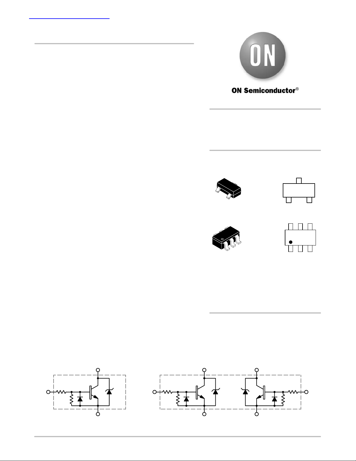
http://onsemi.com
Relay, Inductive Load Driver
Silicon SMALLBLOCKt
Integrated Circuit
MARKING
DIAGRAMS
SOT−23
1
1
JW = Specific Device Code
M = Date Code*
G = Pb−Free Package
(Note: Microdot may be in either location)
*Date Code orientation and/or overbar may
vary depending upon manufacturing location.
ORDERING INFORMATION
See detailed ordering and shipping information in the package
dimensions section on page 2 of this data sheet.
CASE 318
STYLE 6
SC−74
CASE 318F
STYLE 8
JW M G
G
1
JW M G
G
1
INTERNAL CIRCUIT DIAGRAMS
V
(3)
out
V
1.0 k
in
(1)
33 k
GND (2)
© Semiconductor Components Industries, LLC, 2005
December, 2005 − Rev. 5
6.6 V
V
(6)
out
V
1.0 k
(5)
in
33 k
GND (1)
1 Publication Order Number:
6.6 V
CASE 318FCASE 318
6.6 V
V
out
GND (4)
(3)
1.0 k
33 k
MDC3105/D
(2)
V
in
Page 2
MDC3105
MAXIMUM RATINGS (T
= 25°C unless otherwise noted)
J
Rating Symbol Value Unit
Power Supply Voltage V
Input Voltage V
Reverse Input Voltage V
CC
in(fwd)
in(rev)
6.0 Vdc
6.0 Vdc
−0.5 Vdc
Repetitive Pulse Zener Energy Limit (Duty Cycle ≤ 0.01%) SOT−23 Ezpk 50 mJ
Output Sink Current − Continuous I
Junction Temperature T
Operating Ambient Temperature Range T
Storage Temperature Range T
O
J
A
stg
500 mA
150 °C
− 40 to +85 °C
− 65 to +150 °C
Maximum ratings are those values beyond which device damage can occur. Maximum ratings applied to the device are individual stress limit
values (not normal operating conditions) and are not valid simultaneously. If these limits are exceeded, device functional operation is not implied,
damage may occur and reliability may be affected.
THERMAL CHARACTERISTICS
Rating Symbol Value Unit
Total Device Power Dissipation (Note 1) SOT−23
Derate above 25°C
Total Device Power Dissipation (Note 1) SC−74
Derate above 25°C
Thermal Resistance Junction−to−Ambient SOT−23
SC−74
1. FR−5 PCB of 1″ x 0.75″ x 0.062″, TA = 25°C
P
D
P
D
R
q
JA
225
1.8
380
1.5
556
329
mW
mW/°C
mW
mW/°C
°C/W
ELECTRICAL CHARACTERISTICS (T
= 25°C unless otherwise noted)
A
Characteristic Symbol Min Typ Max Unit
OFF CHARACTERISTICS
Output Zener Breakdown Voltage
(@ IT = 10 mA Pulse)
Output Leakage Current @ 0 Input Voltage
(VO = 5.5 Vdc, Vin = O.C., TA = 25°C)
(VO = 5.5 Vdc, Vin = O.C., TA = 85°C)
Guaranteed “OFF” State Input Voltage (IO ≤ 100 mA)
V
(BRout)
V
(−BRout)
I
OO
V
in(off)
6.2−6.6
−
−
−0.7
−−0.1
7.0
−
30
− − 0.4 V
V
V
mA
ON CHARACTERISTICS
Input Bias Current (HFE Limited)
(IO = 250 mA, VO = 0.25 Vdc)
Output Saturation Voltage
(IO = 250 mA, Iin = 1.5 mA)
Output Sink Current − Continuous
(VCE = 0.25 Vdc, Iin = 1.5 mA)
V
I
I
in
O(sat)
O(on)
− 0.8 1.6
mAdc
Vdc
− 0.12 0.16
mA
250 400 −
ORDERING INFORMATION
Device Package Shipping
MDC3105LT1 SOT−23
MDC3105LT1G SOT−23
(Pb−Free)
MDC3105DMT1 SC−74
3000 / Tape & Reel
MDC3105DMT1G SC−74
(Pb−Free)
†For information on tape and reel specifications, including part orientation and tape sizes, please refer to our Tape and Reel Packaging
Specifications Brochure, BRD8011/D.
†
http://onsemi.com
2
Page 3
TYPICAL APPLICATION−DEPENDENT SWITCHING PERFORMANCE
SWITCHING CHARACTERISTICS
Characteristic Symbol Min Typ Max Units
Propagation Delay Times:
Transition Times:
High to Low Propagation Delay; Figure 1 (5.0 V 74HC04)
Low to High Propagation Delay; Figure 1 (5.0 V 74HC04)
High to Low Propagation Delay; Figures 1, 13 (3.0 V 74HC04)
Low to High Propagation Delay; Figures 1, 13 (3.0 V 74HC04)
High to Low Propagation Delay; Figures 1, 14 (5.0 V 74LS04)
Low to High Propagation Delay; Figures 1, 14 (5.0 V 74LS04)
Fall Time; Figure 1 (5.0 V 74HC04)
Rise Time; Figure 1 (5.0 V 74HC04)
Fall Time; Figures 1, 13 (3.0 V 74HC04)
Rise Time; Figures 1, 13 (3.0 V 74HC04)
Fall Time; Figures 1, 14 (5.0 V 74LS04)
Rise Time; Figures 1, 14 (5.0 V 74LS04)
V
in
V
out
50%
MDC3105
t
PLH
90%
50%
10%
t
r
Figure 1. Switching Waveforms
t
f
t
PHL
t
PHL
t
PLH
t
PHL
t
PLH
t
PHL
t
PLH
−
55
85
55
−
−
−
−
−
−
mS
−
430
−
−
315
−
−
2.4
nS
nS
t
f
t
r
t
f
t
r
t
f
t
r
−
45
70
45
−
−
−
−
−
−
mS
−
160
−
−
195
−
−
2.4
V
CC
GND
V
Z
V
CC
GND
http://onsemi.com
3
Page 4
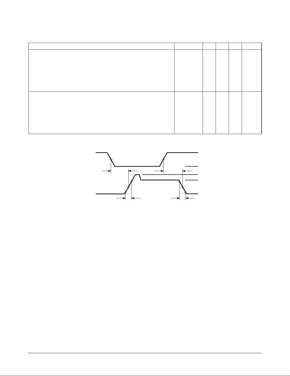
TYPICAL PERFORMANCE CHARACTERISTICS
out/Iin
, TRANSISTOR DC CURRENT GAIN
FE
H
500
450
400
350
300
250
200
150
100
MDC3105
(ON CHARACTERISTICS)
5.0
INPUT VOLTAGE (VOLTS)
4.5
4.0
3.5
3.0
2.5
2.0
1.5
1.0
0.5
MC68HC05C8
@ 5.0 Vdc
MC54LS04
+BAL99LT1
0
INPUT CURRENT (mA)
TJ = 85°C
25°C
−40°C
VO = 1.0 V
50
0
10 3.0 3.50.5 1.0 1.5 2.0
IO, OUTPUT SINK CURRENT (mA)
VO = 0.25 V
100 10001.0
Figure 2. Transistor DC Current Gain Figure 3. Input V−I Requirement Compared to
Possible Source Logic Outputs
MC74HC04
@ 4.5 Vdc
MDC3105LT1
Vin vs. I
MC68HC05C8 @ 3.3 Vdc
MC14049B @ 4.5 Vdc
2.5 4.00
in
MC74HC04
@ 3.0 Vdc
TJ = 25°C
VO = 0.25 V
OUTPUT CURRENT (mA)
, OUTPUT VOLTAGE (Vdc)V
out
50
45
40
35
30
25
20
15
10
5.0
0
0
0.01 0.02 0.03 0.04 0.05 0.5 3.01.5 4.0 4.5 5.0
INPUT CURRENT (mA)
TJ = 85°C
25°C
−40 °C
0.06 0.07 0.08 0.09 0.1
, OUTPUT CURRENT (mA)
out
I
500
400
300
200
100
Iin = 1.5 mA
1.2 mA
1.0 mA
0.8 mA
0.6 mA
0.4 mA
0
1.00
2.0
VO, OUTPUT VOLTAGE (Vdc)
2.5 3.5
Figure 4. Threshold Effects Figure 5. Transistor Output V−I Characteristic
1.3
1.2
1.1
1.0
0.9
0.8
0.7
0.6
0.5
0.4
0.3
0.2
0.1
0
10 mA
0.10.04
50 mA
Iin, INPUT CURRENT (mA)
125 mA
175 mA
1.0 10 1000
Figure 6. Output Saturation Voltage versus
I
TJ = 25°C
TJ = −40°C
I
out
500 mA
350 mA
=
8.5
8.0
7.5
7.0
6.5
, ZENER CLAMP VOLTAGE (VOLTS)
Z
V
6.0
1.0 100
TJ = 85°C
25°C
−40 °C
10
IZ, ZENER CURRENT (mA)
Figure 7. Zener Clamp Voltage versus Zener
Current
0.2 mA
0.1 mA
http://onsemi.com
4
Page 5

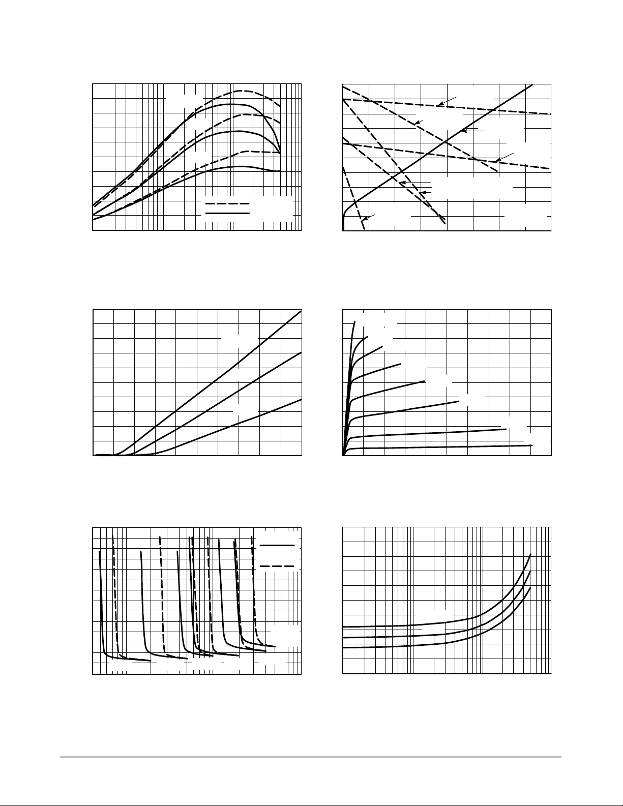
MDC3105
TYPICAL PERFORMANCE CHARACTERISTICS
(OFF CHARACTERISTICS)
10,000 k
VCC = 5.5 Vdc
1000 k
100 k
10 k
1.0 k
100
OUTPUT LEAKAGE CURRENT (nA)
10
1.0
−55 −35 25 85
−15 5.0 6545
TJ, JUNCTION TEMPERATURE (°C)
Vin = 0.5 Vdc
Vin = 0.35 Vdc
Figure 8. Output Leakage Current versus
Temperature
1.0
R
CE(sat)
Vin = 0 Vdc
100 k
10 k
1.0 k
OUTPUT LEAKAGE CURRENT (nA)
TJ = 25°C
100
10
1.0
0
0 1.0 2.0 3.0
Figure 9. Output Leakage Current versus
I
= 500 mA
out(max)
°PW = 10 ms
DC = 20%
Vin = 0.5 Vdc
Vin = 0.35 Vdc
Vin = 0 Vdc
4.0 5.0 6.0 7.0
VCC, SUPPLY VOLTAGE (Vdc)
Supply Voltage
°PW = 7.0 ms
DC = 5%
*24 ms
*34 ms
TA = 25°C
° = TRANSISTOR PC THERMAL LIMIT
* = MAX L/R FROM ZENER PULSED ENERGY LIMIT
(REFER TO FIGURE 11)
0.1
0.01
0.1
°CONTINUOUS DUTY
1.0 10
V
(VOLTS)
out
Figure 10. Safe Operating Area for MDC3105LT1
°PW = 0.1 s
DC = 50%
V
CC(max)
= +6.0 Vdc
*90 ms
*232 ms
*375 ms
TYPICAL
IZ vs V
Z
http://onsemi.com
5
Page 6

100 k
10 k
1.0 k
MAX L/R TIME CONSTANT (ms)
100
MDC3105
TA = 25°C
E
= 50 mJ
max
L/R = 2 * E
÷ (Vzpk * Izpk)
max
10
0.001
1.0
D = 0.5
0.1
0.01
r(t), TRANSIENT THERMAL
RESISTANCE (NORMALIZED)
0.001
0.01 0.1 1.0 10 100 1000 10,000 100,000 1,000,000
0.2
0.1
0.05
0.02
0.01
SINGLE PULSE
0.01 1.0
0.1
Izpk (AMPS)
Figure 11. Zener Repetitive Pulse Energy Limit
on L/R Time Constant for MDC3105LT1
P
d(pk)
t
PW
DUTY CYCLE = t1/t
t1, PULSE WIDTH (ms)
Figure 12. Transient Thermal Response for MDC3105LT1
1
t
PERIOD
2
2
http://onsemi.com
6
Page 7

MDC3105
Using TTR Designing for Pulsed Operation
For a repetitive pulse operating condition, time averaging
allows one to increase a device’s peak power dissipation
rating above the average rating by dividing by the duty cycle
of the repetitive pulse train. Thus, a continuous rating of 200
mW of dissipation is increased to 1.0 W peak for a 20% duty
cycle pulse train. However, this only holds true for pulse
widths which are short compared to the thermal time
constant of the semiconductor device to which they are
applied.
For pulse widths which are significant compared to the
thermal time constant of the device, the peak operating
condition begins to look more like a continuous duty
operating condition over the time duration of the pulse. In
these cases, the peak power dissipation rating cannot be
merely time averaged by dividing the continuous power
rating by the duty cycle of the pulse train. Instead, the
average power rating can only be scaled up a reduced
amount in accordance with the device’s transient thermal
response, so that the device’s max junction temperature is
not exceeded.
Figure 12 of the MDC3105 data sheet plots its transient
thermal resistance, r(t) as a function of pulse width in ms for
various pulse train duty cycles as well as for a single pulse
and illustrates this effect. For short pulse widths near the left
side of the chart, r(t), the factor, by which the continuous
duty thermal resistance is multiplied to determine how much
the peak power rating can be increased above the average
power rating, approaches the duty cycle of the pulse train,
which is the expected value. However, as the pulse width is
increased, that factor eventually approaches 1.0 for all duty
cycles indicating that the pulse width is sufficiently long to
appear as a continuous duty condition to this device. For the
MDC3105LT1, this pulse width is about 100 seconds. At
this and larger pulse widths, the peak power dissipation
capability is the same as the continuous duty power
capability.
To use Figure 12 to determine the peak power rating for
a specific application, enter the chart with the worst case
pulse condition, that is the max pulse width and max duty
cycle and determine the worst case r(t) for your application.
Then calculate the peak power dissipation allowed by using
the equation,
Pd(pk) = (T
Pd(pk) = (150°C
Jmax
− T
− T
) ÷ (R
Amax
) ÷ (556°C/W * r(t))
Amax
q
JA
* r(t))
Thus for a 20% duty cycle and a PW = 40 ms, Figure 12
yields r(t) = 0.3 and when entered in the above equation, the
max allowable Pd(pk) = 390 mW for a max TA = 85°C.
Also note that these calculations assume a rectangular
pulse shape for which the rise and fall times are insignificant
compared to the pulse width. If this is not the case in a
specific application, then the VO and IO waveforms should
be multiplied together and the resulting power waveform
integrated to find the total dissipation across the device. This
then would be the number that has to be less than or equal to
the Pd(pk) calculated above. A circuit simulator having a
waveform calculator may prove very useful for this purpose.
Notes on SOA and Time Constant Limitations
Figure 10 is the Safe Operating Area (SOA) for the
MDC3105. Device instantaneous operation should never be
pushed beyond these limits. It shows the SOA for the
Transistor “ON” condition as well as the SOA for the Zener
during the turn−off transient. The max current is limited by
the Izpk capability of the Zener as well as the transistor in
addition to the max input current through the resistor. It
should not be exceeded at any temperature. The BJT power
dissipation limits are shown for various pulse widths and
duty cycles at an ambient temperature of 25°C. The voltage
limit is the max VCC that can be applied to the device. When
the input to the device is switched off, the BJT “ON” current
is instantaneously dumped into the Zener diode where it
begins its exponential decay. The Zener clamp voltage is a
function of that BJT current level as can be seen by the
bowing of the VZ versus IZ curve at the higher currents. In
addition to the Zener’s current limit impacting this device’s
500 mA max rating, the clamping diode also has a peak
energy limit as well. This energy limit was measured using
a rectangular pulse and then translated to an exponential
equivalent using the 2:1 relationship between the L/R time
constant of an exponential pulse and the pulse width of a
rectangular pulse having equal energy content. These L/R
time constant limits in ms appear along the VZ versus I
curve for the various values of IZ at which the Pd lines
intersect the VCC limit. The L/R time constant for a given
load should not exceed these limits at their respective
currents. Precise L/R limits on Zener energy at intermediate
current levels can be obtained from Figure 11.
Z
http://onsemi.com
7
Page 8

MDC3105
APPLICATIONS DIAGRAMS
Designing with this Data Sheet
1. Determine the maximum inductive load current (at
max VCC, min coil resistance and usually minimum
temperature) that the MDC3105 will have to drive
and make sure it is less than the max rated current.
2. For pulsed operation, use the Transient Thermal
Response of Figure 12 and the instructions with it
to determine the maximum limit on transistor power
dissipation for the desired duty cycle and
temperature range.
3. Use Figures 10 and 11 with the SOA notes above to
insure that instantaneous operation does not push
the device beyond the limits of the SOA plot.
4. While keeping any V
requirements in mind,
O(sat)
determine the max input current needed to achieve
that output current from Figures 2 and 6.
5. For levels of input current below 100 mA, use the
input threshold curves of Figure 4 to verify that
+3.0 ≤ VDD ≤ +3.75 Vdc
+4.5 ≤ VCC ≤ +5.5 Vdc
there will be adequate input current available to turn
on the MDC3105 at all temperatures.
6. For levels of input current above 100 mA, enter
Figure 3 using that max input current and determine
the input voltage required to drive the MDC3105
from the solid Vin versus Iin line. Select a suitable
drive source family from those whose dotted lines
cross the solid input characteristic line to the right
of the Iin, Vin point.
7. Using the max output current calculated in step 1,
check Figure 7 to insure that the range of Zener
clamp voltage over temperature will satisfy all
system and EMI requirements.
8. Using Figures 8 and 9, insure that “OFF” state
leakage over temperature and voltage extremes does
not violate any system requirements.
9. Review circuit operation and insure none of the
device max ratings are being exceeded.
74HC04 OR
EQUIVALENT
+
+
AROMAT
TX2−L2−5 V
V
(6)
out
MDC3105DMT1
Vin (5)
GND (1)
Figure 13. A 200 mW, 5.0 V Dual Coil Latching Relay Application
with 3.0 V−HCMOS Level Translating Interface
V
(3)
out
GND (4)
Vin (2)
74HC04 OR
EQUIVALENT
http://onsemi.com
8
Page 9

Max Continuous Current Calculation
for TX2−5V Relay, R1 = 178 W Nominal @ RA = 25°C
Assuming ±10% Make Tolerance,
R1 = 178 W * 0.9 = 160 W Min @ TA = 25°C
TC for Annealed Copper Wire is 0.4%/°C
R1 = 160 W * [1+(0.004) * (−40°−25°)] = 118 W Min @ −40°C
IO Max = (5.5 V Max − 0.25V) /118 W = 45 mA
+4.5 TO +5.5 Vdc
+
AROMAT
TX2−5V
−
V
(3)
out
MDC3105LT1
74LS04
BAL99LT1
MDC3105
+4.5 TO +5.5 Vdc
EQUIVALENT
74HC04 OR
−
AROMAT
JS1E−5V
+
+
AROMAT
JS1E−5V
−
V
MDC3105LT1
out
−
AROMAT
JS1E−5V
+
+
AROMAT
JS1E−5V
−
(3)
Vin (1)
GND (2)
Figure 14. A 140 mW, 5.0 V Relay with TTL Interface
Figure 15. A Quad 5.0 V, 360 mW Coil Relay Bank
http://onsemi.com
9
Page 10

MDC3105
TYPICAL OPERATING WAVEFORMS
(VOLTS)
in
V
4.5
3.5
2.5
1.5
500
M
10 30 50 70 90
TIME (ms)
Figure 16. 20 Hz Square Wave Input
9
7
(mA)
C
I
225
175
125
75
25
10 30 50 70 90
TIME (ms)
Figure 17. 20 Hz Square Wave Response
172
132
(VOLTS)
out
V
5
3
1
10 30 50 70 90
TIME (ms)
Figure 18. 20 Hz Square Wave Response
(mA)
Z
I
92
52
12
10 30 50 70 90
TIME (ms)
Figure 19. 20 Hz Square Wave Response
http://onsemi.com
10
Page 11

MDC3105
PACKAGE DIMENSIONS
SOT−23 (TO−236)
CASE 318−08
ISSUE AN
D
3
E
12
b
e
SEE VIEW C
H
E
c
0.25
q
A
L
A1
L1
VIEW C
NOTES:
1. DIMENSIONING AND TOLERANCING PER ANSI
Y14.5M, 1982.
2. CONTROLLING DIMENSION: INCH.
3. MAXIMUM LEAD THICKNESS INCLUDES LEAD
FINISH THICKNESS. MINIMUM LEAD
THICKNESS IS THE MINIMUM THICKNESS OF
BASE MATERIAL.
4. 318−01 THRU −07 AND −09 OBSOLETE, NEW
STANDARD 318−08.
DIMAMIN NOM MAX MIN
A1 0.01 0.06 0.10 0.001
b 0.37 0.44 0.50 0.015
c 0.09 0.13 0.18 0.003
D 2.80 2.90 3.04 0.110
E 1.20 1.30 1.40 0.047
e 1.78 1.90 2.04 0.070
L 0.10 0.20 0.30 0.004
L1
H
E
STYLE 6:
PIN 1. BASE
MILLIMETERS
0.89 1.00 1.11 0.035
0.35 0.54 0.69 0.014 0.021 0.029
2.10 2.40 2.64 0.083 0.094 0.104
2. EMITTER
3. COLLECTOR
INCHES
NOM MAX
0.040 0.044
0.002 0.004
0.018 0.020
0.005 0.007
0.114 0.120
0.051 0.055
0.075 0.081
0.008 0.012
SOLDERING FOOTPRINT*
0.95
0.95
0.037
0.037
2.0
0.079
0.9
0.035
SCALE 10:1
0.8
mm
ǒ
inches
Ǔ
0.031
*For additional information on our Pb−Free strategy and soldering
details, please download the ON Semiconductor Soldering and
Mounting Techniques Reference Manual, SOLDERRM/D.
http://onsemi.com
11
Page 12

MDC3105
P
SMALLBLOCK is a trademark of Semiconductor Components Industries, LLC (SCILLC).
PACKAGE DIMENSIONS
SC−74
CASE 318F−05
ISSUE L
0.05 (0.002)
D
H
E
1
23
456
E
b
e
q
A
A1
C
L
NOTES:
1. DIMENSIONING AND TOLERANCING PER
ANSI Y14.5M, 1982.
2. CONTROLLING DIMENSION: INCH.
3. MAXIMUM LEAD THICKNESS INCLUDES
LEAD FINISH THICKNESS. MINIMUM LEAD
THICKNESS IS THE MINIMUM THICKNESS
OF BASE MATERIAL.
4. 318F−01, −02, −03 OBSOLETE. NEW
STANDARD 318F−04.
DIMAMIN NOM MAX MIN
A1 0.01 0.06 0.10 0.001
b 0.25 0.37 0.50 0.010
c 0.10 0.18 0.26 0.004
D 2.90 3.00 3.10 0.114
E 1.30 1.50 1.70 0.051
e 0.85 0.95 1.05 0.034
L
H
E
q
STYLE 8:
PIN 1. EMITTER 1
MILLIMETERS
0.90 1.00 1.10 0.035
0.20 0.40 0.60 0.008
2.50 2.75 3.00 0.099 0.108 0.118
0°
2. BASE 2
3. COLLECTOR 2
4. EMITTER 2
5. BASE 1
6. COLLECTOR 1
10°
− −
INCHES
NOM MAX
0.039 0.043
0.002 0.004
0.015 0.020
0.007 0.010
0.118 0.122
0.059 0.067
0.037 0.041
0.016 0.024
0° 10°
SOLDERING FOOTPRINT*
2.4
0.094
1.9
0.074
0.7
0.028
*For additional information on our Pb−Free strategy and soldering
details, please download the ON Semiconductor Soldering and
Mounting Techniques Reference Manual, SOLDERRM/D.
ON Semiconductor and are registered trademarks of Semiconductor Components Industries, LLC (SCILLC). SCILLC reserves the right to make changes without further notice
to any products herein. SCILLC makes no warranty, representation or guarantee regarding the suitability of its products for any particular purpose, nor does SCILLC assume any liability
arising out of the application or use of any product or circuit, and specifically disclaims any and all liability, including without limitation special, consequential or incidental damages.
“Typical” parameters which may be provided in SCILLC data sheets and/or specifications can and do vary in different applications and actual performance may vary over time. All
operating parameters, including “Typicals” must be validated for each customer application by customer’s technical experts. SCILLC does not convey any license under its patent rights
nor the rights of others. SCILLC products are not designed, intended, or authorized for use as components in systems intended for surgical implant into the body, or other applications
intended to support or sustain life, or for any other application in which the failure of the SCILLC product could create a situation where personal injury or death may occur. Should
Buyer purchase or use SCILLC products for any such unintended or unauthorized application, Buyer shall indemnify and hold SCILLC and its officers, employees, subsidiaries, affiliates,
and distributors harmless against all claims, costs, damages, and expenses, and reasonable attorney fees arising out of, directly or indirectly, any claim of personal injury or death
associated with such unintended or unauthorized use, even if such claim alleges that SCILLC was negligent regarding the design or manufacture of the part. SCILLC is an Equal
Opportunity/Affirmative Action Employer. This literature is subject to all applicable copyright laws and is not for resale in any manner.
UBLICATION ORDERING INFORMATION
LITERATURE FULFILLMENT:
Literature Distribution Center for ON Semiconductor
P.O. Box 61312, Phoenix, Arizona 85082−1312 USA
Phone: 480−829−7710 or 800−344−3860 Toll Free USA/Canada
Fax: 480−829−7709 or 800−344−3867 Toll Free USA/Canada
Email: orderlit@onsemi.com
N. American Technical Support: 800−282−9855 Toll Free
USA/Canada
Japan: ON Semiconductor, Japan Customer Focus Center
2−9−1 Kamimeguro, Meguro−ku, Tokyo, Japan 153−0051
Phone: 81−3−5773−3850
1.0
0.039
SCALE 10:1
http://onsemi.com
12
ǒ
inches
mm
0.95
0.037
0.95
0.037
Ǔ
ON Semiconductor Website: http://onsemi.com
Order Literature: http://www.onsemi.com/litorder
For additional information, please contact your
local Sales Representative.
MDC3105/D
 Loading...