

Page 1
MC74HCT374A
f
Octal 3-State Noninverting
D Flip-Flop with
LSTTL-Compatible Inputs
High−Performance Silicon−Gate CMOS
The MC74HCT374A may be used as a level converter for
interfacing TTL or NMOS outputs to High−Speed CMOS inputs.
The HCT374A is identical in pinout to the LS374.
Data meeting the setup and hold time is clocked to the outputs with
the rising edge of Clock. The Output Enable does not affect the state of
the flip−flops, but when Output Enable is high, the outputs are forced
to the high−impedance state. Thus, data may be stored even when the
outputs are not enabled.
The HCT374A is identical in function to the HCT574A, which has
the input pins on the opposite side of the package from the output pins.
This device is similar in function to the HCT534A, which has
inverting outputs.
Features
• Output Drive Capability: 15 LSTTL Loads
• TTL/NMOS−Compatible Input Levels
• Outputs Directly Interface to CMOS, NMOS, and TTL
• Operating Voltage Range: 4.5 to 5.5 V
• Low Input Current: 1.0 mA
• In Compliance With the JEDEC Standard No. 7.0 A Requirements
• Chip Complexity: 276 FETs or 69 Equivalent Gates
• Improvements over HCT374
♦ Improved Propagation Delays
♦ 50% Lower Quiescent Power
♦ Improved Input Noise and Latchup Immunity
• These Devices are Pb−Free and are RoHS Compliant
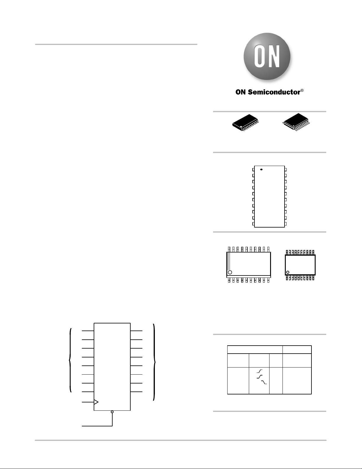
LOGIC DIAGRAM
2
Q0
5
Q1
6
Q2
9
Q3
Q4
Q5
Q6
Q7
NONINVERTING
OUTPUTS
12
15
16
19
DATA
INPUTS
D0
D1
D2
D3
D4
D5
D6
D7
CLOCK
3
4
7
8
13
14
17
18
11
http://onsemi.com
SOIC−20
DW SUFFIX
CASE 751D
TSSOP−20
DT SUFFIX
CASE 948E
PIN ASSIGNMENT
20
OUTPUT ENABLE
Q0
D0
D1
Q1
Q2
D2
D3
Q3
GND
1
2
3
4
5
6
7
8
9
10
V
CC
19
Q7
18
D7
17
D6
16
Q6
15
Q5
14
D5
13
D4
12
Q4
11
CLOCK
MARKING DIAGRAMS
20
HCT374A
AWLYYWWG
1
SOIC−20
A = Assembly Location
WL, L = Wafer Lot
YY, Y = Year
WW, W = Work Week
G or G = Pb−Free Package
(Note: Microdot may be in either location)
20
1
TSSOP−20
FUNCTION TABLE
Inputs Output
Output
Enable Clock D Q
LHH
LLL
L L,H, X No Change
HXXZ
X = don’t care
Z = high impedance
HCT
374A
ALYWG
G
OUTPUT ENABLE
© Semiconductor Components Industries, LLC, 2014
September, 2014 − Rev. 12
1
PIN 20 = V
PIN 10 = GND
CC
See detailed ordering and shipping information on page 5 o
ORDERING INFORMATION
this data sheet.
1 Publication Order Number:
MC74HCT374A/D
Page 2
MC74HCT374A
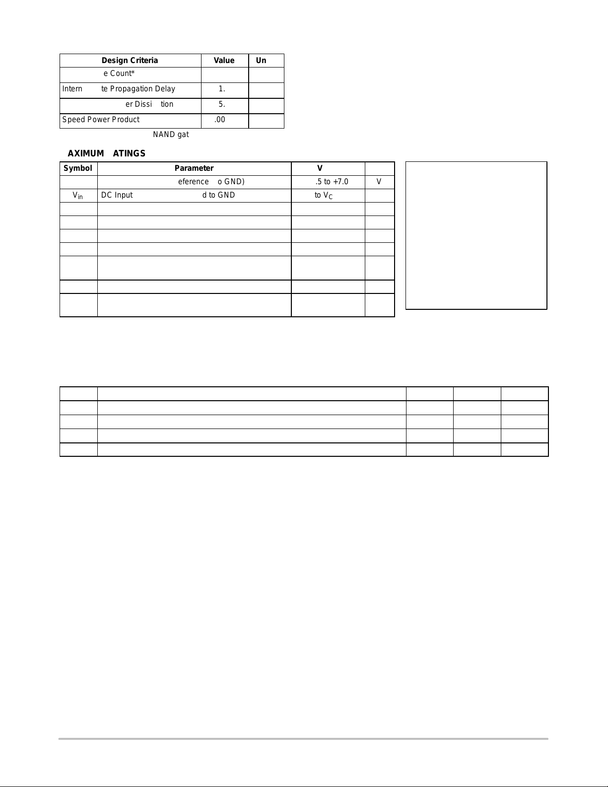
Design Criteria
Internal Gate Count*
Internal Gate Propagation Delay
Internal Gate Power Dissipation
Speed Power Product
Value
69
1.5
5.0
.0075
Units
ea.
ns
mW
pJ
*Equivalent to a two−input NAND gate.
MAXIMUM RATINGS
Symbol Parameter Value Unit
V
V
T
Stresses exceeding those listed in the Maximum Ratings table may damage the device. If any of
these limits are exceeded, device functionality should not be assumed, damage may occur and
reliability may be affected.
†Derating: SOIC Package: –7 mW/_C from 65_ to 125_C
DC Supply Voltage (Referenced to GND) –0.5 to +7.0 V
CC
V
DC Input Voltage (Referenced to GND) –0.5 to VCC + 0.5 V
in
DC Output Voltage (Referenced to GND) –0.5 to VCC + 0.5 V
out
I
DC Input Current, per Pin ±20 mA
in
I
DC Output Current, per Pin ±35 mA
out
I
DC Supply Current, VCC and GND Pins ±75 mA
CC
P
Power Dissipation in Still Air, SOIC Package†
D
TSSOP Package†
Storage Temperature –65 to +150
stg
T
Lead Temperature, 1 mm from Case for 10 Seconds
L
(SOIC or TSSOP Package)
TSSOP Package: −6.1 mW/_C from 65_ to 125_C
500
450
260
mW
_C
_C
This device contains protection
circuitry to guard against damage
due to high static voltages or electric
fields. However, precautions must
be taken to avoid applications of any
voltage higher than maximum rated
voltages to this high−impedance circuit. For proper operation, V
V
should be constrained to the
out
range GND v (V
or V
in
) v VCC.
out
in
and
Unused inputs must always be
tied to an appropriate logic voltage
level (e.g., either GND or V
CC
Unused outputs must be left open.
).
RECOMMENDED OPERATING CONDITIONS
Symbol Parameter Min Max Unit
V
Vin, V
tr, tfInput Rise and Fall Time (Figure 1) 0 500 ns
Functional operation above the stresses listed in the Recommended Operating Ranges is not implied. Extended exposure to stresses beyond
the Recommended Operating Ranges limits may affect device reliability.
DC Supply Voltage (Referenced to GND) 4.5 5.5 V
CC
DC Input Voltage, Output Voltage (Referenced to GND) 0 V
out
T
Operating Temperature, All Package Types –55 +125
A
CC
V
_C
http://onsemi.com
2
Page 3
MC74HCT374A
l
l
DC ELECTRICAL CHARACTERISTICS (Voltages Referenced to GND)
Symbo
V
Minimum High−Level Input Voltage V
IH
V
Maximum Low−Level Input Voltage V
IL
V
V
Minimum High−Level Output Voltage
OH
Maximum Low−Level Output Voltage
OL
I
Maximum Input Leakage Current Vin = VCC or GND 5.5 ±0.1 ±1.0 ±1.0
in
I
Maximum Three−State Leakage
OZ
Current
I
Maximum Quiescent Supply Current
CC
(per Package)
DI
Additional Quiescent Supply Current Vin = 2.4 V, Any One Input
CC
1. Total Supply Current = ICC + ΣDICC.
Parameter Test Conditions
= 0.1 V or VCC – 0.1 V
out
|I
| ≤ 20 mA
out
= 0.1 V or VCC – 0.1 V
out
|I
| ≤ 20 mA
out
Vin = VIH or V
|I
| ≤ 20 mA
out
Vin = VIH or V
|I
| ≤ 6.0 mA 4.5 3.98 3.84 3.7
out
Vin = VIH or V
|I
| ≤ 20 mA
out
Vin = VIH or V
|I
| ≤ 6.0 mA 4.5 0.26 0.33 0.4
out
IL
IL
IL
IL
Output in High−Impedance State
= VIL or V
V
in
V
= VCC or GND
out
IH
Vin = VCC or GND
I
= 0 mA
out
V
= VCC or GND, Other Inputs
in
= 0 mA
l
out
Guaranteed Limit
CC
V
4.5
5.5
4.5
5.5
4.5
5.5
4.5
5.5
−55 to
25_C
2.0
2.0
0.8
0.8
4.4
5.4
0.1
0.1
≤ 85_C ≤ 125_C
2.0
2.0
0.8
0.8
4.4
5.4
0.1
0.1
2.0
2.0
0.8
0.8
4.4
5.4
0.1
0.1
V
5.5 ±0.5 ±5.0 ±10
5.5 4.0 40 160
≥ −55_C 25_C to 125_C
5.5
2.9 2.4
Unit
V
V
V
V
mA
mA
mA
mA
AC ELECTRICAL CHARACTERISTICS (V
Symbo
f
Maximum Clock Frequency (50% Duty Cycle)
max
= 5.0 V ±10%, CL = 50 pF, Input tr = tf = 6.0 ns)
CC
Parameter
(Figures 1 and 4)
t
,
PLH
t
t
t
t
t
t
TLH
t
C
Maximum Propagation Delay, Clock to Q
PHL
PLZ
PHZ
PZL
PZH
THL
C
out
in
(Figures 1 and 4)
,
Maximum Propagation Delay, Output Enable to Q
(Figures 2 and 5)
,
Maximum Propagation Delay, Output Enable to Q
(Figures 2 and 5)
,
Maximum Output Transition Time, Any Output
(Figures 1 and 4)
Maximum Input Capacitance 10 10 10 pF
Maximum Three−State Output Capacitance
(Output in High−Impedance State)
C
Power Dissipation Capacitance (Per Flip−Flop)* 65 pF
PD
*Used to determine the no−load dynamic power consumption: PD = CPD V
2
f + ICC VCC.
CC
Guaranteed Limit
−55 to 25_C ≤ 85_C ≤ 125_C
30 24 20 MHz
31 39 47 ns
30 38 45 ns
30 38 45 ns
12 15 18 ns
15 15 15 pF
Typical @ 25°C, VCC = 5.0 V
Unit
http://onsemi.com
3
Page 4

MC74HCT374A
l
TIMING REQUIREMENTS (V
= 5.0 V ± 10%, Input tr = tf = 6.0 ns)
CC
Symbo
t
Minimum Setup Time, Data to Clock
su
(Figure 3)
t
Minimum Hold Time, Clock to Data
h
(Figure 3)
t
Minimum Pulse Width, Clock
w
(Figure 1)
tr, tfMaximum Input Rise and Fall Times
(Figure 1)
CLOCK
t
r
2.7 V
1.3 V
0.3 V
t
w
t
90%
1.3 V
Q
10%
PLH
t
TLH
t
f
1/f
max
t
PHL
Parameter
t
THL
SWITCHING WAVEFORMS
V
CC
GND
OUTPUT
ENABLE
Q
Q
Guaranteed Limit
−55 to 25_C ≤ 85_C ≤ 125_C
12 15 18 ns
5.0 5.0 5.0 ns
12 15 18 ns
500 500 500 ns
1.3 V
t
t
PLZ
PZL
1.3 V
10%
t
PZHtPHZ
90%
1.3 V
Unit
3 V
GND
HIGH
IMPEDANCE
V
OL
V
OH
HIGH
IMPEDANCE
DEVICE
UNDER
TEST
Figure 1.
TEST POINT
OUTPUT
CL*
DATA
CLOCK
VALID
1.3 V
t
su
1.3 V
Figure 3.
TEST CIRCUITS
DEVICE
UNDER
TEST
Figure 2.
3 V
t
h
OUTPUT
GND
3 V
GND
TEST POINT
1 kW
CL*
CONNECT TO VCC WHEN
TESTING t
PLZ
AND t
PZL
CONNECT TO GND WHEN
TESTING t
PHZ
AND t
PZH
*Includes all probe and jig capacitance
Figure 4.
*Includes all probe and jig capacitance
Figure 5.
http://onsemi.com
4
Page 5

MC74HCT374A
EXPANDED LOGIC DIAGRAM
D0 D1 D2 D3 D4 D5 D6 D7
347813141718
DQ
DQ
DQ
DQ
DQ
DQ
DQ
DQ
CLOCK
OUTPUT
ENABLE
C
11
1
C
256912151619
Q0 Q1 Q2 Q3 Q4 Q5 Q6 Q7
C
C
C
C
C
C
ORDERING INFORMATION
Device Package Shipping
MC74HCT374ADWG SOIC−20
(Pb−Free)
MC74HCT374ADWR2G SOIC−20
(Pb−Free)
MC74HCT374ADTR2G TSSOP−20
(Pb−Free)
†For information on tape and reel specifications, including part orientation and tape sizes, please refer to our Tape and Reel Packaging
Specifications Brochure, BRD8011/D.
38 Units / Rail
1000 Units / Reel
2500 Units / Reel
†
http://onsemi.com
5
Page 6
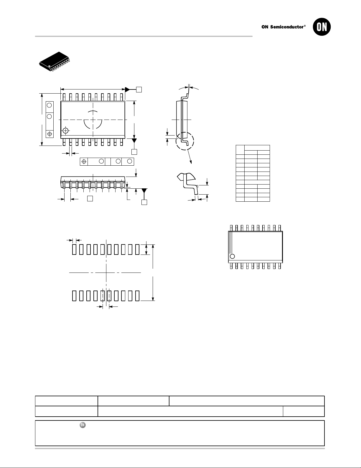
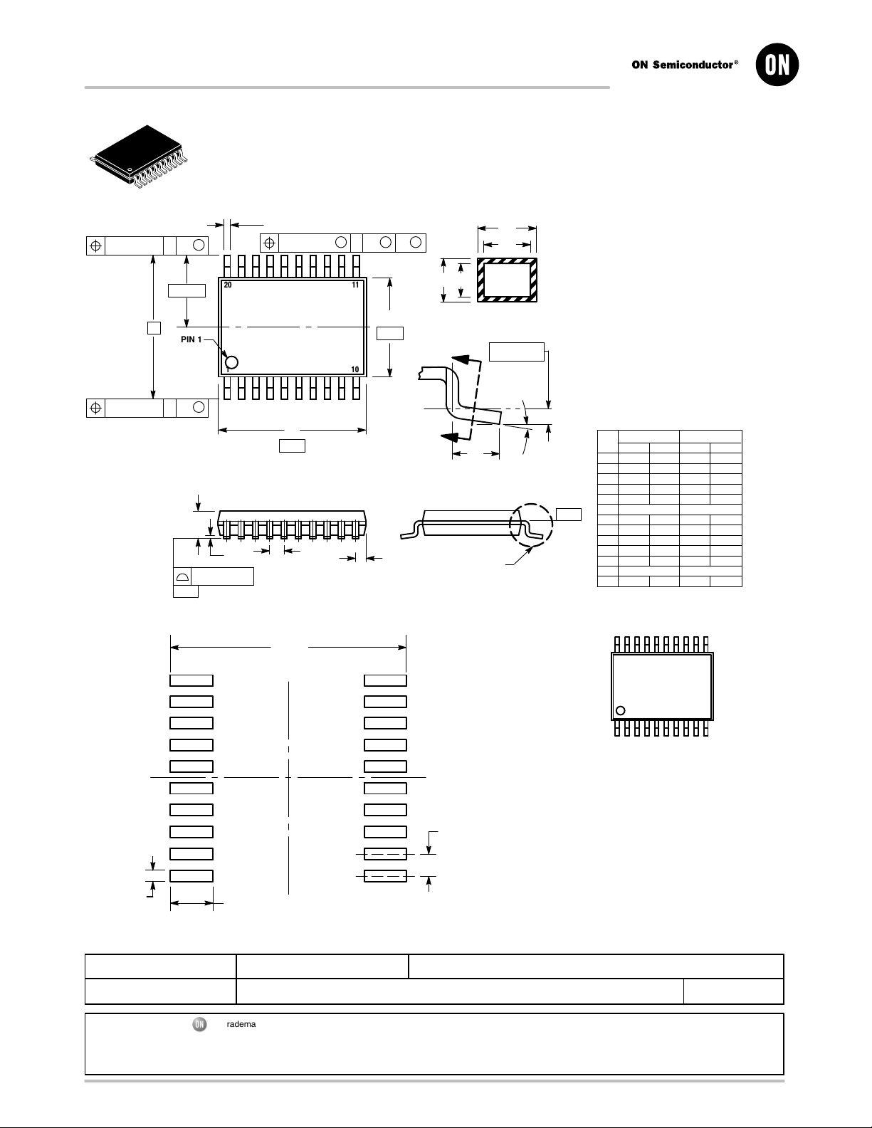
MECHANICAL CASE OUTLINE
PACKAGE DIMENSIONS
SCALE 1:1
D
20
M
B
M
H
0.25
1
b20X
M
SAS
T
0.25
18X
e
RECOMMENDED
SOLDERING FOOTPRINT*
20X
0.52
20 11
A
11
E
10
B
B
A
A1
T
20X
1.30
SOIC−20 WB
CASE 751D−05
SEATING
PLANE
ISSUE H
_
h X 45
DATE 22 APR 2015
q
NOTES:
1. DIMENSIONS ARE IN MILLIMETERS.
2. INTERPRET DIMENSIONS AND TOLERANCES
PER ASME Y14.5M, 1994.
3. DIMENSIONS D AND E DO NOT INCLUDE MOLD
PROTRUSION.
4. MAXIMUM MOLD PROTRUSION 0.15 PER SIDE.
5. DIMENSION B DOES NOT INCLUDE DAMBAR
PROTRUSION. ALLOWABLE PROTRUSION
SHALL BE 0.13 TOTAL IN EXCESS OF B
DIMENSION AT MAXIMUM MATERIAL
CONDITION.
MILLIMETERS
DIM MIN MAX
A 2.35 2.65
A1 0.10 0.25
b 0.35 0.49
c 0.23 0.32
D 12.65 12.95
E 7.40 7.60
e 1.27 BSC
L
c
H 10.05 10.55
h 0.25 0.75
L 0.50 0.90
q 0 7
__
GENERIC
MARKING DIAGRAM*
20
XXXXXXXXXXX
XXXXXXXXXXX
AWLYYWWG
11.00
1
XXXXX = Specific Device Code
1
10
A = Assembly Location
WL = Wafer Lot
YY = Year
1.27
PITCH
DIMENSIONS: MILLIMETERS
*For additional information on our Pb−Free strategy and soldering
details, please download the ON Semiconductor Soldering and
Mounting Techniques Reference Manual, SOLDERRM/D.
DOCUMENT NUMBER:
DESCRIPTION:
ON Semiconductor and are trademarks of Semiconductor Components Industries, LLC dba ON Semiconductor or its subsidiaries in the United States and/or other countries.
ON Semiconductor reserves the right to make changes without further notice to any products herein. ON Semiconductor makes no warranty, representation or guarantee regarding
the suitability of its products for any particular purpose, nor does ON Semiconductor assume any liability arising out of the application or use of any product or circuit, and specifically
disclaims any and all liability, including without limitation special, consequential or incidental damages. ON Semiconductor does not convey any license under its patent rights nor the
rights of others.
98ASB42343B
SOIC−20 WB
Electronic versions are uncontrolled except when accessed directly from the Document Repository.
Printed versions are uncontrolled except when stamped “CONTROLLED COPY” in red.
WW = Work Week
G = Pb−Free Package
*This information is generic. Please refer to
device data sheet for actual part marking.
Pb−Free indicator, “G” or microdot “ G”,
may or may not be present.
PAGE 1 OF 1
© Semiconductor Components Industries, LLC, 2019
www.onsemi.com
Page 7
MECHANICAL CASE OUTLINE
PACKAGE DIMENSIONS
TSSOP−20 WB
CASE 948E
ISSUE D
DATE 17 FEB 2016
SCALE 2:1
L
20X REFK
S
U0.15 (0.006) T
2X
L/2
PIN 1
IDENT
110
S
U0.15 (0.006) T
C
D
0.100 (0.004)
SEATING
−T−
PLANE
SOLDERING FOOTPRINT
1
0.10 (0.004) V
M
S
U
T
1120
−U−
A
−V−
G
H
7.06
NOTES:
S
K1
JJ1
K
B
SECTION N−N
N
0.25 (0.010)
M
N
F
DETAIL E
DETAIL E
1. DIMENSIONING AND TOLERANCING PER
ANSI Y14.5M, 1982.
2. CONTROLLING DIMENSION: MILLIMETER.
3. DIMENSION A DOES NOT INCLUDE MOLD
FLASH, PROTRUSIONS OR GATE BURRS.
MOLD FLASH OR GATE BURRS SHALL NOT
EXCEED 0.15 (0.006) PER SIDE.
4. DIMENSION B DOES NOT INCLUDE
INTERLEAD FLASH OR PROTRUSION.
INTERLEAD FLASH OR PROTRUSION
SHALL NOT EXCEED 0.25 (0.010) PER SIDE.
5. DIMENSION K DOES NOT INCLUDE
DAMBAR PROTRUSION. ALLOWABLE
DAMBAR PROTRUSION SHALL BE 0.08
(0.003) TOTAL IN EXCESS OF THE K
DIMENSION AT MAXIMUM MATERIAL
CONDITION.
6. TERMINAL NUMBERS ARE SHOWN FOR
REFERENCE ONLY.
7. DIMENSION A AND B ARE TO BE
DETERMINED AT DATUM PLANE −W−.
INCHES
6.60 0.260
−W−
MILLIMETERS
DIMAMIN MAX MIN MAX
6.40 0.252
B 4.30 4.50 0.169 0.177
C 1.20 0.047
--- ---
D 0.05 0.15 0.002 0.006
F 0.50 0.75 0.020 0.030
G 0.65 BSC 0.026 BSC
H 0.27 0.37 0.011 0.015
J 0.09 0.20 0.004 0.008
J1 0.09 0.16 0.004 0.006
K 0.19 0.30 0.007 0.012
K1 0.19 0.25 0.007 0.010
L 6.40 BSC 0.252 BSC
M 0 8 0 8
____
GENERIC
MARKING DIAGRAM*
XXXX
XXXX
ALYWG
G
A = Assembly Location
L = Wafer Lot
Y = Year
W = Work Week
G = Pb−Free Package
0.65
PITCH
(Note: Microdot may be in either location)
*This information is generic. Please refer to
device data sheet for actual part marking.
16X
0.36
DOCUMENT NUMBER:
DESCRIPTION:
ON Semiconductor and are trademarks of Semiconductor Components Industries, LLC dba ON Semiconductor or its subsidiaries in the United States and/or other countries.
ON Semiconductor reserves the right to make changes without further notice to any products herein. ON Semiconductor makes no warranty, representation or guarantee regarding
the suitability of its products for any particular purpose, nor does ON Semiconductor assume any liability arising out of the application or use of any product or circuit, and specifically
disclaims any and all liability, including without limitation special, consequential or incidental damages. ON Semiconductor does not convey any license under its patent rights nor the
rights of others.
© Semiconductor Components Industries, LLC, 2019
16X
1.26
98ASH70169A
TSSOP−20 WB
DIMENSIONS: MILLIMETERS
Electronic versions are uncontrolled except when accessed directly from the Document Repository.
Printed versions are uncontrolled except when stamped “CONTROLLED COPY” in red.
Pb−Free indicator, “G” or microdot “ G”,
may or may not be present.
PAGE 1 OF 1
www.onsemi.com
Page 8

ON Semiconductor and are trademarks of Semiconductor Components Industries, LLC dba ON Semiconductor or its subsidiaries in the United States and/or other countries.
ON Semiconductor owns the rights to a number of patents, trademarks, copyrights, trade secrets, and other intellectual property. A listing of ON Semiconductor’s product/patent
coverage may be accessed at www.onsemi.com/site/pdf/Patent−Marking.pdf
ON Semiconductor makes no warranty, representation or guarantee regarding the suitability of its products for any particular purpose, nor does ON Semiconductor assume any liability
arising out of the application or use of any product or circuit, and specifically disclaims any and all liability, including without limitation special, consequential or incidental damages.
Buyer is responsible for its products and applications using ON Semiconductor products, including compliance with all laws, regulations and safety requirements or standards,
regardless of any support or applications information provided by ON Semiconductor. “Typical” parameters which may be provided in ON Semiconductor data sheets and/or
specifications can and do vary in different applications and actual performance may vary over time. All operating parameters, including “Typicals” must be validated for each customer
application by customer’s technical experts. ON Semiconductor does not convey any license under its patent rights nor the rights of others. ON Semiconductor products are not
designed, intended, or authorized for use as a critical component in life support systems or any FDA Class 3 medical devices or medical devices with a same or similar classification
in a foreign jurisdiction or any devices intended for implantation in the human body. Should Buyer purchase or use ON Semiconductor products for any such unintended or unauthorized
application, Buyer shall indemnify and hold ON Semiconductor and its officers, employees, subsidiaries, affiliates, and distributors harmless against all claims, costs, damages, and
expenses, and reasonable attorney fees arising out of, directly or indirectly, any claim of personal injury or death associated with such unintended or unauthorized use, even if such
claim alleges that ON Semiconductor was negligent regarding the design or manufacture of the part. ON Semiconductor is an Equal Opportunity/Affirmative Action Employer. This
literature is subject to all applicable copyright laws and is not for resale in any manner.
. ON Semiconductor reserves the right to make changes without further notice to any products herein.
PUBLICATION ORDERING INFORMATION
LITERATURE FULFILLMENT:
Email Requests to: orderlit@onsemi.com
ON Semiconductor Website: www.onsemi.com
TECHNICAL SUPPORT
North American Technical Support:
Voice Mail: 1 800−282−9855 Toll Free USA/Canada
Phone: 011 421 33 790 2910
Europe, Middle East and Africa Technical Support:
Phone: 00421 33 790 2910
For additional information, please contact your local Sales Representative
◊
www.onsemi.com
1
 Loading...