

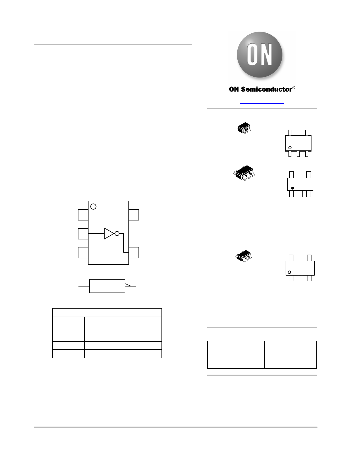
Single Unbuffered Inverter
MC74HC1GU04
The MC74HC1GU04 is a single unbuffered inverter in tiny
footprint packages.
The MC74HC1G0U04 output drive current is 1/2 compared to
MC74HC series.
Features
• High Speed: t
• Low Power Dissipation: I
• High Noise Immunity
• Balanced Propagation Delays (t
• Symmetrical Output Impedance (I
• Chip Complexity: < 100 FETs
• NLV Prefix for Automotive and Other Applications Requiring
Unique Site and Control Change Requirements; AEC−Q100
Qualified and PPAP Capable
• These Devices are Pb−Free, Halogen Free/BFR Free and are RoHS
Compliant
= 7 ns (Typ) at VCC = 5 V
PD
= 1 mA (Max) at TA = 25°C
CC
= t
pLH
OH
)
pHL
= IOL = 2 mA)
www.onsemi.com
SC−88A / SOT−353 / SC−70
DF SUFFIX
CASE 419A−02
TSOP−5 / SOT−23 / SC−59
DT SUFFIX
CASE 483
MARKING
DIAGRAMS
5
M
XX MG
G
1
5
XX MG
G
1
5
NC
GND
1
2
A
3
V
CC
Y
4
Figure 1. Pinout
A
1
Y
Figure 2. Logic Symbol
PIN ASSIGNMENT
1
2
3 GND
4
5V
NC
A
Y
CC
XX = Device Code
M = Date Code*
G = Pb−Free Package
(Note: Microdot may be in either location)
*Date Code orientation and/or position may vary
depending upon manufacturing location.
5
1
SC−74A
DBV SUFFIX
CASE 318BQ
XXX = Specific Device Code
M = Date Code
G = Pb−Free Package
(Note: Microdot may be in either location)
XXX MG
G
FUNCTION TABLE
Input A Output Y
L
H
H
L
© Semiconductor Components Industries, LLC, 2012
January, 2021 − Rev. 13
ORDERING INFORMATION
See detailed ordering, marking and shipping information in
the package dimensions section on page 6 of this data
sheet.
1 Publication Order Number:
MC74HC1GU04/D
MC74HC1GU04
MAXIMUM RATINGS
Symbol Parameter Value Unit
V
CC
V
IN
V
OUT
I
IK
I
OK
I
OUT
ICC or I
T
STG
T
L
T
J
q
JA
P
D
MSL Moisture Sensitivity Level 1
F
R
V
ESD
I
LATCHUP
Stresses exceeding those listed in the Maximum Ratings table may damage the device. If any of these limits are exceeded, device functionality
should not be assumed, damage may occur and reliability may be affected.
1. Measured with minimum pad spacing on an FR4 board, using 10 mm−by−1 inch, 20 ounce copper trace with no air flow per JESD51−7.
2. HBM tested to ANSI/ESDA/JEDEC JS−001−2017. CDM tested to JESD22−C101−F. JEDEC recommends that ESD qualification to
EIA/JESD22−A115A (Machine Model) be discontinued per JEDEC/JEP172A.
3. Tested to EIA/JESD78 Class II.
DC Supply Voltage TSOP−5
SC−88A, SC−74A
−0.5 to +7.0
−0.5 to +6.5
DC Input Voltage −0.5 to VCC )0.5 V
DC Output Voltage −0.5 to VCC )0.5 V
DC Input Diode Current ±20 mA
DC Output Diode Current ±20 mA
DC Output Source/Sink Current ±12.5 mA
DC Supply Current per Supply Pin or Ground Pin ±25 mA
GND
Storage Temperature Range −65 to +150 °C
Lead Temperature, 1 mm from Case for 10 Seconds 260 °C
Junction Temperature Under Bias +150 °C
Thermal Resistance (Note 1) SC−88A
SC−74A
Power Dissipation in Still Air at 85°CSC−88A
SC−74A
377
320
332
390
Flammability Rating Oxygen Index: 28 to 34 UL 94 V−0 @ 0.125 in
ESD Withstand Voltage (Note 2) Human Body Model
Charged Device Model
Latchup Performance (Note 3) TSOP−5
SC−88A, SC−74A
2000
1000
±500
±100
V
°C/W
mW
V
mA
www.onsemi.com
2
MC74HC1GU04
RECOMMENDED OPERATING CONDITIONS
Symbol Parameter Min Max Unit
V
CC
V
IN
V
OUT
T
t
, t
r
Functional operation above the stresses listed in the Recommended Operating Ranges is not implied. Extended exposure to stresses beyond
the Recommended Operating Ranges limits may affect device reliability.
DC ELECTRICAL CHARACTERISTICS
Symbol Parameter Test Conditions (V) Min Typ Max Min Max Min Max Unit
V
IH
V
IL
V
OH
V
OL
I
IN
I
CC
DC Supply Voltage 2.0 6.0 V
DC Input Voltage 0.0 V
DC Output Voltage 0.0 V
Operating Temperature Range −55 +125 °C
A
Input Rise and Fall Time TSOP−5
f
V
= 2.0 V
CC
VCC = 3.0 V
VCC = 4.5 V
V
= 6.0 V
CC
0
0
0
0
Input Rise and Fall Time SC−88A, SC−74A
V
High−Level Input
Voltage
Low−Level Input
Voltage
High−Level Output
Voltage
Low−Level Output
Voltage
Input Leakage
Current
Quiescent Supply
Current
VIN = VIH or V
IOH = −20 mA
VIN = GND
IOH = −2 mA
IOH = −2.6 mA
VIN = VIH or V
IOL = 20 mA
VIN = V
CC
IOL = 2 mA
IOL = 2.6 mA
VIN = 6.0 V or
GND
VIN = VCC or
GND
= 2.0 V to 2.7 V
CC
VCC = 3.0 V to 3.6 V
VCC = 4.5 V to 6.0 V
V
CC
2.0
3.0
4.5
6.0
2.0
3.0
4.5
6.0
2.0
IL
3.0
4.5
6.0
TA = 255C −40°C ≤ TA ≤ 85°C −55°C ≤ TA ≤ 125°C
1.7
2.45
3.6
4.8
1.8
2.7
4.0
5.5
−
−
−
−
−
−
−
−
−
−
2.0
3.0
4.5
6.0
0.3
−
0.5
−
0.9
−
1.2
−
−
−
−
−
−
−
1.7
2.45
3.6
4.8
−
−
−
−
1.8
2.7
4.0
5.5
−
4.5
4.18
6.0
5.68
5.76
2.0
IL
3.0
4.5
6.0
−
0.0
−
0.0
−
0.0
−
0.0
−
4.33
4.5
6.0
−−0.17
0.18
−
−
0.1
0.1
0.1
0.1
0.26
0.26
4.13
5.63
−
−
−
−
−
−
−
6.0 − − ±0.1 − ±1.0 − ±1.0
6.0 − − 1.0 − 10 − 40
−
−
−
−
0.3
0.5
0.9
1.2
−
−
−
−
−
−
−
0.1
0.1
0.1
0.1
0.33
0.33
0
0
0
1.7
2.45
3.6
4.8
−
−
−
−
1.8
2.7
4.0
5.5
4.08
5.58
−
−
−
−
−
−
−
CC
CC
1000
600
500
400
20
10
5
−
−
−
−
0.3
0.5
0.9
1.2
−
−
−
−
−
−
−
0.1
0.1
0.1
0.1
0.40
0.40
V
V
ns
ns/V
V
V
V
V
mA
mA
www.onsemi.com
3

MC74HC1GU04
AC ELECTRICAL CHARACTERISTICS
TA = 255C −40°C ≤ TA ≤ 85°C −55°C ≤ TA ≤ 125°C
Symbol Parameter Test Conditions Min Typ Max Min Max Min Max Unit
t
,
t
t
t
C
PLH
TLH
C
Propagation Delay,
A to Y
PHL
,
Output Transition
Time
THL
Input Capacitance − 5 10 − 10 − 10 pF
IN
Power Dissipation Capacitance (Note 4) 10 pF
PD
4. CPD is defined as the value of the internal equivalent capacitance which is calculated from the operating current consumption without load.
Average operating current can be obtained by the equation: I
power consumption; P
D
VCC = 5.0 V CL = 15 pF − 3 15 − 20 − 25 ns
VCC = 2.0 V CL = 50 pF
V
= 3.0 V
CC
VCC = 4.5 V
VCC = 6.0 V
−
17
−
100
9
6.5
27
7
20
17
−
−
−
−
−
−
125
35
25
21
−
−
−
−
VCC = 5.0 V CL = 15 pF − 4 10 − 15 − 20 ns
VCC = 2.0 V CL = 50 pF
V
= 3.0 V
CC
VCC = 4.5 V
VCC = 6.0 V
−
25
−
125
16
12
10
35
25
21
−
−
−
−
−
−
155
45
31
26
−
−
−
−
Typical @ 255C, VCC = 5.0 V
= CPD VCC fin + ICC. CPD is used to determine the no−load dynamic
)
= CPD V
2
fin + ICC VCC.
CC
CC(OPR
155
90
35
26
200
60
38
32
www.onsemi.com
4

MC74HC1GU04
OPEN
V
CC
R
GND
L
DUT
R
T
C
L*
*CL includes probe and jig capacitance
is Z
R
T
f = 1 MHz
of pulse generator (typically 50 W)
OUT
Figure 3. Test Circuit
tr = 6 ns tf = 6 ns
INPUT
OUTPUT
OUTPUT
10%
90%
V
mi
t
PHL
V
H
t
PLH
t
TLH
V
L
90%
V
mi
10%
t
PLH
t
TLH
V
mo
V
L
t
THL
V
H
V
mo
V
L
t
PHL
V
H
OUTPUT
V
H
V
mo
V
mo
V
L
t
THL
V
CC
GND
V
OH
V
OL
V
OH
V
OL
Test
t
/ t
PLH
t
/ t
TLH
(Note 5)
t
/ t
PLZ
t
/ t
PHZ
X − Don’t Care
INPUT
OUTPUT
OUTPUT
PHL
THL
PZL
PZH
Switch
Position
Open
Open X
V
CC
CL, pF
See AC Characteristics
Table
GND 1 k
V
mi
t
PZL
V
mo
t
PZH
V
mo
V
mi
t
PLZ
t
PHZ
RL, W
1 k
VOL + V
VOH - V
X
V
GND
~ V
V
V
~0 V
CC
CC
Y
OL
OH
Y
Figure 4. Switching Waveforms
Vmo, V
VCC, V Vmi, V
PLH
, t
PHLtPZL
, t
, t
PZH
, t
PLZ
t
3.0 to 3.6 VCC/2 VCC/2 VCC/2 V
4.5 to 5.5 VCC/2 VCC/2 VCC/2 V
5. t
TLH
and t
are measured from 10% to 90% of (VOH − VOL), and 90% to 10% of (VOH − VOL), respectively.
THL
www.onsemi.com
PHZ
5
VL, V VH, V VY, V
OL
OL
+ 0.1 (V
+ 0.1 (V
− VOL) V
OH
− VOL) V
OH
OL
OL
+ 0.9 (V
+ 0.9 (V
− VOL) 0.3
OH
− VOL) 0.3
OH

MC74HC1GU04
ORDERING INFORMATION
Pin 1 Orientation
Device Packages Marking
MC74HC1GU04DFT1G SC−88A H6 Q2 3000 / Tape & Reel
MC74HC1GU04DFT2G SC−88A H6 Q4 3000 / Tape & Reel
MC74HC1GU04DTT1G TSOP−5 H6 Q4 3000 / Tape & Reel
MC74HC1GU04DBVT1G SC−74A H6 Q4 3000 / Tape & Reel
†For complete information on tape and reel specifications, including part orientation and tape sizes, please refer to our Tape and Reel Packaging
Specifications Brochure, BRD8011/D.
*NLV Prefix for Automotive and Other Applications Requiring Unique Site and Control Change Requirements; AEC−Q100 Qualified and PPAP
Capable.
(See below)
Shipping
Pin 1 Orientation in Tape and Reel
†
www.onsemi.com
6

MECHANICAL CASE OUTLINE
PACKAGE DIMENSIONS
5
1
SCALE 2:1
b
5X
0.20
C AB
54
E1
123
B
A
D
TOP VIEW
SIDE VIEW
RECOMMENDED
SOLDERING FOOTPRINT*
0.95
PITCH
E
e
A
SEATING
C
PLANE
0.05
SC−74A
CASE 318BQ
ISSUE B
A1
DETAIL A
c
END VIEW
DATE 18 JAN 2018
NOTES:
1. DIMENSIONING AND TOLERANCING PER ASME
Y14.5M, 1994.
2. CONTROLLING DIMENSION: MILLIMETERS.
3. MAXIMUM LEAD THICKNESS INCLUDES LEAD FINISH
M
L
DETAIL A
THICKNESS. MINIMUM LEAD THICKNESS IS THE
MINIMUM THICKNESS OF BASE MATERIAL.
4. DIMENSIONS A AND B DO NOT INCLUDE MOLD
FLASH, PROTRUSIONS, OR GATE BURRS. MOLD
FLASH, PROTRUSIONS, OR GATE BURRS SHALL NOT
EXCEED 0.15 PER SIDE.
MILLIMETERS
DIM MIN MAX
A 0.90 1.10
A1 0.01 0.10
b 0.25 0.50
c 0.10 0.26
D
2.85 3.15
E 2.50 3.00
E1
1.35 1.65
e 0.95 BSC
L 0.20 0.60
M 0 10
__
GENERIC
MARKING DIAGRAM*
XXX MG
G
2.40
5X
1.00
5X
0.70
DIMENSIONS: MILLIMETERS
*For additional information on our Pb−Free strategy and soldering
details, please download the ON Semiconductor Soldering and
Mounting Techniques Reference Manual, SOLDERRM/D.
DOCUMENT NUMBER:
DESCRIPTION:
98AON66279G
SC−74A
XXX = Specific Device Code
M = Date Code
G = Pb−Free Package
(Note: Microdot may be in either location)
*This information is generic. Please refer to
device data sheet for actual part marking.
Pb−Free indicator, “G” or microdot “ G”,
may or may not be present. Some products
may not follow the Generic Marking.
Electronic versions are uncontrolled except when accessed directly from the Document Repository.
Printed versions are uncontrolled except when stamped “CONTROLLED COPY” in red.
PAGE 1 OF 1
ON Semiconductor and are trademarks of Semiconductor Components Industries, LLC dba ON Semiconductor or its subsidiaries in the United States and/or other countries.
ON Semiconductor reserves the right to make changes without further notice to any products herein. ON Semiconductor makes no warranty, representation or guarantee regarding
the suitability of its products for any particular purpose, nor does ON Semiconductor assume any liability arising out of the application or use of any product or circuit, and specifically
disclaims any and all liability, including without limitation special, consequential or incidental damages. ON Semiconductor does not convey any license under its patent rights nor the
rights of others.
© Semiconductor Components Industries, LLC, 2018
www.onsemi.com

MECHANICAL CASE OUTLINE
PACKAGE DIMENSIONS
SC−88A (SC−70−5/SOT−353)
SCALE 2:1
CASE 419A−02
ISSUE L
DATE 17 JAN 2013
S
0.40
0.0157
A
G
12 3
H
SOLDER FOOTPRINT
0.50
0.0197
D
NOTES:
1. DIMENSIONING AND TOLERANCING
PER ANSI Y14.5M, 1982.
2. CONTROLLING DIMENSION: INCH.
3. 419A−01 OBSOLETE. NEW STANDARD
419A−02.
4. DIMENSIONS A AND B DO NOT INCLUDE
45
−B−
MM
5 PL
B0.2 (0.008)
N
MOLD FLASH, PROTRUSIONS, OR GATE
BURRS.
INCHES
DIMAMIN MAX MIN MAX
B 1.15 1.350.045 0.053
C 0.80 1.100.031 0.043
D 0.10 0.300.004 0.012
G 0.65 BSC0.026 BSC
H --- 0.10---0.004
J 0.10 0.250.004 0.010
K 0.10 0.300.004 0.012
N 0.20 REF0.008 REF
S 2.00 2.200.079 0.087
MILLIMETERS
1.80 2.200.071 0.087
J
C
GENERIC MARKING
DIAGRAM*
K
XXXMG
G
XXX = Specific Device Code
M = Date Code
G = Pb−Free Package
0.65
0.025
0.65
0.025
(Note: Microdot may be in either location)
*This information is generic. Please refer to
device data sheet for actual part marking.
Pb−Free indicator, “G” or microdot “G”, may
or may not be present. Some products may
not follow the Generic Marking.
1.9
0.0748
STYLE 1:
PIN 1. BASE
2. EMITTER
3. BASE
4. COLLECTOR
5. COLLECTOR
STYLE 6:
PIN 1. EMITTER 2
2. BASE 2
3. EMITTER 1
4. COLLECTOR
5. COLLECTOR 2/BASE 1
DOCUMENT NUMBER:
DESCRIPTION:
ON Semiconductor and are trademarks of Semiconductor Components Industries, LLC dba ON Semiconductor or its subsidiaries in the United States and/or other countries.
ON Semiconductor reserves the right to make changes without further notice to any products herein. ON Semiconductor makes no warranty, representation or guarantee regarding
the suitability of its products for any particular purpose, nor does ON Semiconductor assume any liability arising out of the application or use of any product or circuit, and specifically
disclaims any and all liability, including without limitation special, consequential or incidental damages. ON Semiconductor does not convey any license under its patent rights nor the
rights of others.
© Semiconductor Components Industries, LLC, 2018
STYLE 2:
PIN 1. ANODE
2. EMITTER
3. BASE
4. COLLECTOR
5. CATHODE
STYLE 7:
PIN 1. BASE
2. EMITTER
3. BASE
4. COLLECTOR
5. COLLECTOR
98ASB42984B
SC−88A (SC−70−5/SOT−353)
SCALE 20:1
STYLE 3:
PIN 1. ANODE 1
2. N/C
3. ANODE 2
4. CATHODE 2
5. CATHODE 1
STYLE 8:
PIN 1. CATHODE
2. COLLECTOR
3. N/C
4. BASE
5. EMITTER
mm
ǒ
Ǔ
inches
STYLE 4:
PIN 1. SOURCE 1
2. DRAIN 1/2
3. SOURCE 1
4. GATE 1
5. GATE 2
STYLE 9:
PIN 1. ANODE
2. CATHODE
3. ANODE
4. ANODE
5. ANODE
Electronic versions are uncontrolled except when accessed directly from the Document Repository.
Printed versions are uncontrolled except when stamped “CONTROLLED COPY” in red.
STYLE 5:
PIN 1. CATHODE
2. COMMON ANODE
3. CATHODE 2
4. CATHODE 3
5. CATHODE 4
Note: Please refer to datasheet for
style callout. If style type is not called
out in the datasheet refer to the device
datasheet pinout or pin assignment.
PAGE 1 OF 1
www.onsemi.com

MECHANICAL CASE OUTLINE
PACKAGE DIMENSIONS
5
1
SCALE 2:1
NOTE 5
2X
2X
T0.10
B
A
54
B
123
G
A
T0.20
TOP VIEW
0.05
H
SIDE VIEW
D
0.205XC AB
S
C
SEATING
C
PLANE
TSOP−5
CASE 483
ISSUE N
K
J
END VIEW
DETAIL Z
M
DETAIL Z
DATE 12 AUG 2020
NOTES:
1. DIMENSIONING AND TOLERANCING PER ASME
Y14.5M, 1994.
2. CONTROLLING DIMENSION: MILLIMETERS.
3. MAXIMUM LEAD THICKNESS INCLUDES LEAD FINISH
THICKNESS. MINIMUM LEAD THICKNESS IS THE
MINIMUM THICKNESS OF BASE MATERIAL.
4. DIMENSIONS A AND B DO NOT INCLUDE MOLD
FLASH, PROTRUSIONS, OR GATE BURRS. MOLD
FLASH, PROTRUSIONS, OR GATE BURRS SHALL NOT
EXCEED 0.15 PER SIDE. DIMENSION A.
5. OPTIONAL CONSTRUCTION: AN ADDITIONAL
TRIMMED LEAD IS ALLOWED IN THIS LOCATION.
TRIMMED LEAD NOT TO EXTEND MORE THAN 0.2
FROM BODY.
MILLIMETERS
DIM MIN MAX
A
2.85 3.15
B
1.35 1.65
C 0.90 1.10
D 0.25 0.50
G 0.95 BSC
H 0.01 0.10
J 0.10 0.26
K 0.20 0.60
M 0 10
__
S 2.50 3.00
SOLDERING FOOTPRINT*
1.9
0.95
0.037
1.0
0.039
*For additional information on our Pb−Free strategy and soldering
details, please download the ON Semiconductor Soldering and
Mounting Techniques Reference Manual, SOLDERRM/D.
0.074
0.028
0.7
2.4
0.094
SCALE 10:1
ǒ
inches
mm
GENERIC
MARKING DIAGRAM*
5
XXXAYWG
G
1
Analog
XXX = Specific Device Code
A = Assembly Location
Y = Year
W = Work Week
G = Pb−Free Package
(Note: Microdot may be in either location)
Ǔ
*This information is generic. Please refer to
device data sheet for actual part marking.
Pb−Free indicator, “G” or microdot “ G”,
may or may not be present.
5
XXX MG
G
1
Discrete/Logic
XXX = Specific Device Code
M = Date Code
G = Pb−Free Package
DOCUMENT NUMBER:
DESCRIPTION:
ON Semiconductor and are trademarks of Semiconductor Components Industries, LLC dba ON Semiconductor or its subsidiaries in the United States and/or other countries.
ON Semiconductor reserves the right to make changes without further notice to any products herein. ON Semiconductor makes no warranty, representation or guarantee regarding
the suitability of its products for any particular purpose, nor does ON Semiconductor assume any liability arising out of the application or use of any product or circuit, and specifically
disclaims any and all liability, including without limitation special, consequential or incidental damages. ON Semiconductor does not convey any license under its patent rights nor the
rights of others.
© Semiconductor Components Industries, LLC, 2018
98ARB18753C
TSOP−5
Electronic versions are uncontrolled except when accessed directly from the Document Repository.
Printed versions are uncontrolled except when stamped “CONTROLLED COPY” in red.
PAGE 1 OF 1
www.onsemi.com

ON Semiconductor and are trademarks of Semiconductor Components Industries, LLC dba ON Semiconductor or its subsidiaries in the United States and/or other countries.
ON Semiconductor owns the rights to a number of patents, trademarks, copyrights, trade secrets, and other intellectual property. A listing of ON Semiconductor’s product/patent
coverage may be accessed at www.onsemi.com/site/pdf/Patent−Marking.pdf
ON Semiconductor makes no warranty, representation or guarantee regarding the suitability of its products for any particular purpose, nor does ON Semiconductor assume any liability
arising out of the application or use of any product or circuit, and specifically disclaims any and all liability, including without limitation special, consequential or incidental damages.
Buyer is responsible for its products and applications using ON Semiconductor products, including compliance with all laws, regulations and safety requirements or standards,
regardless of any support or applications information provided by ON Semiconductor. “Typical” parameters which may be provided in ON Semiconductor data sheets and/or
specifications can and do vary in different applications and actual performance may vary over time. All operating parameters, including “Typicals” must be validated for each customer
application by customer’s technical experts. ON Semiconductor does not convey any license under its patent rights nor the rights of others. ON Semiconductor products are not
designed, intended, or authorized for use as a critical component in life support systems or any FDA Class 3 medical devices or medical devices with a same or similar classification
in a foreign jurisdiction or any devices intended for implantation in the human body. Should Buyer purchase or use ON Semiconductor products for any such unintended or unauthorized
application, Buyer shall indemnify and hold ON Semiconductor and its officers, employees, subsidiaries, affiliates, and distributors harmless against all claims, costs, damages, and
expenses, and reasonable attorney fees arising out of, directly or indirectly, any claim of personal injury or death associated with such unintended or unauthorized use, even if such
claim alleges that ON Semiconductor was negligent regarding the design or manufacture of the part. ON Semiconductor is an Equal Opportunity/Affirmative Action Employer. This
literature is subject to all applicable copyright laws and is not for resale in any manner.
. ON Semiconductor reserves the right to make changes without further notice to any products herein.
PUBLICATION ORDERING INFORMATION
LITERATURE FULFILLMENT:
Email Requests to: orderlit@onsemi.com
ON Semiconductor Website: www.onsemi.com
TECHNICAL SUPPORT
North American Technical Support:
Voice Mail: 1 800−282−9855 Toll Free USA/Canada
Phone: 011 421 33 790 2910
Europe, Middle East and Africa Technical Support:
Phone: 00421 33 790 2910
For additional information, please contact your local Sales Representative
◊
www.onsemi.com
1
 Loading...