

查询MC33152DR2供应商
MC34152, MC33152,
NCV33152
High Speed Dual
MOSFET Drivers
The MC34152/MC33152 are dual noninverting high speed drivers
specifically designed for applications that require low current digital
signals to drive large capacitive loads with high slew rates. These
devices feature low input current making them CMOS/LSTTL logic
compatible, input hysteresis for fast output switching that is
independent of input transition time, and two high current totem pole
outputs ideally suited for driving power MOSFETs. Also included is
an undervoltage lockout with hysteresis to prevent system erratic
operation at low supply voltages.
Typical applications include switching power supplies, dc−to−dc
converters, capacitor charge pump voltage doublers/inverters, and
motor controllers.
This device is avail a ble in dual−in−line and surface mount packages.
Features
• Pb−Free Packages are Available
• Two Independent Channels with 1.5 A Totem Pole Outputs
• Output Rise and Fall Times of 15 ns with 1000 pF Load
• CMOS/LSTTL Compatible Inputs with Hysteresis
• Undervoltage Lockout with Hysteresis
• Low Standby Current
• Efficient High Frequency Operation
• Enhanced System Performance with Common Switching Regulator
Control ICs
• NCV Prefix for Automotive and Other Applications Requiring Site
and Control Changes
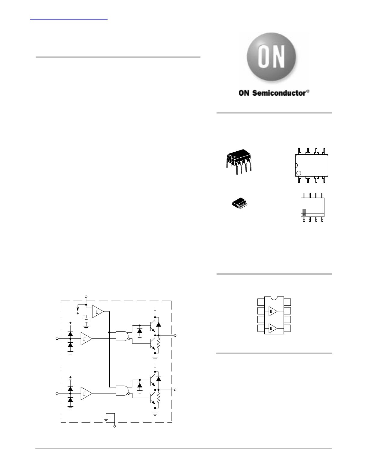
VCC6
+
−
5.7V
Drive Output A
Logic
Input A
2
100k
7
http://onsemi.com
MARKING
DIAGRAMS
8
PDIP−8
P SUFFIX
8
1
8
1
CASE 626
SOIC−8
D SUFFIX
CASE 751
x = 3 or 4
A = Assembly Location
WL, L = Wafer Lot
YY, Y = Year
WW, W = Work W eek
PIN CONNECTIONS
1 8 N.C.N.C.
2 7 Drive Output ALogic Input A
36V
GND
4 5 Drive Output BLogic Input B
(Top V iew)
MC3x152P
AWL
YYWW
1
8
3x152
ALYW
1
CC
Logic
Input B
4
GND 3
Figure 1. Representative Diagram
Semiconductor Components Industries, LLC, 2004
October, 2004 − Rev. 7
100k
ORDERING INFORMATION
See detailed ordering and shipping information in the package
dimensions section on page 2 of this data sheet.
Drive Output B
5
1 Publication Order Number:
MC34152/D
MC34152, MC33152, NCV33152
MAXIMUM RATINGS
Rating Symbol Value Unit
Power Supply Voltage V
Logic Inputs (Note 1) V
CC
in
Drive Outputs (Note 2)
Totem Pole Sink or Source Current
Diode Clamp Current (Drive Output to VCC)
I
O
I
O(clamp)
Power Dissipation and Thermal Characteristics
D Suffix, Plastic Package Case 751
Maximum Power Dissipation @ TA = 50°C
Thermal Resistance, Junction−to−Air
P
D
R
JA
P Suffix, Plastic Package, Case 626
Maximum Power Dissipation @ TA = 50°C
Thermal Resistance, Junction−to−Air
Operating Junction Temperature T
Operating Ambient Temperature MC34152
P
D
R
JA
J
T
A
Operating Ambient Temperature MC33152
Operating Ambient Temperature MC33152V, NCV33152
Storage Temperature Range T
Electrostatic Discharge Sensitivity (ESD)
stg
ESD
Human Body Model (HBM)
Machine Model (MM)
Maximum ratings are those values beyond which device damage can occur. Maximum ratings applied to the device are individual stress limit values
(not normal operating conditions) and are not valid simultaneously. If these limits are exceeded, device functional operation is not implied, damage
may occur and reliability may be affected.
1. For optimum switching speed, the maximum input voltage should be limited to 10 V or VCC, whichever is less.
2. Maximum package power dissipation limits must be observed.
20 V
−0.3 to +V
CC
1.5
1.0
0.56
180
°C/W
1.0
100
°C/W
+150 °C
0 to +70
−40to +85
−40to +125
−65to +150 °C
2000
200
V
A
W
W
°C
V
ORDERING INFORMATION
Device Package Shipping
MC34152D SOIC−8 98 Units / Rail
MC34152DG
SOIC−8
(Pb−Free)
98 Units / Rail
MC34152DR2 SOIC−8 2500 Tape & Reel
MC34152DR2G
SOIC−8
(Pb−Free)
2500 Tape & Reel
MC34152P PDIP−8 50 Units / Rail
MC33152D SOIC−8 98 Units / Rail
MC33152DR2 SOIC−8 2500 Tape & Reel
MC33152P PDIP−8 50 Units / Rail
MC33152PG
PDIP−8
(Pb−Free)
50 Units / Rail
MC33152VDR2 SOIC−8 2500 Tape & Reel
NCV33152DR2* SOIC−8 2500 Tape & Reel
NCV33152DR2G*
SOIC−8
(Pb−Free)
2500 Tape & Reel
†For information on tape and reel specifications, including part orientation and tape sizes, please refer to our Tape and Reel Packaging
Specifications Brochure, BRD8011/D.
*NCV prefix is for automotive and other applications requiring site and change control.
†
http://onsemi.com
2
MC34152, MC33152, NCV33152
ELECTRICAL CHARACTERISTICS (V
= 12 V, for typical values TA = 25°C, for min/max values TA is the operating ambient
CC
temperature range that applies [Note 3], unless otherwise noted.)
Characteristics Symbol Min Typ Max Unit
LOGIC INPUTS
Input Threshold Voltage
Output Transition High−to−Low State
Output Transition Low−to−High State
V
IH
V
IL
0.8
−
1.75
1.58
Input Current
High State (VIH = 2.6 V)
Low State (VIL = 0.8 V)
I
IH
I
IL
−
−
100
20
DRIVE OUTPUT
Output Voltage
Low State (I
Low State (I
Low State (I
High State (I
High State (I
High State (I
Output Pull−Down Resistor R
= 10 mA)
sink
= 50 mA)
sink
= 400 mA)
sink
source
source
source
= 10 mA)
= 50 mA)
= 400 mA)
V
OL
V
OH
PD
−
−
−
10.5
10.4
10
0.8
1.1
1.8
11.2
11.1
10.8
− 100 − k
SWITCHING CHARACTERISTICS (TA = 25°C)
Propagation Delay (CL = 1.0 nF)
Logic Input to: Drive Output Rise (10% Input to 10% Output)
Drive Output Fall (90% Input to 90% Output)
Drive Output Rise Time (10% to 90%) CL = 1.0 nF
Drive Output Rise Time (10% to 90%) CL = 2.5 nF
Drive Output Fall Time (90% to 10%) CL = 1.0 nF
Drive Output Fall Time (90% to 10%) CL = 2.5 nF
t
PLH (IN/OUT)
t
PHL (IN/OUT)
t
r
t
f
−
−
−
−
−
−
55
40
14
36
15
32
TOTAL DEVICE
Power Supply Current
Standby (Logic Inputs Grounded)
Operating (CL = 1.0 nF Drive Outputs 1 and 2, f = 100 kHz)
Operating Voltage V
I
CC
CC
−
−
6.0
10.5
6.5 − 18 V
3. Low duty cycle pulse techniques are used during test to maintain junction temperature as close to ambient as possible.
T
= 0°C for MC34152, −40°C for MC33152, −40°C for MC33152V
low
T
= +70°C for MC34152, +85°C for MC33152, +125°C for MC33152V
high
NCV33152: T
= −40°C, T
low
= +125°C. Guaranteed by design.
high
2.6
−
300
100
1.2
1.5
2.5
−
−
−
120
120
30
−
30
−
8.0
15
V
A
V
ns
ns
ns
mA
http://onsemi.com
3
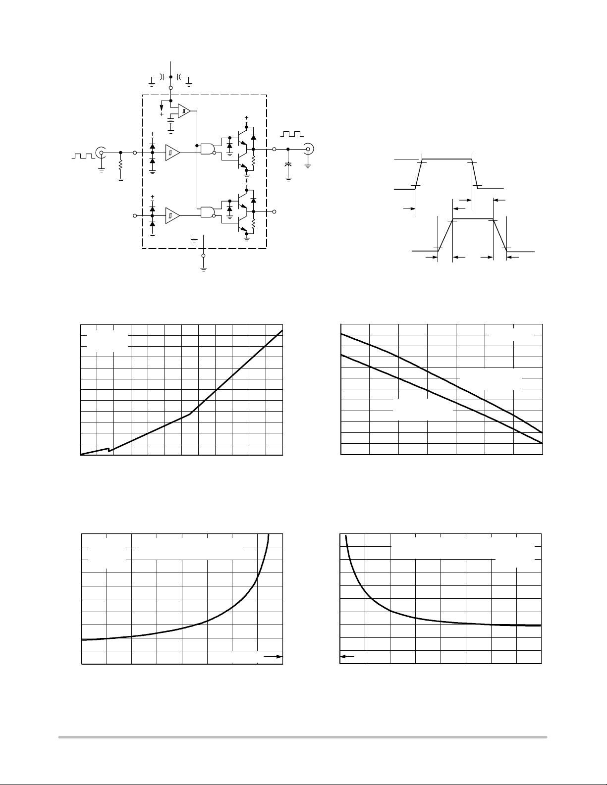
Logic Input
MC34152, MC33152, NCV33152
12V
0.14.7
+
6
+
−
+
5.7V
2
50
4
3
Drive Output
7
100k100k
5
C
L
Logic Input
tr, t
≤ 10 ns
f
5 V
0 V
10%
t
PLH
t
PHL
90%
10%
Drive Output
90%
t
r
t
f
Figure 2. Switching Characteristics Test CIrcuit
2.4
VCC=12V
T
=25°C
2.0
A
1.6
1.2
0.8
, INPUT CURRENT (mA)
in
I
0.4
0
0 2.0 4.0 6.0 8.0 10 12
Vin, INPUT VOLTAGE (V) T
2.2
2.0
1.8
1.6
1.4
1.2
, INPUT THRESHOLD VOLTAGE (V)
th
V
1.0
Figure 3. Switching Waveform Definitions
VCC=12V
Upper Threshold
Low State Output
Lower Threshold
High State Output
−55 −25 0 25 50 75 100 125
, AMBIENT TEMPERATURE (°C)
A
Figure 4. Logic Input Current versus Input Voltage Figure 5. Logic Input Threshold Voltage
versus Temperature
200
160
VCC=12V
CL=1.0nF
T
=25°C
A
Overdrive Voltage is with Respect
to the Logic Input Lower Threshold
200
160
Overdrive Voltage is with Respect
to the Logic InputUpperThreshold
VCC=12V
CL=1.0nF
T
=25°C
A
120
80
40
, DRIVE OUTPUT PROPAGATION DELAY (ns)
0
−1.6 −1.2 −0.8 −0.4 0
Vin, INPUT OVERDRIVE VOLTAGE BELOW LOWER THRESHOLD (V)
PLH(In/Out)
t
V
th(lower)
Figure 6. Drive Output High to Low Propagation
Delay versus Logic Input Overdrive Voltage
120
80
40
, DRIVE OUTPUT PROPAGATION DELAY (ns)
PHL(In/Out)
t
http://onsemi.com
4
V
th(upper)
0
0
1234
Vin, INPUT OVERDRIVE VOLTAGE ABOVE UPPER THRESHOLD (V)
Figure 7. Drive Output Low to High Propagation
Delay versus Logic Input Overdrive Voltage

90% −
VCC = 12 V
Vin = 0 V to 5.0 V
CL = 1.0 nF
T
= 25°C
A
Drive Output
MC34152, MC33152, NCV33152
3.0
High State Clamp (Drive
Output Driven Above VCC)
2.0
1.0
0
VCC = 12 V
80 s Pulsed Load
120 Hz Rate
T
= 25°C
A
V
CC
10% −
Logic Input
50 ns/DIV
Figure 8. Propagation Delay Figure 9. Drive Output Clamp Voltage
0
−1.0
−2.0
−3.0
3.0
2.0
1.0
sat
V , OUTPUT SATURATION VOLTAGE (V)
0
0 0.2 0.4 0.6 0.8 1.0 1.2 1.4
IO, OUTPUT CLAMP CURRENT (A)
V
CC
Sink Saturation
(Load to VCC)
Source Saturation
(Load to Ground)
VCC = 12 V
80 s Pulsed Load
120 Hz Rate
T
= 25°C
A
GND
, OUTPUT CLAMP VOLTAGE (V), OUTPUT SATURATION VOLTAGE (V)
0
clamp
V
−1.0
0 0.2 0.4 0.6 0.8 1.0 1.2 1.4
GND
Low State Clamp (Drive
Output Driven Below Ground)
IO, OUTPUT CLAMP CURRENT (A)
versus Clamp Current
0
Source Saturation
−0.5
−0.7
(Load to Ground)
VCC = 12 V
V
CC
−0.9
−1.1
1.9
1.7
1.5
1.0
0.8
sat
V
(Load to VCC)
0
−55 −25 0 25 50 75 100 125
Sink Saturation
0.6
GND
T
, AMBIENT TEMPERATURE (°C)
A
I
source
I
source
I
sink
I
= 10 mA
= 400 mA
= 400 mA
= 10 mA
sink
90% −
10% −
Figure 10. Drive Output Saturation Voltage
versus Load Current
Figure 11. Drive Output Saturation Voltage
versus Temperature
90% −
VCC = 12 V
Vin = 0 V to 5.0 V
CL = 1.0 nF
T
= 25°C
A
10% −
10 ns/DIV 10 ns/DIV
Figure 12. Drive Output Rise Time Figure 13. Drive Output Fall Time
http://onsemi.com
5
VCC = 12 V
Vin = 0 V to 5.0 V
CL = 1.0 nF
T
= 25°C
A

MC34152, MC33152, NCV33152
80
VCC = 12 V
VIN = 0 V to 5.0 V
T
= 25°C
60
A
40
t
, OUTPUT RISE-FALL TIME(ns)
f
20
−t
r
t
0
0.1 1.0 10
CL, OUTPUT LOAD CAPACITANCE (nF)
f
t
r
Figure 14. Drive Output Rise and Fall Time
versus Load Capacitance
80
Both Logic Inputs Driven
0 V to 5.0 V,
50% Duty Cycle
60
Both Drive Outputs Loaded
T
= 25°C
A
1 − VCC = 18 V, CL = 2.5 nF
2 − VCC = 12 V, CL = 2.5 nF
40
3 − VCC = 18 V, CL = 1.0 nF
4 − VCC = 12 V, CL = 1.0 nF
, SUPPLY CURRENT (mA)
20
CC
I
1
2
3
4
80
VCC = 12 V
Both Logic Inputs Driven
0 V to 5.0 V
60
50% Duty Cycle
Both Drive Outputs Loaded
T
= 25°C
A
40
f = 500 kHz
, SUPPLY CURRENT (mA)
20
CC
I
0
0.1 1.0 10
CL, OUTPUT LOAD CAPACITANCE (nF)
f = 200 kHz
f = 50 kHz
Figure 15. Supply Current versus Drive
Output Load Capacitance
8.0
T
= 25°C
A
6.0
4.0
, SUPPLY CURRENT (mA)
2.0
CC
I
Logic Inputs at V
Low State Drive Outputs
CC
Logic Inputs Grounded
High State Drive Outputs
0
10 k 100 1.0 M
f, INPUT FREQUENCY (Hz) VCC, SUPPLY VOLTAGE (V)
0
0 4.0 8.0 12 16
Figure 16. Supply Current versus Input Frequency Figure 17. Supply Current versus Supply Voltage
APPLICATIONS INFORMATION
Description
The MC34152 is a dual noninverting high speed driver
specifically designed to interface low current digital
circuitry with power MOSFETs. This device is constructed
with Schottky clamped Bipolar Analog technology which
offers a high degree of performance and ruggedness in
hostile industrial environments.
Input Stage
The Logic Inputs have 170 mV of hysteresis with the
input threshold centered at 1.67 V. The input thresholds are
insensitive to VCC making this device directly compatible
with CMOS and LSTTL logic families over its entire
operating voltage range. Input hysteresis provides fast
output switching that is independent of the input signal
transition time, preventing output oscillations as the input
thresholds are crossed. The inputs are designed to accept a
signal amplitude ranging from ground to VCC. This allows
the output of one channel to directly drive the input of a
second channel for master−slave operation. Each input has
a 30 k pulldown resistor so that an unconnected open
input will cause the associated Drive Output to be in a
known low state.
Output Stage
Each totem pole Drive Output is capable of sourcing and
sinking up to 1.5 A with a typical ‘on’ resistance of 2.4
at 1.0 A. The low ‘on’ resistance allows high output
currents to be attained at a lower VCC than with
comparative CMOS drivers. Each output has a 100 k
pulldown resistor to keep the MOSFET gate low when V
is less than 1.4 V. No over current or thermal protection has
been designed into the device, so output shorting to VCC or
ground must be avoided.
Parasitic inductance in series with the load will cause the
driver outputs to ring above VCC during the turn−on
transition, and below ground during the turn−off transition.
With CMOS drivers, this mode of operation can cause a
destructive output latchup condition. The MC34152 is
immune to output latchup. The Drive Outputs contain an
internal diode to VCC for clamping positive voltage
transients. When operating with VCC at 18 V, proper power
supply bypassing must be observed to prevent the output
ringing from exceeding the maximum 20 V device rating.
Negative output transients are clamped by the internal NPN
pullup transistor. Since full supply voltage is applied across
CC
http://onsemi.com
6

MC34152, MC33152, NCV33152
the NPN pullup during the negative output transient, power
dissipation at high frequencies can become excessive.
Figures 20, 21, and 22 show a method of using external
Schottky diode clamps to reduce driver power dissipation.
Undervoltage Lockout
An undervoltage lockout with hysteresis prevents erratic
system operation at low supply voltages. The UVLO forces
the Drive Outputs into a low state as VCC rises from 1.4 V
to the 5.8 V upper threshold. The lower UVLO threshold
is 5.3 V, yielding about 500 mV of hysteresis.
Power Dissipation
Circuit performance and long term reliability are
enhanced with reduced die temperature. Die temperature
increase is directly related to the power that the integrated
circuit must dissipate and the total thermal resistance from
the junction to ambient. The formula for calculating the
junction temperature with the package in free air is:
where:
R
TA + PD (R
TJ=
Junction Temperature
=
T
J
Ambient Temperature
=
T
A
=
Power Dissipation
P
D
=
Thermal Resistance Junction to Ambient
JA
)
JA
There are three basic components that make up total
power to be dissipated when driving a capacitive load with
respect to ground. They are:
where:
PQ + P
PD=
=
Quiescent Power Dissipation
P
Q
PC=
Capacitive Load Power Dissipation
PT=
Transition Power Dissipation
C + P
T
The quiescent power supply current depends on the
supply voltage and duty cycle as shown in Figure 17. The
device’s quiescent power dissipation is:
PQ=
where:
I
CCL
I
CCH
VCC (I
=
Supply Current with Low State Drive
Outputs
=
Supply Current with High State Drive
Outputs
D=
Output Duty Cycle
CCL
[1−D] + I
CCH
[D])
The capacitive load power dissipation is directly related
to the load capacitance value, frequency, and Drive Output
voltage swing. The capacitive load power dissipation per
driver is:
VCC (VOH − VOL) CL f
PC=
=
where:
V
VOL=
High State Drive Output Voltage
OH
Low State Drive Output Voltage
CL=
Load Capacitance
f=
Frequency
When driving a MOSFET, the calculation of capacitive
load power PC is somewhat complicated by the changing
gate to source capacitance CGS as the device switches. To
aid in this calculation, power MOSFET manufacturers
provide gate charge information on their data sheets.
Figure 18 shows a curve of gate voltage versus gate charge
for the ON Semiconductor MTM15N50. Note that there are
three distinct slopes to the curve representing different
input capacitance values. To completely switch the
MOSFET ‘on,’ the gate must be brought to 10 V with
respect to the source. The graph shows that a gate charge
Qg of 110 nC is required when operating the MOSFET with
a drain to source voltage VDS of 400 V.
16
MTM15B50
ID = 15 A
T
= 25°C
A
12
8.0
4.0
2.0nF
, GATE−TO−SOURCE VOLTAGE (V)
GS
V
0
0 40 80 120 160
Figure 18. Gate−to−Source Voltage
versus Gate charge
VDS=100V VDS=400V
8.9nF
Qg, GATE CHARGE (nC)
CGS =
Q
V
g
GS
The capacitive load power dissipation is directly related to
the required gate charge, and operating frequency. The
capacitive load power dissipation per driver is:
P
C(MOSFET)
= VCC Qg f
The flat region from 10 nC to 55 nC is caused by the
drain−to−gate Miller capacitance, occurring while the
MOSFET is in the linear region dissipating substantial
amounts of power. The high output current capability of the
MC34152 is able to quickly deliver the required gate
charge for fast power efficient MOSFET switching. By
operating the MC34152 at a higher VCC, additional charge
can be provided to bring the gate above 10 V. This will
reduce the ‘on’ resistance of the MOSFET at the expense
of higher driver dissipation at a given operating frequency.
The transition power dissipation is due to extremely
short simultaneous conduction of internal circuit nodes
when the Drive Outputs change state. The transition power
dissipation per driver is approximately:
PT ≈ VCC (1.08 VCC CL f − 8 x 10⁻⁴)
must be greater than zero.
P
T
Switching time characterization of the MC34152 is
performed with fixed capacitive loads. Figure 14 shows
that for small capacitance loads, the switching speed is
limited by transistor turn−on/off time and the slew rate of
the internal nodes. For large capacitance loads, the
switching speed is limited by the maximum output current
capability of the integrated circuit.
http://onsemi.com
7

MC34152, MC33152, NCV33152
LAYOUT CONSIDERATIONS
High frequency printed circuit layout techniques are
imperative to prevent excessive output ringing and
overshoot. Do not attempt to construct the driver circuit
on wire−wrap or plug−in prototype boards. When
driving large capacitive loads, the printed circuit board
must contain a low inductance ground plane to minimize
the voltage spikes induced by the high ground ripple
currents. All high current loops should be kept as short as
possible using heavy copper runs to provide a low
impedance high frequency path. For optimum drive
V
CC
47 0.1
6
+
−
5.7V
2
TL494
or
TL594
4
7
5
performance, it is recommended that the initial circuit
design contains dual power supply bypass capacitors
connected with short leads as close to the VCC pin and
ground as the layout will permit. Suggested capacitors are
a low inductance 0.1 F ceramic in parallel with a 4.7 F
tantalum. Additional bypass capacitors may be required
depending upon Drive Output loading and circuit layout.
Proper printed circuit board layout is extremely
critical and cannot be over emphasized.
V
in
V
in
R
g
D
100k
1
1N5819
100k 100k
3
The MC34152 greatly enhances the drive capabilities of common switching
regulators and CMOS/TTL logic devices.
Figure 19. Enhanced System Performance with
Common Switching Regulators
7
4 X
1N5819
5
100k 100k
3
Output Schottky diodes are recommended when driving inductive loads at high
frequencies. The diodes reduce the driver’s power dissipation by preventing the
output pins from being driven above VCC and below ground.
Series gate resistor Rg may be needed to damp high frequency parasitic oscillations
caused by the MOSFET input capacitance and any series wiring inductance in the
gate−source circuit. Rg will decrease the MOSFET switching speed. Schottky diode
D1 can reduce the driver’s power dissipation due to excessive ringing, by preventing
the output pin from being driven below ground.
Figure 20. MOSFET Parasitic Oscillations
Isolation
Boundary
100k
3
1N
5819
Figure 21. Direct Transformer Drive Figure 22. Isolated MOSFET Drive
http://onsemi.com
8

100k
MC34152, MC33152, NCV33152
I
B
+
V
in
0
−
Base
Charge
Removal
R
g(on)
R
g(off)
100k
V
in
C
1
In noise sensitive applications, both conducted and radiated EMI can
be reduced significantly by controlling the MOSFET’s turn−on and
The totem−pole outputs can furnish negative base current for
enhanced transistor turn−off, with the addition of capacitor C1.
turn−off times.
Figure 23. Controlled MOSFET Drive Figure 24. Bipolar Transistor Drive
VCC = 15V
47 0.1
+
6
+
−
+
5.7V
100k
2N3904
10k
330
pF
6.8 10
2
V
CC
4
7
6.8 10
5
+
100k 100k
1N5819
+
47
1N5819
47
+ V
≈ 2 .0V
O
≈ −V
O
CC
CC
+
− V
+
3
The capacitor’s equivalent series resistance limits the Drive Output Current to 1.5 A. An
additional series resistor may be required when using tantalum or other low ESR capacitors.
Figure 25. Dual Charge Pump Converter
http://onsemi.com
9
Output Load Regulation
IO (mA) +VO (V) −VO (V)
0 27.7 −13.3
1.0 27.4 −12.9
10 26.4 −11.9
20 25.5 −11.2
30 24.6 −10.5
50 22.6 −9.4

NOTE 2
−T−
SEATING
PLANE
H
58
−B−
14
F
−A−
C
N
D
G
0.13 (0.005) B
MC34152, MC33152, NCV33152
PACKAGE DIMENSIONS
PDIP−8
CASE 626−05
ISSUE L
L
J
K
M
M
A
T
M
M
NOTES:
1. DIMENSION L TO CENTER OF LEAD WHEN
FORMED PARALLEL.
2. PACKAGE CONTOUR OPTIONAL (ROUND OR
SQUARE CORNERS).
3. DIMENSIONING AND TOLERANCING PER ANSI
Y14.5M, 1982.
DIM MIN MAX MIN MAX
A 9.40 10.16 0.370 0.400
B 6.10 6.60 0.240 0.260
C 3.94 4.45 0.155 0.175
D 0.38 0.51 0.015 0.020
F 1.02 1.78 0.040 0.070
G 2.54 BSC 0.100 BSC
H 0.76 1.27 0.030 0.050
J 0.20 0.30 0.008 0.012
K 2.92 3.43 0.115 0.135
L 7.62 BSC 0.300 BSC
M −−− 10 −−− 10
N 0.76 1.01 0.030 0.040
INCHESMILLIMETERS
http://onsemi.com
10

MC34152, MC33152, NCV33152
PACKAGE DIMENSIONS
SOIC−8
D SUFFIX
CASE 751−07
ISSUE AC
−Y−
−Z−
−X−
A
58
B
1
S
0.25 (0.010)
4
M
M
Y
K
G
N
C
SEATING
PLANE
0.10 (0.004)
H
D
0.25 (0.010) Z
M
Y
SXS
X 45
M
J
NOTES:
1. DIMENSIONING AND TOLERANCING PER
ANSI Y14.5M, 1982.
2. CONTROLLING DIMENSION: MILLIMETER.
3. DIMENSION A AND B DO NOT INCLUDE
MOLD PROTRUSION.
4. MAXIMUM MOLD PROTRUSION 0.15 (0.006)
PER SIDE.
5. DIMENSION D DOES NOT INCLUDE DAMBAR
PROTRUSION. ALLOWABLE DAMBAR
PROTRUSION SHALL BE 0.127 (0.005) TOTAL
IN EXCESS OF THE D DIMENSION AT
MAXIMUM MATERIAL CONDITION.
6. 751−01 THRU 751−06 ARE OBSOLETE. NEW
STANDARD IS 751−07.
MILLIMETERS
DIMAMIN MAX MIN MAX
4.80 5.00 0.189 0.197
B 3.80 4.00 0.150 0.157
C 1.35 1.75 0.053 0.069
D 0.33 0.51 0.013 0.020
G 1.27 BSC 0.050 BSC
H 0.10 0.25 0.004 0.010
J 0.19 0.25 0.007 0.010
K 0.40 1.27 0.016 0.050
M 0 8 0 8
N 0.25 0.50 0.010 0.020
S 5.80 6.20 0.228 0.244
INCHES
SOLDERING FOOTPRINT*
1.52
0.060
7.0
0.275
0.6
0.024
4.0
0.155
1.270
0.050
SCALE 6:1
mm
inches
*For additional information on our Pb−Free strategy and soldering
details, please download the ON Semiconductor Soldering and
Mounting Techniques Reference Manual, SOLDERRM/D.
http://onsemi.com
11

MC34152, MC33152, NCV33152
ON Semiconductor and are registered trademarks of Semiconductor Components Industries, LLC (SCILLC). SCILLC reserves the right to make changes without further notice
to any products herein. SCILLC makes no warranty, representation or guarantee regarding the suitability of its products for any particular purpose, nor does SCILLC assume any
liability arising out of the application or use of any product or circuit, and specifically disclaims any and all liability, including without limitation special, consequential or incidental
damages. “Typical” parameters which may be provided in SCILLC data sheets and/or specifications can and do vary in different applications and actual performance may vary over
time. All operating parameters, including “Typicals” must be validated for each customer application by customer’s technical experts. SCILLC does not convey any license under
its patent rights nor the rights of others. SCILLC products are not designed, intended, or authorized for use as components in systems intended for surgical implant into the body,
or other applications intended to support or sustain life, or for any other application in which the failure of the SCILLC product could create a situation where personal injury or death
may occur. Should Buyer purchase or use SCILLC products for any such unintended or unauthorized application, Buyer shall indemnify and hold SCILLC and its officers, employees,
subsidiaries, affiliates, and distributors harmless against all claims, costs, damages, and expenses, and reasonable attorney fees arising out of, directly or indirectly, any claim of
personal injury or death associated with such unintended or unauthorized use, even if such claim alleges that SCILLC was negligent regarding the design or manufacture of the part.
SCILLC is an Equal Opportunity/Affirmative Action Employer. This literature is subject to all applicable copyright laws and is not for resale in any manner.
PUBLICATION ORDERING INFORMATION
LITERATURE FULFILLMENT:
Literature Distribution Center for ON Semiconductor
P.O. Box 61312, Phoenix, Arizona 85082−1312 USA
Phone: 480−829−7710 or 800−344−3860 Toll Free USA/Canada
Fax: 480−829−7709 or 800−344−3867 Toll Free USA/Canada
Email: orderlit@onsemi.com
N. American Technical Support: 800−282−9855 Toll Free
USA/Canada
Japan: ON Semiconductor, Japan Customer Focus Center
2−9−1 Kamimeguro, Meguro−ku, Tokyo, Japan 153−0051
Phone: 81−3−5773−3850
http://onsemi.com
ON Semiconductor Website: http://onsemi.com
Order Literature: http://www.onsemi.com/litorder
For additional information, please contact your
local Sales Representative.
MC34152/D
12
 Loading...