

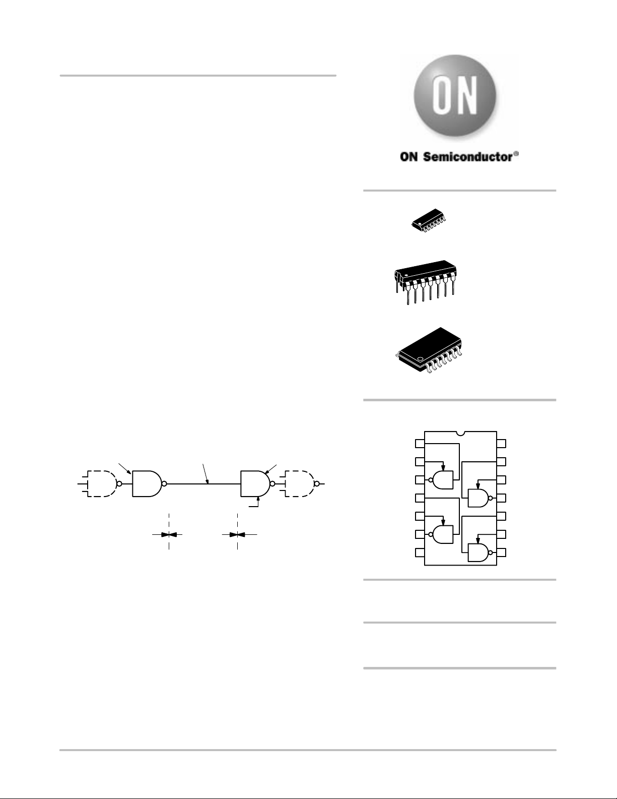
MC1489, MC1489A
Quad Line EIA−232D
Receivers
The MC1489 monolithic quad line receivers are designed to
interface data terminal equipment with data communications
equipment in conformance with the specifications of EIA Standard
No. EIA−232D.
Features
• Input Resistance − 3.0 k to 7.0 k
• Input Signal Range − ± 30 V
• Input Threshold Hysteresis Built In
• Response Control
a) Logic Threshold Shifting
b) Input Noise Filtering
• Pb−Free Packages are Available
14
14
http://onsemi.com
14
1
1
1
SOIC−14
D SUFFIX
CASE 751A
PDIP−14
P SUFFIX
CASE 646
SOEIAJ−14
M SUFFIX
CASE 965
Line Driver
MC1488
MDTL Logic Input
Interconnecting
Cable
Interconnecting
Cable
MDTL Logic Output
Figure 1. Simplified Application
Line Receiver
MC1489
1
PIN CONNECTIONS
Input A
Response
Control A
Output A
Input B
Response
Control B
Output B
Ground
1
2
3
4
5
6
7
14
13
12
11
10
9
8
V
CC
Input D
Response
Control D
Output D
Input C
Response
Control C
Output C
ORDERING INFORMATION
See detailed ordering and shipping information in the package
dimensions section on page 8 of this data sheet.
DEVICE MARKING INFORMATION
See general marking information in the device marking
section on page 8 of this data sheet.
Semiconductor Components Industries, LLC, 2004
April, 2004 − Rev. 8
*For additional information on our Pb−Free strategy
and soldering details, please download the
ON Semiconductor Soldering and Mounting
Techniques Reference Manual, SOLDERRM/D.
1 Publication Order Number:
MC1489/D
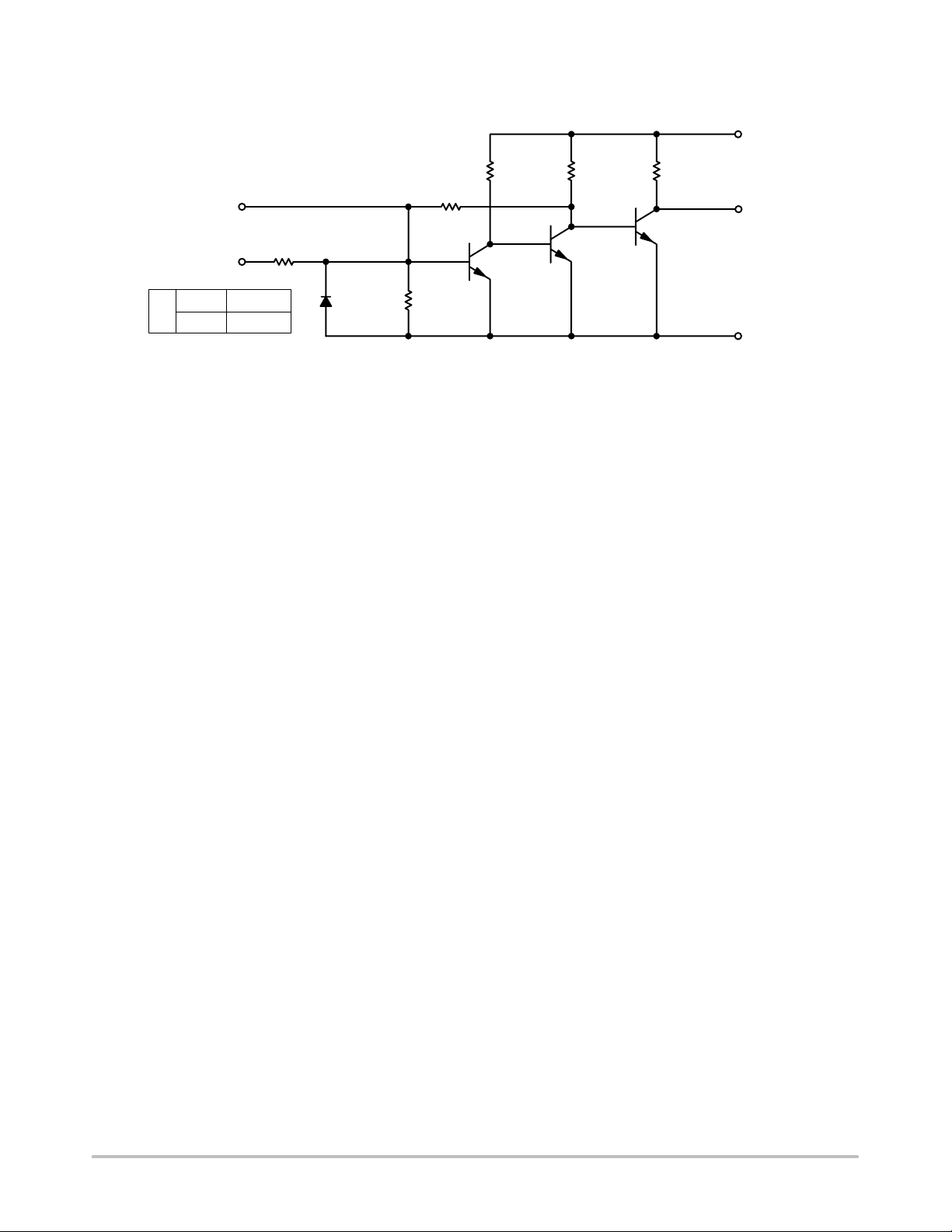
MC1489, MC1489A
14
V
CC
Response Control 2
Input 1
MC1489 MC1489A
RF6.7 k 1.6 k
3.8 k
10 k
9.0 k
R
F
5.0 k
Figure 2. Representative Schematic Diagram
(1/4 of Circuit Shown)
1.7 k
3 Output
7 GND
http://onsemi.com
2
MC1489, MC1489A
MAXIMUM RATINGS (T
Power Supply Voltage V
Input Voltage Range V
Output Load Current I
Power Dissipation (Package Limitation, SOIC−14 and Plastic Dual In−Line Package)
Derate above T
Operating Ambient Temperature Range T
Storage Temperature Range T
A
= + 25°C, unless otherwise noted)
A
= + 25°C
Rating
Symbol Value Unit
CC
IR
L
P
D
1/
JA
A
stg
10 Vdc
± 30 Vdc
20 mA
1000
6.7
mW
mW/°C
0 to + 75 °C
− 65 to + 175 °C
Maximum ratings are those values beyond which device damage can occur. Maximum ratings applied to the device are individual stress limit
values (not normal operating conditions) and are not valid simultaneously . If these limits are exceeded, device functional operation is not implied,
damage may occur and reliability may be affected.
ELECTRICAL CHARACTERISTICS (Response control pin is open.) (V
Characteristics
Positive Input Current (VIH = + 25 Vdc)
Negative Input Current (VIH = − 25 Vdc)
Input Turn−On Threshold Voltage
(T
= + 25°C, VOL 0.45 V) MC1489
A
Input Turn−Off Threshold Voltage
= + 25°C, VOH 2.5 V, IL = − 0.5 mA) MC1489
(T
A
Output Voltage High (VIH = 0.75 V, IL = − 0.5 mA)
(Input Open Circuit, I
Output Voltage Low (VIL = 3.0 V, IL = 10 mA) V
Output Short−Circuit Current I
Power Supply Current (All Gates “on,” I
= 0 mA, VIH = + 5.0 Vdc) I
out
Power Consumption (VIH = + 5.0 Vdc) P
SWITCHING CHARACTERISTICS (V
= 5.0 Vdc ± 1%, TA = + 25°C, See Figure 3.)
CC
Propagation Delay Time
Rise Time (RL = 3.9 k) t
Propagation Delay Time (RL = 390 k) t
Fall Time (RL = 390 k) t
= + 3.0 Vdc)
(V
IH
(V
= − 3.0 Vdc)
IH
MC1489A
MC1489A
= − 0.5 mA)
L
(RL = 3.9 k) t
= + 5.0 V dc ± 10%, TA = 0 to + 75°C, unless otherwise noted)
CC
Symbol Min Typ Max Unit
V
V
V
PLH
TLH
PHL
THL
I
I
IH
IL
IH
IL
OH
OL
OS
CC
C
3.6
0.43
− 3.6
− 0.43
1.0
1.75
0.75
0.75
2.5
2.5
−
−
−
−
−
1.95
−
0.8
4.0
4.0
8.3
−
− 8.3
−
1.5
2.25
1.25
1.25
5.0
5.0
− 0.2 0.45 Vdc
− − 3.0 − 4.0 mA
− 16 26 mA
− 80 130 mW
− 25 85 ns
− 120 175 ns
− 25 50 ns
− 10 20 ns
mA
mA
Vdc
Vdc
Vdc
http://onsemi.com
3

5.0 Vdc
MC1489, MC1489A
TEST CIRCUITS
R
L
All diodes
1N3064
or equivalent
V
R
E
in
3.0 V
50% 50%
E
in
E
O
t
THL
1.5 V
C
= 15 pF = total parasitic capacitance which includes
L
probe and wiring capacitances
1.5 V
t
PLH
t
TLH
Figure 3. Switching Response
C
L
t
and t
TLH
measured
10% − 90%
THL
E
o
R
C
1/4
V
in
MC1489A
Response Node
V
O
C, capacitor is for noise filtering.
R, resistor is for threshold shifting.
Figure 4. Response Control Node
http://onsemi.com
4

MC1489, MC1489A
TYPICAL CHARACTERISTICS
(VCC = 5.0 Vdc, TA = +25°C, unless otherwise noted)
10
8.0
6.0
4.0
2.0
0
−2.0
−4.0
L
I , INPUT CURRENT (mA)
−6.0
−8.0
−10
−25
6.0
5.0
4.0
3.0
2.0
1.0
O
V , OUTPUT VOLTAGE (Vdc)
0
I
I
V
I
−20 −15 −10 −5.0 5.0 15 2520
0
10
Vin, INPUT VOLTAGE (V)
Figure 5. Input Current
V
in
R
R
5.0 k
V
5.0 V
R
T
T
th
V
V
IHL
ILH
1.0 2.00 4.0−2.0 −1.0−3.0
, INPUT VOLTAGE (V)
V
I
11 k
V
th
−5.0 V
3.0
T
6.0
5.0
4.0
3.0
2.0
R
5.0 k
V
th
5.0 V
R
R
T
13 k
5.0 V
T
T
V
th
R
11 k
V
T
th
−5.0 V
V
I
E
O
R
T
V
th
1.0
O
V , OUTPUT VOLTAGE (Vdc)
0
V
V
ILH
IHL
3.02.01.00−2.0 −1.0−3.0
, INPUT VOLTAGE (V)
V
I
Figure 6. MC1489 Input Threshold
Voltage Adjustment
2.4
2.2
MC1489 V
MC1489 V
MC1489A V
IH
IL
MC1489A V
IH
IL
+120+600−60
E
O
2.0
1.8
1.6
R
T
V
th
1.4
1.2
1.0
0.8
0.6
0.4
0.2
IH
V , INPUT THRESHOLD VOLTAGE (Vdc)
0
T, TEMPERATURE (°C)
Figure 7. MC1489A Input Threshold
Voltage Adjustment
2.0
VIH MC1489A
1.0
VIH MC1489
VIL MC1489
VIL MC1489A
INPUT THRESHOLD VOLTAGE (Vdc)
0
3.0
VCC, POWER SUPPLY VOLTAGE (V)
Figure 9. Input Threshold versus
Power Supply Voltage
Figure 8. Input Threshold Voltage
versus Temperature
4.0 5.0 6.0
http://onsemi.com
5

MC1489, MC1489A
APPLICATIONS INFORMATION
General Information
The Electronic Industries Association (EIA) has released
the EIA−232D specification detailing the requirements for
the interface between data processing equipment and data
communications equipment. This standard specifies not
only the number and type of interface leads, but also the
voltage levels to be used. The MC1488 quad driver and its
companion circuit, the MC1489 quad receiver, provide a
complete interface system between DTL or TTL logic levels
and the EIA−232D defined levels. The EIA−232D
requirements as applied to receivers are discussed herein.
The required input impedance is defined as between
3000 and 7000 for input voltages between 3.0 and 25 V
in magnitude; and any voltage on the receiver input in an
open circuit condition must be less than 2.0 V in magnitude.
The MC1489 circuits meet these requirements with a
maximum open circuit voltage of one V
The receiver shall detect a voltage between − 3.0 and
−25 V as a Logic “1” and inputs between 3.0 and 25 V as a
Logic “0.” On some interchange leads, an open circuit of
power “OFF” condition (300 or more to ground) shall be
decoded as an “OFF” condition or Logic “1.” For this
reason, the input hysteresis thresholds of the MC1489
circuits are all above ground. Thus an open or grounded
input will cause the same output as a negative or Logic “1”
input.
Device Characteristics
The MC1489 interface receivers have internal feedback
from the second stage to the input stage providing input
hysteresis for noise rejection. The MC1489 input has typical
BE
.
turn−on voltage of 1.25 V and turn−off of 1.0 V for a typical
hysteresis of 250 mV. The MC1489A has typical turn−on of
1.95 V and turn−off of 0.8 V for typically 1.15 V of
hysteresis.
Each receiver section has an external response control
node in addition to the input and output pins, thereby
allowing the designer to vary the input threshold voltage
levels. A resistor can be connected between this node and an
external power supply. Figures 4, 6 and 7 illustrate the input
threshold voltage shift possible through this technique.
This response node can also be used for the filtering of
high frequency, high energy noise pulses. Figures 10 and 11
show typical noise pulse rejection for external capacitors of
various sizes.
These two operations on the response node can be
combined or used individually for many combinations of
interfacing applications. The MC1489 circuits are
particularly useful for interfacing between MOS circuits and
MDTL/MTTL logic systems. In this application, the input
threshold voltages are adjusted (with the appropriate supply
and resistor values) to fall in the center of the MOS voltage
logic levels (see Figure 12).
The response node may also be used as the receiver input
as long as the designer realizes that he may not drive this
node with a low impedance source to a voltage greater than
one diode above ground or less than one diode below
ground. This feature is demonstrated in Figure 13 where two
receivers are slaved to the same line that must still meet the
EIA−232D impedance requirement.
6
MC1489
5
4
3
in
E , AMPLITUDE (V)
2
1
Figure 10. Typical Turn On Threshold versus
Capacitance from Response Control Pin to GND
10 pF
100 pF
300 pF
PW, INPUT PULSE WIDTH (ns)
500 pF
6
5
4
3
in
E , AMPLITUDE (V)
2
10,000100010010
http://onsemi.com
1
6
MC1489A
12 pF
Figure 11. Typical Turn On Threshold versus
Capacitance from Response Control Pin to GND
100 pF 300 pF
PW, INPUT PULSE WIDTH (ns)
500 pF
10,000100010010

MC1489, MC1489A
+5.0 Vdc
R
MOS
Logic
−V
−V
DD
GG
MC1489
+5.0 Vdc
DTL or TTL
+5.0 Vdc
Figure 12. Typical Translator Application − MOS to DTL or TTL
V
CC
Response−Control Pin
Input
8.0 k
1/2 MC1489
Output
V
CC
Input
Response−Control Pin
8.0 k
Output
Figure 13. Typical Paralleling of Two MC1489, A Receivers to Meet EIA−232D
http://onsemi.com
7

MC1489, MC1489A
SO C
SO J
ORDERING INFORMATION
Device Package Operating Temperature Range Shipping
MC1489D 55 Units/Rail
MC1489DR2
MC1489AD
MC1489ADG
MC1489ADR2
MC1489ADR2G
MC1489P
MC1489PG
MC1489AP
MC1489M 50 Units/Rail
MC1489MEL
MC1489AM
MC1489AM
MC1489AMEL
MC1489AMEL
SOIC−14
SOIC−14
(Pb−Free)
SOIC−14
SOIC−14
(Pb−Free)
PDIP−14
PDIP−14
(Pb−Free)
PDIP−14
SOEIAJ−14
SOEIAJ−14
(Pb−Free)
SOEIAJ−14
SOEIAJ−14
(Pb−Free)
TA = 0 to +75°C
TA = 0 to +75°C
TA = 0 to +75°C
2500 Tape & Reel
55 Units/Rail
55 Units/Rail
2500 Tape & Reel
2500 Tape & Reel
25 Units/Rail
25 Units/Rail
25 Units/Rail
2000 Tape & Reel
50 Units/Rail
50 Units/Rail
2000 Tape & Reel
2000 Tape & Reel
14
MC1489AD
AWLYWW
1
SOIC−14
D SUFFIX
CASE 751A
14
1
MC1489D
AWLYWW
MARKING DIAGRAMS
14
SOEIAJ−14
M SUFFIX
CASE 965
MC1489A
ALYW
MC1489AP
AWLYYWW
1
MC1489
ALYW
PDIP−14
P SUFFIX
CASE 646
14
MC1489P
AWLYYWW
1
A = Assembly Location
WL, L = Wafer Lot
YY, Y = Year
WW, W = Work Week
http://onsemi.com
8

−T−
SEATING
PLANE
−A−
14 8
G
D 14 PL
0.25 (0.010) A
MC1489, MC1489A
PACKAGE DIMENSIONS
SOIC−14
D SUFFIX
CASE 751A−03
ISSUE F
NOTES:
1. DIMENSIONING AND TOLERANCING PER ANSI
Y14.5M, 1982.
2. CONTROLLING DIMENSION: MILLIMETER.
3. DIMENSIONS A AND B DO NOT INCLUDE
MOLD PROTRUSION.
−B−
P
7 PL
M
71
0.25 (0.010) B
C
X 45
R
K
M
S
B
T
S
M
M
F
J
4. MAXIMUM MOLD PROTRUSION 0.15 (0.006)
PER SIDE.
5. DIMENSION D DOES NOT INCLUDE DAMBAR
PROTRUSION. ALLOWABLE DAMBAR
PROTRUSION SHALL BE 0.127 (0.005) TOTAL
IN EXCESS OF THE D DIMENSION AT
MAXIMUM MATERIAL CONDITION.
DIM MIN MAX MIN MAX
A 8.55 8.75 0.337 0.344
B 3.80 4.00 0.150 0.157
C 1.35 1.75 0.054 0.068
D 0.35 0.49 0.014 0.019
F 0.40 1.25 0.016 0.049
G 1.27 BSC 0.050 BSC
J 0.19 0.25 0.008 0.009
K 0.10 0.25 0.004 0.009
M 0 7 0 7
P 5.80 6.20 0.228 0.244
R 0.25 0.50 0.010 0.019
INCHESMILLIMETERS
−T−
SEATING
PLANE
14 8
17
N
HG
PDIP−14
P SUFFIX
CASE 646−06
ISSUE M
NOTES:
1. DIMENSIONING AND TOLERANCING PER ANSI
Y14.5M, 1982.
B
A
F
L
C
D
14 PL
0.13 (0.005)
K
J
M
M
2. CONTROLLING DIMENSION: INCH.
3. DIMENSION L TO CENTER OF LEADS WHEN
FORMED PARALLEL.
4. DIMENSION B DOES NOT INCLUDE MOLD FLASH.
5. ROUNDED CORNERS OPTIONAL.
DIM MIN MAX MIN MAX
A 0.715 0.770 18.16 18.80
B 0.240 0.260 6.10 6.60
C 0.145 0.185 3.69 4.69
D 0.015 0.021 0.38 0.53
F 0.040 0.070 1.02 1.78
G 0.100 BSC 2.54 BSC
H 0.052 0.095 1.32 2.41
J 0.008 0.015 0.20 0.38
K 0.115 0.135 2.92 3.43
L
0.290 0.310 7.37 7.87
M −−− 10 −−− 10
N 0.015 0.039 0.38 1.01
MILLIMETERSINCHES
http://onsemi.com
9

14 8
1
Z
D
e
b
0.13 (0.005)
M
E
7
A
0.10 (0.004)
H
A
1
E
VIEW P
MC1489, MC1489A
PACKAGE DIMENSIONS
SOEIAJ−14
M SUFFIX
CASE 965−01
ISSUE O
L
E
Q
1
M
L
DETAIL P
NOTES:
1. DIMENSIONING AND TOLERANCING PER ANSI
Y14.5M, 1982.
2. CONTROLLING DIMENSION: MILLIMETER.
3. DIMENSIONS D AND E DO NOT INCLUDE MOLD
FLASH OR PROTRUSIONS AND ARE MEASURED
AT THE PARTING LINE. MOLD FLASH OR
PROTRUSIONS SHALL NOT EXCEED 0.15 (0.006)
PER SIDE.
4. TERMINAL NUMBERS ARE SHOWN FOR
REFERENCE ONLY.
5. THE LEAD WIDTH DIMENSION (b) DOES NOT
INCLUDE DAMBAR PROTRUSION. ALLOWABLE
DAMBAR PROTRUSION SHALL BE 0.08 (0.003)
TOTAL IN EXCESS OF THE LEAD WIDTH
DIMENSION AT MAXIMUM MATERIAL CONDITION.
DAMBAR CANNOT BE LOCATED ON THE LOWER
RADIUS OR THE FOOT. MINIMUM SPACE
c
BETWEEN PROTRUSIONS AND ADJACENT LEAD
TO BE 0.46 ( 0.018).
MILLIMETERS
DIM MIN MAX MIN MAX
−−− 2.05 −−− 0.081
A
A
0.05 0.20 0.002 0.008
1
0.35 0.50 0.014 0.020
b
0.18 0.27 0.007 0.011
c
9.90 10.50 0.390 0.413
D
5.10 5.45 0.201 0.215
E
1.27 BSC 0.050 BSC
e
H
7.40 8.20 0.291 0.323
E
0.50 0.85 0.020 0.033
0.50
L
1.10 1.50 0.043 0.059
E
0
M
Q
0.70 0.90 0.028 0.035
1
−−− 1.42 −−− 0.056
Z
INCHES
10
10
0
ON Semiconductor and are registered trademarks of Semiconductor Components Industries, LLC (SCILLC). SCILLC reserves the right to make changes without further notice
to any products herein. SCILLC makes no warranty, representation or guarantee regarding the suitability of its products for any particular purpose, nor does SCILLC assume any liability
arising out of the application or use of any product or circuit, and specifically disclaims any and all liability, including without limitation special, consequential or incidental damages.
“Typical” parameters which may be provided in SCILLC data sheets and/or specifications can and do vary in different applications and actual performance may vary over time. All
operating parameters, including “Typicals” must be validated for each customer application by customer’s technical experts. SCILLC does not convey any license under its patent rights
nor the rights of others. SCILLC products are not designed, intended, or authorized for use as components in systems intended for surgical implant into the body, or other applications
intended to support or sustain life, or for any other application in which the failure of the SCILLC product could create a situation where personal injury or death may occur. Should
Buyer purchase or use SCILLC products for any such unintended or unauthorized application, Buyer shall indemnify and hold SCILLC and its officers, employees, subsidiaries, affiliates,
and distributors harmless against all claims, costs, damages, and expenses, and reasonable attorney fees arising out of, directly or indirectly, any claim of personal injury or death
associated with such unintended or unauthorized use, even if such claim alleges that SCILLC was negligent regarding the design or manufacture of the part. SCILLC is an Equal
Opportunity/Affirmative Action Employer. This literature is subject to all applicable copyright laws and is not for resale in any manner.
PUBLICATION ORDERING INFORMATION
LITERATURE FULFILLMENT:
Literature Distribution Center for ON Semiconductor
P.O. Box 5163, Denver, Colorado 80217 USA
Phone: 303−675−2175 or 800−344−3860 Toll Free USA/Canada
Fax: 303−675−2176 or 800−344−3867 Toll Free USA/Canada
Email: orderlit@onsemi.com
N. American Technical Support: 800−282−9855 Toll Free
USA/Canada
Japan: ON Semiconductor, Japan Customer Focus Center
2−9−1 Kamimeguro, Meguro−ku, Tokyo, Japan 153−0051
Phone: 81−3−5773−3850
http://onsemi.com
ON Semiconductor Website: http://onsemi.com
Order Literature: http://www.onsemi.com/litorder
For additional information, please contact your
local Sales Representative.
MC1489/D
10
 Loading...