


MC14536B
Programmable Timer
The MC14536B programmable timer is a 24–stage binary ripple
counter with 16 stages selectable by a binary code. Provisions for an
on–chip RC oscillator or an external clock are provided. An on–chip
monostable circuit incorporating a pulse–type output has been
included. By selecting the appropriate counter stage in conjunction
with the appropriate input clock frequency, a variety of timing can be
achieved.
0
• 24 Flip–Flop Stages — Will Count From 2
• Last 16 Stages Selectable By Four–Bit Select Code
• 8–Bypass Input Allows Bypassing of First Eight Stages
• Set and Reset Inputs
• Clock Inhibit and Oscillator Inhibit Inputs
• On–Chip RC Oscillator Provisions
• On–Chip Monostable Output Provisions
• Clock Conditioning Circuit Permits Operation With Very Long Rise
and Fall Times
• Test Mode Allows Fast Test Sequence
• Supply Voltage Range = 3.0 Vdc to 18 Vdc
• Capable of Driving Two Low–power TTL Loads or One Low–power
Schottky TTL Load Over the Rated Temperature Range
MAXIMUM RATINGS (Voltages Referenced to V
Symbol
V
DD
Vin, V
Iin, I
P
T
T
stg
T
2. Maximum Ratings are those values beyond which damage to the device
may occur.
3. Temperature Derating:
Plastic “P and D/DW” Packages: – 7.0 mW/C From 65C To 125C
This device contains protection circuitry to guard against damage due to high
static voltages or electric fields. However, precautions must be taken to avoid
applications of any voltage higher than maximum rated voltages to this
high–impedance circuit. For proper operation, V
to the range V
Unused inputs must always be tied to an appropriate logic voltage level (e.g.,
either V
DC Supply Voltage Range –0.5 to +18.0 V
Input or Output Voltage Range
out
Input or Output Current
out
Power Dissipation,
D
Operating Temperature Range –55 to +125 °C
A
Storage Temperature Range –65 to +150 °C
Lead Temperature
L
SS
or VDD). Unused outputs must be left open.
SS
Parameter Value Unit
(DC or Transient)
(DC or Transient) per Pin
per Package (Note 3.)
(8–Second Soldering)
and V
(Vin or V
) VDD.
out
in
24
to 2
) (Note 2.)
SS
–0.5 to VDD + 0.5 V
±10 mA
500 mW
260 °C
should be constrained
out
http://onsemi.com
MARKING
DIAGRAMS
16
PDIP–16
P SUFFIX
CASE 648
SOIC–16
DW SUFFIX
CASE 751G
SOEIAJ–16
F SUFFIX
CASE 966
A = Assembly Location
WL, L = Wafer Lot
YY, Y = Year
WW, W = Work Week
MC14536BCP
AWLYYWW
1
16
14536B
AWLYYWW
1
16
MC14536B
ALYW
1
ORDERING INFORMATION
Device Package Shipping
MC14536BCP PDIP–16 2000/Box
MC14536BDW SOIC–16 47/Rail
MC14536BDWR2 SOIC–16 1000/Tape & Reel
MC14536BF SOEIAJ–16 See Note 1.
1. For ordering information on the EIAJ version of
the SOIC packages, please contact your local
ON Semiconductor representative.
Semiconductor Components Industries, LLC, 2001
February, 2001 – Rev. 7
1 Publication Order Number:
MC14536B/D

MC14536B
OSC. INHIBIT14
IN
1
3
OUT
SET
RESET
IN 1
OUT 1
OUT 2
8-BYPASS
CLOCK INH
V
1
2
3
4
6
7
8
SS
16
15
14
13
125
11
10
9
V
DD
MONO-IN
OSC INH
DECODE
D
C
B
A
Figure 1. Pin Assignment
A9
B10
C11
D12
8 BYPASSSETRESETCLOCK INH.
STAGES 9 THRU 24
Q24Q23Q22Q21Q20Q19Q18Q17Q16Q15Q14Q13Q12Q11Q10Q
9
DECODER
MONOSTABLE
MULTIVIBRATOR
13MONO-IN15
DECODE
OUT
7216
STAGES
1 THRU 8
4
5
OUT
1
2
V
= PIN 16
DD
V
= PIN 8
SS
Figure 2. Block Diagram
http://onsemi.com
2

MC14536B
ELECTRICAL CHARACTERISTICS (Voltages Referenced to V
SS
)
– 55C 25C 125C
Typ
(Note 4.)
0
0
0
5.0
10
15
2.25
4.50
6.75
2.75
5.50
8.25
– 1.7
– 0.36
– 0.9
– 3.5
– 4.2
– 0.88
– 2.25
– 8.8
0.88
2.25
8.8
0.010
0.020
0.030
Max Min Max
0.05
0.05
0.05
—
—
—
1.5
3.0
4.0
—
—
—
—
—
—
—
—
—
—
—
—
—
—
5.0
10
20
DD
DD
DD
—
—
—
4.95
9.95
14.95
—
—
—
3.5
7.0
11
– 0.7
– 0.14
– 0.35
– 1.1
– 1.7
– 0.36
– 0.9
– 2.4
0.36
0.9
2.4
—
—
—
0.05
0.05
0.05
Characteristic Symbol
Output Voltage “0” Level
V
= VDD or 0
in
“1” Level
V
= 0 or V
in
DD
Input Voltage “0” Level
(V
= 4.5 or 0.5 Vdc)
O
= 9.0 or 1.0 Vdc)
(V
O
(V
= 13.5 or 1.5 Vdc)
O
“1” Level
(V
= 0.5 or 4.5 Vdc)
O
= 1.0 or 9.0 Vdc)
(V
O
(V
= 1.5 or 13.5 Vdc)
O
Output Drive Current
(V
= 2.5 Vdc) Source
OH
= 4.6 Vdc) Pins 4 & 5
(V
OH
(V
= 9.5 Vdc)
OH
(V
= 13.5 Vdc)
OH
(VOH = 2.5 Vdc) Source
(V
= 4.6 Vdc) Pin 13
OH
= 9.5 Vdc)
(V
OH
(V
= 13.5 Vdc)
OH
(VOL = 0.4 Vdc) Sink
(V
= 0.5 Vdc)
OL
(V
= 1.5 Vdc)
OL
Input Current I
Input Capacitance
(V
= 0)
in
Quiescent Current
(Per Package)
Total Supply Current (Note 5., 6.)
(Dynamic plus Quiescent,
Per Package)
(C
= 50 pF on all outputs, all
L
V
DD
Vdc
V
OL
5.0
10
15
V
OH
5.0
10
15
V
IL
5.0
10
15
V
IH
5.0
10
15
I
OH
5.0
5.0
10
15
5.0
5.0
10
15
I
OL
5.0
10
15
in
C
in
I
DD
15 — ±0.1 — ±0.00001 ±0.1 — ±1.0 µAdc
— — — — 5.0 7.5 — — pF
5.0
10
15
I
T
5.0
10
15
Min Max Min
—
—
—
4.95
9.95
14.95
—
—
—
3.5
7.0
11
– 1.2
– 0.25
– 0.62
– 1.8
– 3.0
– 0.64
– 1.6
– 4.2
0.64
1.6
4.2
—
—
—
0.05
0.05
0.05
—
—
—
1.5
3.0
4.0
—
—
—
—
—
—
—
—
—
—
—
—
—
—
5.0
10
20
14.95
– 0.25
– 2.4
– 0.51
—
—
—
4.95
9.95
—
—
—
3.5
7.0
11
– 1.0
– 0.5
– 1.5
– 1.3
– 3.4
0.51
1.3
3.4
—
—
—
IT = (1.50 µA/kHz) f + I
IT = (2.30 µA/kHz) f + I
IT = (3.55 µA/kHz) f + I
buffers switching)
4. Data labelled “Typ” is not to be used for design purposes but is intended as an indication of the IC’s potential performance.
5. The formulas given are for the typical characteristics only at 25C.
6. To calculate total supply current at loads other than 50 pF:
IT(CL) = IT(50 pF) + (CL – 50) Vfk
where: I
is in µA (per package), CL in pF, V = (VDD – VSS) in volts, f in kHz is input frequency, and k = 0.003.
T
—
—
—
1.5
3.0
4.0
—
—
—
—
—
—
—
—
—
—
—
—
—
—
150
300
600
Unit
Vdc
Vdc
Vdc
Vdc
mAdc
mAdc
mAdc
µAdc
µAdc
http://onsemi.com
3

MC14536B
SWITCHING CHARACTERISTICS (Note 7.) (C
Characteristic Symbol V
= 50 pF, T
L
= 25C)
A
DD
Min Typ
Max Unit
(Note 8.)
Output Rise and Fall Time (Pin 13)
t
, t
TLH
t
TLH
t
TLH
= (1.5 ns/pF) CL + 25 ns
THL
, t
= (0.75 ns/pF) CL + 12.5 ns
THL
, t
= (0.55 ns/pF) CL + 9.5 ns
THL
Propagation Delay Time
Clock to Q1, 8–Bypass (Pin 6) High
, t
t
PLH
t
PLH
t
PLH
= (1.7 ns/pF) CL + 1715 ns
PHL
, t
= (0.66 ns/pF) CL + 617 ns
PHL
, t
= (0.5 ns/pF) CL + 425 ns
PHL
Clock to Q1, 8–Bypass (Pin 6) Low
t
, t
PLH
t
PLH
t
PLH
= (1.7 ns/pF) CL + 3715 ns
PHL
, t
= (0.66 ns/pF) CL + 1467 ns
PHL
, t
= (0.5 ns/pF) CL + 1075 ns
PHL
Clock to Q16
t
, t
PHL
t
PHL
t
PHL
Reset to Q
t
PHL
t
PHL
t
PHL
= (1.7 ns/pF) CL + 6915 ns
PLH
, t
= (0.66 ns/pF) CL + 2967 ns
PLH
, t
= (0.5 ns/pF) CL + 2175 ns
PLH
n
= (1.7 ns/pF) CL + 1415 ns
= (0.66 ns/pF) CL + 567 ns
= (0.5 ns/pF) CL + 425 ns
Clock Pulse Width t
Clock Pulse Frequency
(50% Duty Cycle)
Clock Rise and Fall Time t
t
TLH
t
t
PLH
t
t
PLH
t
t
PLH
t
t
TLH
t
THL
PHL
PHL
PHL
PHL
WH
f
cl
THL
,
5.0
10
15
—
—
—
100
50
40
200
100
80
,
5.0
10
15
—
—
—
1800
650
450
3600
1300
1000
,
5.0
10
15
—
—
—
3.8
1.5
1.1
7.6
3.0
2.3
,
5.0
10
15
5.0
10
15
5.0
10
15
5.0
10
15
,
5.0
10
—
—
—
—
—
—
600
200
170
—
—
—
7.0
3.0
2.2
1500
600
450
300
100
85
1.2
3.0
5.0
No Limit
14
6.0
4.5
3000
1200
900
—
—
—
0.4
1.5
2.0
15
Reset Pulse Width t
WH
5.0
10
15
1000
400
300
500
200
150
—
—
—
7. The formulas given are for the typical characteristics only at 25C.
8. Data labelled “Typ” is not to be used for design purposes but is intended as an indication of the IC’s potential performance.
ns
ns
µs
µs
ns
ns
MHz
—
ns
http://onsemi.com
4

MC14536B
PIN DESCRIPTIONS
INPUTS
SET (Pin 1) — A high on Set asynchronously forces
Decode Out to a high level. This is accomplished by setting
an output conditioning latch to a high level while at the same
time resetting the 24 flip–flop stages. After Set goes low
(inactive), the occurrence of the first negative clock
transition on IN
causes Decode Out to go low. The
1
counter’s flip–flop stages begin counting on the second
negative clock transition of IN
. When Set is high, the
1
on–chip RC oscillator is disabled. This allows for very
low–power standby operation.
RESET (Pin 2) — A high on Reset asynchronously
forces Decode Out to a low level; all 24 flip–flop stages are
also reset to a low level. Like the Set input, Reset disables
the on–chip RC oscillator for standby operation.
IN
(Pin 3) — The device’s internal counters advance on
1
the negative–going edge of this input. IN
may be used as an
1
external clock input or used in conjunction with OUT1 and
OUT2 to form an RC oscillator. When an external clock is
used, both OU T1 and OU T2 may be left unconnected or
used to drive 1 LSTTL or several CMOS loads.
8–BYPASS (Pin 6) — A high on this input causes the first
8 flip–flop stages to be bypassed. This device essentially
becomes a 16–stage counter with all 16 stages selectable.
Selection is accomplished by the A, B, C, and D inputs. (See
the truth tables.)
CLOCK INHIBIT (Pin 7) — A high on this input
disconnects the first counter stage from the clocking source.
This holds the present count and inhibits further counting.
However, the clocking source may continue to run.
Therefore, when Clock Inhibit is brought low, no oscillator
start–up time is required. When Clock Inhibit is low, the
counter will start counting on the occurrence of the first
negative edge of the clocking source at IN
.
1
OSC INHIBIT (Pin 14) — A high level on this pin stops
the RC oscillator which allows for very low–power standby
operation. May also be used, in conjunction with an external
clock, with essentially the same results as the Clock Inhibit
input.
MONO–IN (Pin 15) — Used as the timing pin for the
on–chip monostable multivibrator. If the Mono–In input is
connected to V
, the monostable circuit is disabled, and
SS
Decode Out is directly connected to the selected Q output.
The monostable circuit is enabled if a resistor is connected
between Mono–In and V
. This resistor and the device’s
DD
internal capacitance will determine the minimum output
pulse widths. With the addition of an external capacitor to
V
, the pulse width range may be extended. For reliable
SS
operation the resistor value should be limited to the range of
5 kΩ to 100 kΩ and the capacitor value should be limited to
a maximum of 1000 pf. (See figures 3, 4, 5, and 10).
A, B, C, D (Pins 9, 10, 11, 12) — These inputs select the
flip–flop stage to be connected to Decode Out. (See the truth
tables.)
OUTPUTS
OUT1, OUT2 (Pin 4, 5) — Outputs used in conjunction
with IN1 to form an RC oscillator. These outputs are
buffered and may be used for 2
0
frequency division of an
external clock.
DECODE OUT (Pin 13) — Output function depends on
configuration. When the monostable circuit is disabled, this
output is a 50% duty cycle square wave during free run.
TEST MODE
The test mode configuration divides the 24 flip–flop
stages into three 8–stage sections to facilitate a fast test
sequence. The test mode is enabled when 8–Bypass, Set a nd
Reset are at a high level. (See Figure 8.)
http://onsemi.com
5

Input
Stage Selected
Stage Selected
8–Bypass D C B A
0 0 0 0 0 9
0 0 0 0 1 10
0 0 0 1 0 11
0 0 0 1 1 12
0 0 1 0 0 13
0 0 1 0 1 14
0 0 1 1 0 15
0 0 1 1 1 16
0 1 0 0 0 17
0 1 0 0 1 18
0 1 0 1 0 19
0 1 0 1 1 20
0 1 1 0 0 21
0 1 1 0 1 22
0 1 1 1 0 23
0 1 1 1 1 24
TRUTH TABLES
for Decode Out
MC14536B
8–Bypass D C B A
Input
for Decode Out
1 0 0 0 0 1
1 0 0 0 1 2
1 0 0 1 0 3
1 0 0 1 1 4
1 0 1 0 0 5
1 0 1 0 1 6
1 0 1 1 0 7
1 0 1 1 1 8
1 1 0 0 0 9
1 1 0 0 1 10
1 1 0 1 0 11
1 1 0 1 1 12
1 1 1 0 0 13
1 1 1 0 1 14
1 1 1 1 0 15
1 1 1 1 1 16
FUNCTION TABLE
Clock
In
X 1 0 0 0 0 1 1
X 0 1 0 0 0 1 0
X 0 0 1 0 — — No
X 0 0 0 1 0 1 No
0 0 0 0 X 0 1 No
1 0 0 0 Advance to
X = Don’t Care
1
Set Reset
0 0 0 0 No
0 0 0 0 Advance to
Inh
OSC
Inh
Out 1 Out 2
Decode
Out
Change
next state
Change
Change
Change
next state
http://onsemi.com
6

8-BYPASS
MC14536B
LOGIC DIAGRAM
2417
23
STAGES
18 THRU
OUT
DECODER
16
15
STAGES
10 THRU
9
6
T
C11
A9
B10
D12
DECODER
13
= PIN 8
= PIN 16
SS
DD
V
V
15
MONO-IN
2
RESET
14
OSC INHIBIT
3
8
STAGES
2 THRU 7
1
T
Q
S
R
En
C
OUT 2 5
4
OUT 1
1
IN
SET
7
CLOCK
INHIBIT
1
http://onsemi.com
7

TYPICAL RC OSCILLATOR CHARACTERISTICS
(For Circuit Diagram See Figure 11 In Application)
8.0
VDD = 15 V
4.0
0
10 V
-4.0
-8.0
FREQUENCY DEVIATION (%)
-12
= 56 kΩ,
R
TC
C = 1000 pF
-16
-55 -25 0 25 50 75 100 125
*Device Only.
RS = 0, f = 10.15 kHz @ VDD = 10 V, T
R
= 120 kΩ, f = 7.8 kHz @ V
S
T
, AMBIENT TEMPERATURE (°C)*
A
5.0 V
= 10 V, T
DD
A
Figure 1. RC Oscillator Stability Figure 2. RC Oscillator Frequency as a
MONOSTABLE CHARACTERISTICS
(For Circuit Diagram See Figure 10 In Application)
100
FORMULA FOR CALCULATING tW IN
MICROSECONDS IS AS FOLLOWS:
= 0.00247 R
t
W
WHERE R IS IN kΩ, C
µs)
10
X
• C
X
0.85
IN pF.
X
MC14536B
= 25°C
= 25°C
A
100
50
20
10
VDD = 10 V
f AS A FUNCTION
OF R
TC
(C = 1000 pF)
(R
≈ 2R
)
S
TC
5.0
f AS A FUNCTION
2.0
1.0
0.5
f, OSCILLATOR FREQUENCY (kHz)
0.2
0.1
1.0 k 10 k 100 k 1.0 M
0.0001 0.001 0.01 0.1
(R
(R
OF C
= 56 kΩ)
TC
= 120 k)
S
R
, RESISTANCE (OHMS)
TC
C, CAPACITANCE (µF)
Function of RTC and C
100
FORMULA FOR CALCULATING tW IN
MICROSECONDS IS AS FOLLOWS:
= 0.00247 R
t
W
WHERE R IS IN kΩ, C
µs)
10
• C
0.85
X
X
IN pF.
X
R
= 100 kΩ
X
50 kΩ
1.0
, PULSE WIDTH (t
W
0.1
10 kΩ
5 kΩ
, EXTERNAL CAPACITANCE (pF)
C
X
T
= 25°C
A
V
DD
= 5 V
1000100101.0
Figure 3. T ypical CX versus Pulse Width
@ VDD = 5.0 V
100
FORMULA FOR CALCULATING tW IN
R
= 100 kΩ
X
50 kΩ
1.0
, PULSE WIDTH (t
W
0.1
10 kΩ
5 kΩ
C
, EXTERNAL CAPACITANCE (pF)
X
T
V
= 25°C
A
= 10 V
DD
1000100101.0
Figure 4. Typical CX versus Pulse Width
@ VDD = 10 V
MICROSECONDS IS AS FOLLOWS:
= 0.00247 R
t
W
WHERE R IS IN kΩ, C
µs)
10
R
= 100 kΩ
X
1.0
, PULSE WIDTH (t
W
50 kΩ
10 kΩ
5 kΩ
0.1
• C
0.85
X
X
IN pF.
X
, EXTERNAL CAPACITANCE (pF)
C
X
T
A
V
DD
= 25°C
= 15 V
1000100101.0
Figure 5. T ypical CX versus Pulse Width
@ V
= 15 V
DD
http://onsemi.com
8

500 µF
MC14536B
V
DD
0.01 µF
I
D
CERAMIC
SET
RESET
PULSE
GENERATOR
20 ns
8-BYPASS
IN
1
C INH
MONO-IN
OSC INH
A
B
C
D
90%
10%
50%
DUTY CYCLE
OUT 1
OUT
DECODE
OUT
V
50%
SS
C
L
2
C
20 ns
L
C
L
PULSE
GENERATOR
Figure 6. Power Dissipation Test
Circuit and Waveform
FUNCTIONAL TEST SEQUENCE
Test function (Figure 8) has been included for the
reduction of test time required to exercise all 24 counter
stages. This test function divides the counter into three
8–stage sections and 255 counts are loaded in each of the
8–stage sections in parallel. All flip–flops are now at a “1”.
The counter is now returned to the normal 24–stages in
series configuration. One more pulse is entered into In
which will cause the counter to ripple from an all “1” state
to an all “0” state.
20 ns
50%
t
TLH
SET
RESET
8-BYPASS
IN
1
C INH
MONO-IN
OSC INH
A
B
C
DECODE
D
V
DD
OUT 1
OUT
OUT
V
SS
20 ns
IN
1
t
WL
OUT
t
PLH
2
C
L
90%
10%
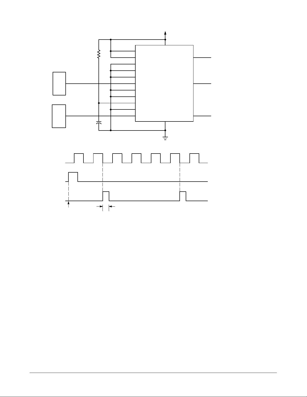
Figure 7. Switching Time Test Circuit and Waveforms
V
DD
SET
RESET
PULSE
GENERATOR
1
8-BYPASS
IN
1
C INH
MONO-IN
OSC INH
A
B
C
DECODE
D
OUT 1
OUT
OUT
V
SS
2
t
THL
t
WH
50%
t
PHL
http://onsemi.com
9
Figure 8. Functional Test Circuit

MC14536B
All 24 stages are in Reset mode
FUNCTIONAL TEST SEQUENCE
Inputs Outputs Comments
Decade Out
In
1 0 1 1 0
1 1 1 1 0 Counter is in three 8 stage sections in parallel mode.
0 1 1 1 0 First “1” to “0” transition of clock.
1
0
—
—
—
0 1 1 1 1 The 255 “1” to “0” transition.
0 0 0 0 1 Counter converted back to 24 stages in series mode.
1 0 0 0 1 In1 Switches to a “1”.
0 0 0 0 0 Counter Ripples from an all “1” state to an all “0” state.
Set Reset 8–Bypass
1
1 1 1 255 “1” to “0” transitions are clocked in the counter.
Q1 thru Q24
All 24 stages are in Reset mode.
Set and Reset must be connected together and simultaneously
go from “1” to “0”.
.
http://onsemi.com
10

PULSE
GEN.
PULSE
GEN.
CLOCK
IN
1
MC14536B
+V
16
6
8-BYPASS
9
A
10
B
11
C
12
D
2
RESET
14
OSC INH
15
MONO-IN
1
SET
7
CLOCK INH
313
IN
1
V
DD
DECODE OUT
V
SS
8
OUT 1
OUT 2
4
5
SET
CLOCK INH
DECODE OUT
POWER UP
NOTE: When power is first applied to the device, DECODE OUT can be either at a high or low state.
On the rising edge of a SET pulse the output goes high if initially at a low state. The output
remains high if initially at a high state. Because CLOCK INH is held high, the clock source
on the input pin has no effect on the output. Once CLOCK INH is taken low , the output goes
low on the first negative clock transition. The output returns high depending on the 8–BYPASS, A, B, C, and D inputs, and the clock input period. A 2
= the number of stages selected from the truth table) is obtainable at DECODE OUT. A
0
–divided output of IN1 can be obtained at OUT1 and OUT2.
2
n
frequency division (where n
Figure 9. Time Interval Configuration Using an External Clock, Set,
and Clock Inhibit Functions
(Divide–by–2 Configured)
http://onsemi.com
11
PULSE
GEN.
CLOCK
IN
MC14536B
+V
16
6
R
X
C
X
1
8-BYPASS
9
A
10
B
11
C
12
D
2
RESET
1
SET
7
CLOCK INH
15
MONO-IN
14
OSC INH
313
IN
1
V
DD
DECODE OUT
V
SS
8
OUT 1
OUT 2
4
5
RESET
*tw ≈ .00247 • RX • CX0.85
t
in µsec
DECODE OUT
*t
w
w
R
C
in kΩ
X
in pF
X
POWER UP
NOTE: When Power is first applied to the device with the RESET input going high, DECODE OUT initializes low. Bringing the
RESET input low enables the chip’s internal counters. After RESET goes low, the 2
n
/2 negative transition of the clock
input causes DECODE OUT to go high. Since the MONO–IN input is being used, the output becomes monostable. The
pulse width of the output is dependent on the external timing components. The second and all subsequent pulses occur
n
at 2
x (the clock period) intervals where n = the number of stages selected from the truth table.
Figure 10. Time Interval Configuration Using an External Clock, Reset,
and Output Monostable to Achieve a Pulse Output
(Divide–by–4 Configured)
http://onsemi.com
12

PULSE
GEN.
MC14536B
+V
R
16
6
8-BYPASS
9
A
10
B
11
C
12
D
2
RESET
14
OSC INH
15
MONO-IN
1
SET
7
CLOCK INH
313
IN
1
V
DD
DECODE OUT
V
SS
OUT 1
OUT 2
4
5
8
S
C
R
TC
RESET
OUT 1
OUT 2
1
2.3RtcC
tc
≥ R
= Hz
= Ohms
= FARADS
DECODE OUT
POWER UP
f
osc
R
s
t
w
F
R
C
NOTE: This circuit is designed to use the on–chip oscillation function. The oscillator frequency is deter-
mined by the external R and C components. When power is first applied to the device, DECODE
OUT initializes to a high state. Because this output is tied directly to the OSC INH input, the oscillator
is disabled. This puts the device in a low–current standby condition. The rising edge of the RESET
pulse will cause the output to go low . This in turn causes OSC INH to go low. However, while RESET
is high, the oscillator is still disabled (i.e.: standby condition). After RESET goes low, the output remains low for 2
n
/2 of the oscillator’s period. After the part times out, the output again goes high.
Figure 11. Time Interval Configuration Using On–Chip RC Oscillator and
Reset Input to Initiate Time Interval
(Divide–by–2 Configured)
http://onsemi.com
13

PACKAGE DIMENSIONS
PLASTIC DIP PACKAGE
–A–
916
B
18
F
H
G
D
16 PL
0.25 (0.010) T
C
S
SEATING
–T–
PLANE
K
M
A
MC14536B
PDIP–16
P SUFFIX
CASE 648–08
ISSUE R
J
M
NOTES:
1. DIMENSIONING AND TOLERANCING PER ANSI
Y14.5M, 1982.
2. CONTROLLING DIMENSION: INCH.
3. DIMENSION L TO CENTER OF LEADS WHEN
FORMED PARALLEL.
4. DIMENSION B DOES NOT INCLUDE MOLD FLASH.
5. ROUNDED CORNERS OPTIONAL.
DIM MIN MAX MIN MAX
L
M
A 0.740 0.770 18.80 19.55
B 0.250 0.270 6.35 6.85
C 0.145 0.175 3.69 4.44
D 0.015 0.021 0.39 0.53
F 0.040 0.70 1.02 1.77
G 0.100 BSC 2.54 BSC
H 0.050 BSC 1.27 BSC
J 0.008 0.015 0.21 0.38
K 0.110 0.130 2.80 3.30
L 0.295 0.305 7.50 7.74
M 0 10 0 10
S 0.020 0.040 0.51 1.01
MILLIMETERSINCHES
16 9
M
B
H8X
M
0.25
0.25 B
14X
SOIC–16
DW SUFFIX
PLASTIC SOIC PACKAGE
CASE 751G–03
ISSUE B
D
B16X
M
S
A
T
e
A
NOTES:
1. DIMENSIONS ARE IN MILLIMETERS.
2. INTERPRET DIMENSIONS AND TOLERANCES
PER ASME Y14.5M, 1994.
E
h X 45
81
B
S
A
L
A1
SEATING
PLANE
T
C
3. DIMENSIONS D AND E DO NOT INLCUDE MOLD
PROTRUSION.
4. MAXIMUM MOLD PROTRUSION 0.15 PER SIDE.
5. DIMENSION B DOES NOT INCLUDE DAMBAR
PROTRUSION. ALLOWABLE DAMBAR
PROTRUSION SHALL BE 0.13 TOTAL IN EXCESS
OF THE B DIMENSION AT MAXIMUM MATERIAL
CONDITION.
MILLIMETERS
DIM MIN MAX
A 2.35 2.65
A1 0.10 0.25
B 0.35 0.49
C 0.23 0.32
D 10.15 10.45
E 7.40 7.60
e 1.27 BSC
H 10.05 10.55
h 0.25 0.75
L 0.50 0.90
0 7
http://onsemi.com
14

16 9
1
Z
D
e
b
0.13 (0.005)
M
8
H
E
E
A
A
1
0.10 (0.004)
MC14536B
PACKAGE DIMENSIONS
SOEIAJ–16
F SUFFIX
PLASTIC EIAJ SOIC PACKAGE
CASE 966–01
ISSUE O
L
E
M
L
DETAIL P
VIEW P
NOTES:
1. DIMENSIONING AND TOLERANCING PER ANSI
Y14.5M, 1982.
2. CONTROLLING DIMENSION: MILLIMETER.
3. DIMENSIONS D AND E DO NOT INCLUDE MOLD
FLASH OR PROTRUSIONS AND ARE MEASURED
Q
1
c
AT THE PARTING LINE. MOLD FLASH OR
PROTRUSIONS SHALL NOT EXCEED 0.15 (0.006)
PER SIDE.
4. TERMINAL NUMBERS ARE SHOWN FOR
REFERENCE ONLY.
5. THE LEAD WIDTH DIMENSION (b) DOES NOT
INCLUDE DAMBAR PROTRUSION. ALLOWABLE
DAMBAR PROTRUSION SHALL BE 0.08 (0.003)
TOTAL IN EXCESS OF THE LEAD WIDTH
DIMENSION AT MAXIMUM MATERIAL CONDITION.
DAMBAR CANNOT BE LOCATED ON THE LOWER
RADIUS OR THE FOOT. MINIMUM SPACE
BETWEEN PROTRUSIONS AND ADJACENT LEAD
TO BE 0.46 ( 0.018).
MILLIMETERS
DIM MIN MAX MIN MAX
--- 2.05 --- 0.081
A
A
0.05 0.20 0.002 0.008
1
0.35 0.50 0.014 0.020
b
0.18 0.27 0.007 0.011
c
9.90 10.50 0.390 0.413
D
5.10 5.45 0.201 0.215
E
1.27 BSC 0.050 BSC
e
H
7.40 8.20 0.291 0.323
E
0.50 0.85 0.020 0.033
L
L
1.10 1.50 0.043 0.059
E
0
M
Q
0.70 0.90 0.028 0.035
1
--- 0.78 --- 0.031
Z
INCHES
10
10
0
http://onsemi.com
15

MC14536B
ON Semiconductor and are trademarks of Semiconductor Components Industries, LLC (SCILLC). SCILLC reserves the right to make changes
without further notice to any products herein. SCILLC makes no warranty, representation or guarantee regarding the suitability of its products for any particular
purpose, nor does SCILLC assume any liability arising out of the application or use of any product or circuit, and specifically disclaims any and all liability,
including without limitation special, consequential or incidental damages. “Typical” parameters which may be provided in SCILLC data sheets and/or
specifications can and do vary in different applications and actual performance may vary over time. All operating parameters, including “Typicals” must be
validated for each customer application by customer’s technical experts. SCILLC does not convey any license under its patent rights nor the rights of others.
SCILLC products are not designed, intended, or authorized for use as components in systems intended for surgical implant into the body, or other applications
intended to support or sustain life, or for any other application in which the failure of the SCILLC product could create a situation where personal injury or
death may occur. Should Buyer purchase or use SCILLC products for any such unintended or unauthorized application, Buyer shall indemnify and hold
SCILLC and its officers, employees, subsidiaries, affiliates, and distributors harmless against all claims, costs, damages, and expenses, and reasonable
attorney fees arising out of, directly or indirectly, any claim of personal injury or death associated with such unintended or unauthorized use, even if such claim
alleges that SCILLC was negligent regarding the design or manufacture of the part. SCILLC is an Equal Opportunity/Affirmative Action Employer.
PUBLICATION ORDERING INFORMATION
NORTH AMERICA Literature Fulfillment:
Literature Distribution Center for ON Semiconductor
P.O. Box 5163, Denver, Colorado 80217 USA
Phone: 303–675–2175 or 800–344–3860 Toll Free USA/Canada
Fax: 303–675–2176 or 800–344–3867 Toll Free USA/Canada
Email: ONlit@hibbertco.com
Fax Response Line: 303–675–2167 or 800–344–3810 Toll Free USA/Canada
N. American Technical Support: 800–282–9855 Toll Free USA/Canada
EUROPE: LDC for ON Semiconductor – European Support
German Phone: (+1) 303–308–7140 (Mon–Fri 2:30pm to 7:00pm CET)
Email: ONlit–german@hibbertco.com
French Phone: (+1) 303–308–7141 (Mon–Fri 2:00pm to 7:00pm CET)
Email: ONlit–french@hibbertco.com
English Phone: (+1) 303–308–7142 (Mon–Fri 12:00pm to 5:00pm GMT)
Email: ONlit@hibbertco.com
EUROPEAN TOLL–FREE ACCESS*: 00–800–4422–3781
*Available from Germany, France, Italy, UK, Ireland
CENTRAL/SOUTH AMERICA:
Spanish Phone: 303–308–7143 (Mon–Fri 8:00am to 5:00pm MST)
Email: ONlit–spanish@hibbertco.com
Toll–Free from Mexico: Dial 01–800–288–2872 for Access –
then Dial 866–297–9322
ASIA/PACIFIC: LDC for ON Semiconductor – Asia Support
Phone: 303–675–2121 (Tue–Fri 9:00am to 1:00pm, Hong Kong Time)
Toll Free from Hong Kong & Singapore:
001–800–4422–3781
Email: ONlit–asia@hibbertco.com
JAPAN: ON Semiconductor, Japan Customer Focus Center
4–32–1 Nishi–Gotanda, Shinagawa–ku, Tokyo, Japan 141–0031
Phone: 81–3–5740–2700
Email: r14525@onsemi.com
ON Semiconductor Website: http://onsemi.com
For additional information, please contact your local
Sales Representative.
http://onsemi.com
16
MC14536B/D
 Loading...