

MC14516B
Binary Up/Down Counter
The MC14516B synchronous up/down binary counter is
constructed with MOS P–channel and N–channel enhancement mode
devices in a monolithic structure.
This counter can be preset by applying the desired value, in binary,
to the Preset inputs (P0, P1, P2, P3) and then bringing the Preset
Enable (PE) high. The direction of counting is controlled by applying
a high (for up counting) or a low (for down counting) to the
UP/DOWN input. The state of the counter changes on the positive
transition of the clock input.
Cascading can be accomplished by connecting the Carry Out
Carry In of the next stage while clocking each counter in parallel. The
outputs (Q0, Q1, Q2, Q3) can be reset to a low state by applying a high
to the reset (R) pin.
This CMOS counter finds primary use in up/down and difference
counting. Other applications include: (1) Frequency synthesizer
applications where low power dissipation and/or high noise immunity
is desired, (2) Analog–to–digital and digital–to–analog conversions,
and (3) Magnitude and sign generation.
• Diode Protection on All Inputs
• Supply Voltage Range = 3.0 Vdc to 18 Vdc
• Internally Synchronous for High Speed
• Logic Edge–Clocked Design — Count Occurs on Positive Going
Edge of Clock
• Single Pin Reset
• Asynchronous Preset Enable Operation
• Capable of Driving Two Low–Power TTL Loads or One Low–Power
Schottky Load Over the Rated Temperature Range
to the
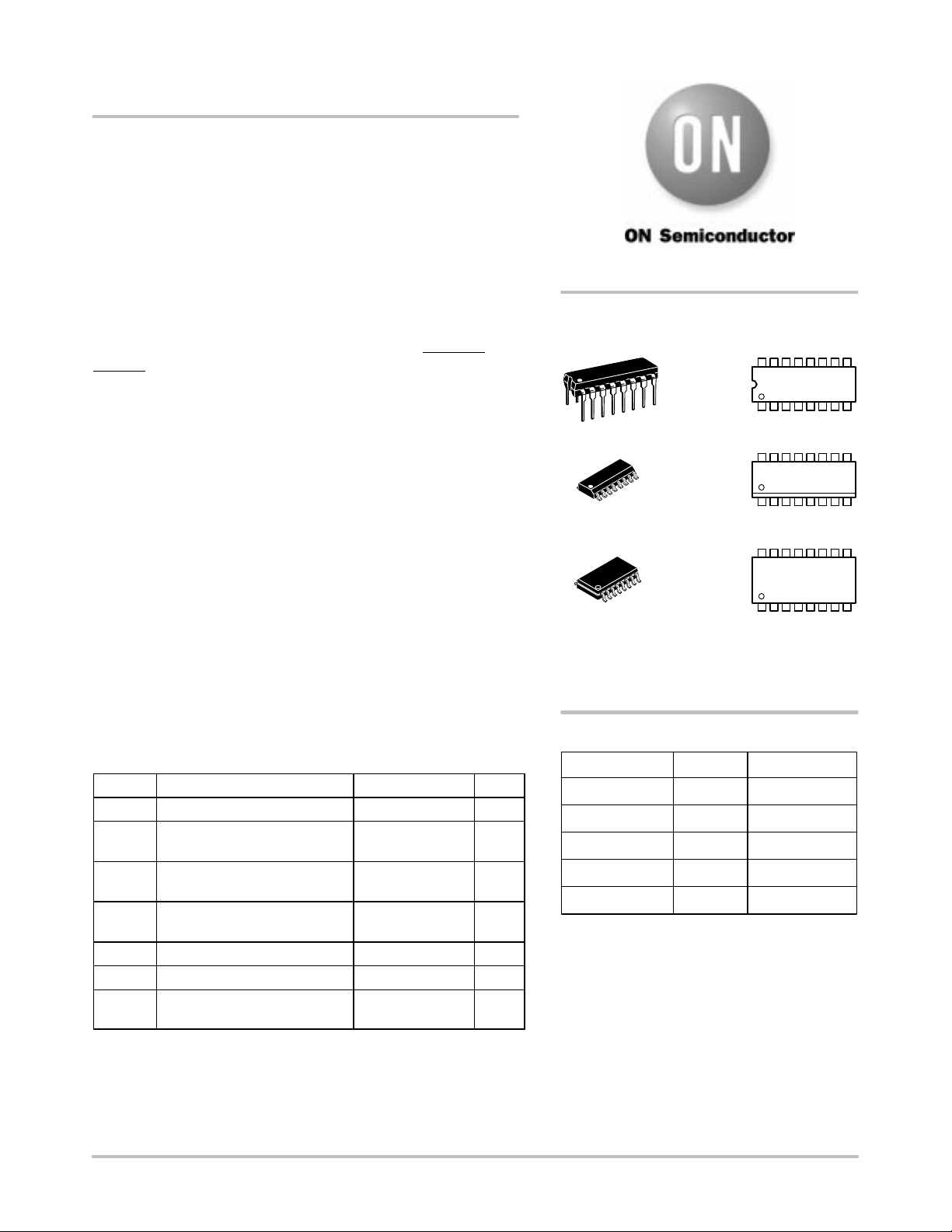
http://onsemi.com
MARKING
DIAGRAMS
16
PDIP–16
P SUFFIX
CASE 648
SOIC–16
D SUFFIX
CASE 751B
SOEIAJ–16
F SUFFIX
CASE 966
A = Assembly Location
WL, L = Wafer Lot
YY, Y = Year
WW, W = Work Week
MC14516BCP
AWLYYWW
1
16
AWLYWW
1
16
MC14516B
1
14516B
ALYW
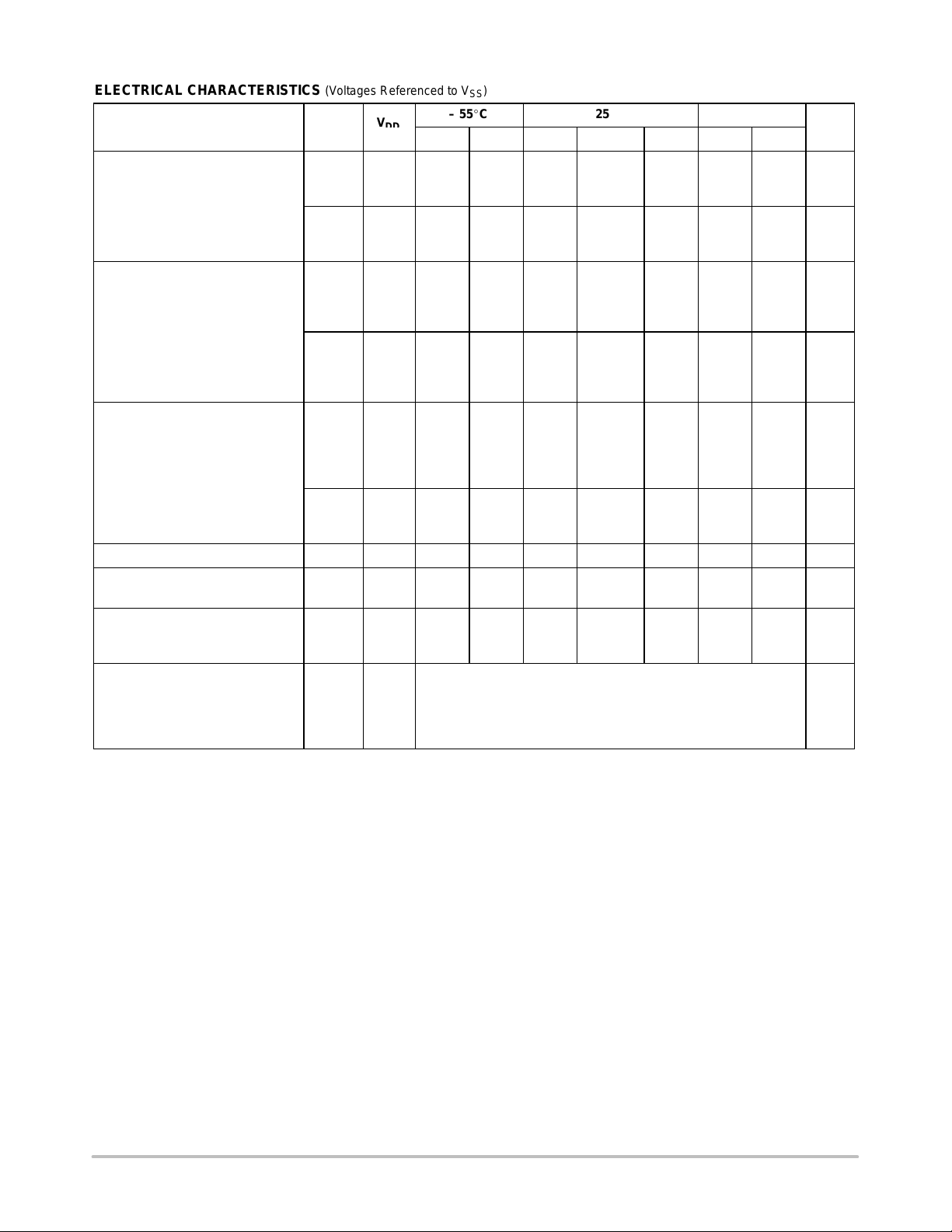
MAXIMUM RATINGS (Voltages Referenced to V
Symbol Parameter Value Unit
V
DD
Vin, V
Iin, I
P
T
T
stg
T
2. Maximum Ratings are those values beyond which damage to the device
may occur.
3. Temperature Derating:
Plastic “P and D/DW” Packages: – 7.0 mW/C From 65C To 125C
Semiconductor Components Industries, LLC, 2000
August, 2000 – Rev. 4
DC Supply Voltage Range –0.5 to +18.0 V
Input or Output Voltage Range
out
out
D
A
L
(DC or Transient)
Input or Output Current
(DC or Transient) per Pin
Power Dissipation,
per Package (Note 3.)
Ambient Temperature Range –55 to +125 °C
Storage Temperature Range –65 to +150 °C
Lead Temperature
(8–Second Soldering)
) (Note 2.)
SS
–0.5 to VDD + 0.5 V
±10 mA
500 mW
260 °C
1 Publication Order Number:
ORDERING INFORMATION
Device Package Shipping
MC14516BCP PDIP–16 2000/Box
MC14516BD SOIC–16 48/Rail
MC14516BDR2 SOIC–16 2500/Tape & Reel
MC14516BF SOEIAJ–16 See Note 1.
MC14516BFEL SOEIAJ–16 See Note 1.
1. For ordering information on the EIAJ version of
the SOIC packages, please contact your local
ON Semiconductor representative.
This device contains protection circuitry to guard
against damage due to high static voltages or electric
fields. However, precautions must be taken to avoid applications of any voltage higher than maximum rated
voltages to this high–impedance circuit. For proper
operation, V
range V
Unused inputs must always be tied to an appropriate
logic voltage level (e.g., either V
puts must be left open.
and V
in
(Vin or V
SS
should be constrained to the
out
) VDD.
out
or VDD). Unused out-
SS
MC14516B/D
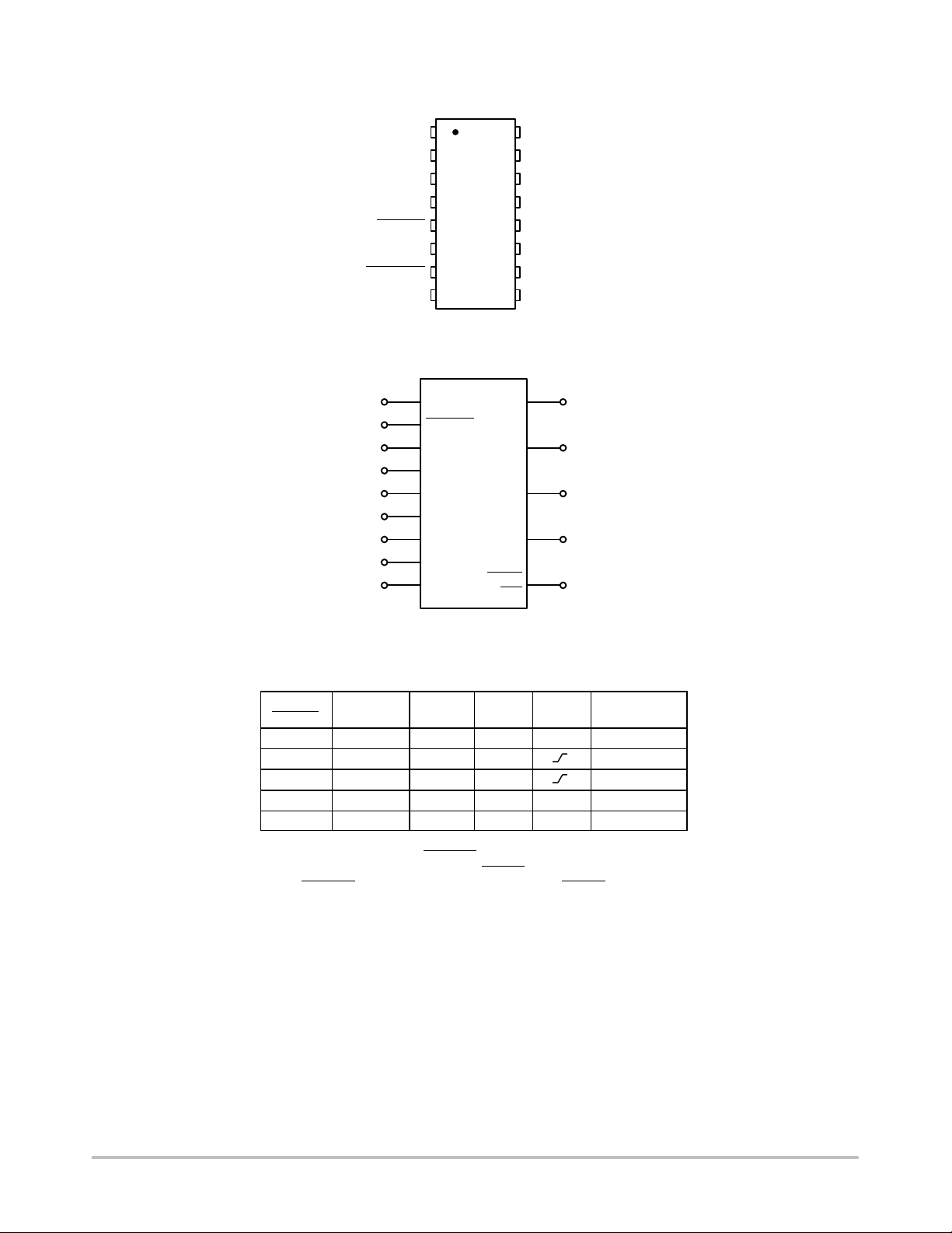
PE
Q3
CARRY IN
Q0
CARRY OUT
V
MC14516B
PIN ASSIGNMENT
1
2
P3
3
P0
4
6
7
8
SS
BLOCK DIAGRAM
16
15
14
13
125
11
10
9
V
C
Q2
P2
P1
Q1
U/D
R
DD
1
5
9
10
15
4
12
13
3
PE
CARRY IN
RESET
UP/DOWN
CLOCK
P0
P1
P2
P3
VDD = PIN 16
VSS = PIN 8
Q0
Q1
Q2
Q3
CARRY
OUT
6
11
14
2
7
TRUTH TABLE
Preset
Carry In Up/Down
1 X 0 0 X No Count
0 1 0 0 Count Up
0 0 0 0 Count Down
X X 1 0 X Preset
X X X 1 X Reset
X = Don’t Care
NOTE: When counting up, the Carry Out
when Q0 through Q3 are high and Carry In
Carry Out
is low only when Q0 through Q3 and Carry In are low.
Enable
Reset Clock Action
signal is normally high and is low only
is lo w. When counting down,
http://onsemi.com
2
MC14516B
V
ELECTRICAL CHARACTERISTICS (Voltages Referenced to V
DD
Characteristic Symbol
Output Voltage “0” Level
V
= VDD or 0
in
“1” Level
V
= 0 or V
in
DD
Input Voltage “0” Level
= 4.5 or 0.5 Vdc)
(V
O
(V
= 9.0 or 1.0 Vdc)
O
(V
= 13.5 or 1.5 Vdc)
O
“1” Level
= 0.5 or 4.5 Vdc)
(V
O
(V
= 1.0 or 9.0 Vdc)
O
(V
= 1.5 or 13.5 Vdc)
O
Output Drive Current
(V
= 2.5 Vdc) Source
OH
= 4.6 Vdc)
(V
OH
(V
= 9.5 Vdc)
OH
(V
= 13.5 Vdc)
OH
(VOL = 0.4 Vdc) Sink
(V
= 0.5 Vdc)
OL
(V
= 1.5 Vdc)
OL
Input Current I
Input Capacitance
(V
= 0)
in
Quiescent Current
(Per Package)
Total Supply Current
(5.) (6.)
(Dynamic plus Quiescent,
Per Package)
(C
= 50 pF on all outputs, all
L
Vdc
V
OL
5.0
10
15
V
OH
5.0
10
15
V
IL
5.0
10
15
V
IH
5.0
10
15
I
OH
5.0
5.0
10
15
I
OL
5.0
10
15
in
C
in
I
DD
15 — ± 0.1 — ±0.00001 ± 0.1 — ± 1.0 µAdc
— — — — 5.0 7.5 — — pF
5.0
10
15
I
T
5.0
10
15
Min Max Min Typ
—
—
—
4.95
9.95
14.95
—
—
—
3.5
7.0
11
– 3.0
– 0.64
– 1.6
– 4.2
0.64
1.6
4.2
—
—
—
)
SS
– 55C 25C 125C
(4.)
Max Min Max
0.05
0.05
0.05
—
—
—
1.5
3.0
4.0
—
—
—
—
—
—
—
—
—
—
5.0
10
20
—
—
—
4.95
9.95
14.95
—
—
—
3.5
7.0
11
– 2.4
– 0.51
– 1.3
– 3.4
0.51
1.3
3.4
—
—
—
0
0
0
5.0
10
15
2.25
4.50
6.75
2.75
5.50
8.25
– 4.2
– 0.88
– 2.25
– 8.8
0.88
2.25
8.8
0.005
0.010
0.015
IT = (0.58 µA/kHz) f + I
IT = (1.20 µA/kHz) f + I
IT = (1.70 µA/kHz) f + I
0.05
0.05
0.05
—
—
—
1.5
3.0
4.0
—
—
—
—
—
—
—
—
—
—
5.0
10
20
DD
DD
DD
—
—
—
4.95
9.95
14.95
—
—
—
3.5
7.0
11
– 1.7
– 0.36
– 0.9
– 2.4
0.36
0.9
2.4
—
—
—
0.05
0.05
0.05
buffers switching)
4. Data labelled “Typ” is not to be used for design purposes but is intended as an indication of the IC’s potential performance.
5. The formulas given are for the typical characteristics only at 25C.
6. To calculate total supply current at loads other than 50 pF:
IT(CL) = IT(50 pF) + (CL – 50) Vfk
where: I
is in µA (per package), CL in pF, V = (VDD – VSS) in volts, f in kHz is input frequency, and k = 0.001.
T
—
—
—
1.5
3.0
4.0
—
—
—
—
—
—
—
—
—
—
150
300
600
Unit
Vdc
Vdc
Vdc
Vdc
mAdc
mAdc
µAdc
µAdc
http://onsemi.com
3
MC14516B
PLH PHL
()
L
PLH,PHL
()
L
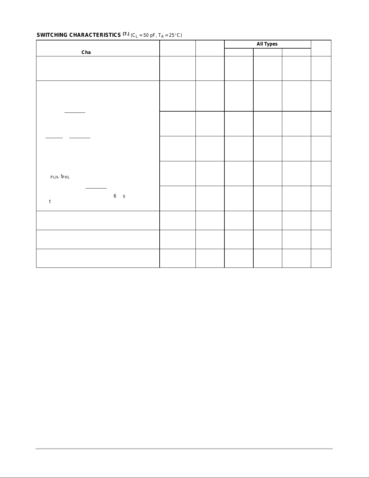
SWITCHING CHARACTERISTICS
(7.)
(C
= 50 pF, T
L
= 25C)
A
All Types
100
50
40
315
130
100
315
130
100
180
80
60
315
130
100
550
225
150
190
100
80
200
100
75
3.0
6.0
8.0
(8.)
Max
200
100
80
630
260
200
630
260
200
360
160
120
630
360
200
1100
450
300
—
—
—
—
—
—
1.5
3.0
4.0
Characteristic Symbol V
Output Rise and Fall Time
t
, t
TLH
t
TLH
t
TLH
= (1.5 ns/pF) CL + 25 ns
THL
, t
= (0.75 ns/pF) CL + 12.5 ns
THL
, t
= (0.55 ns/pF) CL + 9.5 ns
THL
Propagation Delay Time
Clock to Q
, t
t
PLH
t
PLH
t
PLH
= (1.7 ns/pF) CL + 230 ns
PHL
, t
= (0.66 ns/pF) CL + 97 ns
PHL
, t
= (0.5 ns/pF) CL + 75 ns
PHL
Clock to Carry Out
t
, t
PLH
t
PLH
t
PLH
= (1.7 ns/pF) CL + 230 ns
PHL
, t
= (0.66 ns/pF) CL + 97 ns
PHL
, t
= (0.5 ns/pF) CL + 75 ns
PHL
Carry In to Carry Out
t
, t
PLH
t
PLH
t
PLH
= (1.7 ns/pF) CL + 230 ns
PHL
, t
= (0.66 ns/pF) CL + 97 ns
PHL
, t
= (0.5 ns/pF) CL + 75 ns
PHL
Preset or Reset to Q
, t
t
PLH
t
PLH
t
PLH
= (1.7 ns/pF) CL + 230 ns
PHL
, t
= (0.66 ns/pF) CL + 97 ns
PHL
, t
= (0.5 ns/pF) CL + 75 ns
PHL
Preset or Reset to Carry Out
t
, t
PLH
t
PLH
t
PLH
= (1.7 ns/pF) CL + 465 ns
PHL
, t
= (0.66 ns/pF) CL + 192 ns
PHL
, t
= (0.5 ns/pF) CL + 125 ns
PHL
Reset Pulse Width t
Clock Pulse Width t
Clock Pulse Frequency f
t
t
t
PLH
t
t
PLH
t
t
PLH
t
t
PLH
t
t
PLH
t
TLH
THL
PHL
PHL
PHL
PHL
PHL
WH
DD
Min Typ
,
5.0
10
15
—
—
—
,
5.0
10
15
—
—
—
,
5.0
10
15
—
—
—
,
5.0
10
15
—
—
—
,
5.0
10
15
—
—
—
,
5.0
10
15
w
5.0
10
15
5.0
10
15
cl
5.0
10
15
—
—
—
380
200
160
350
170
140
—
—
—
7. The formulas given are for the typical characteristics only at 25C.
8. Data labelled “Typ” is not to be used for design purposes but is intended as an Indication of the IC’s potential performance.
Unit
ns
ns
ns
ns
ns
ns
ns
ns
MHz
http://onsemi.com
4

MC14516B
SWITCHING CHARACTERISTICS
(9.)
(C
= 50 pF, T
L
= 25C) (continued)
A
All Types
Characteristic Symbol V
Preset or Reset Removal Time
The Preset or Reset signal must be low prior to a
positive–going transition of the clock.
Clock Rise and Fall Time t
Setup Time
to Clock
Carry In
Hold Time
Clock to Carry In
Setup Time
Up/Down to Clock
Hold Time
Clock to Up/Down
Setup Time
Pn to PE
Hold Time
PE to Pn
Preset Enable Pulse Width t
t
rem
TLH
t
THL
t
t
t
WH
DD
5.0
10
15
,
5.0
10
15
su
5.0
10
15
t
h
5.0
10
15
su
5.0
10
15
t
h
5.0
10
15
su
5.0
10
15
t
h
5.0
10
15
5.0
10
15
Min Typ
650
230
180
—
—
—
260
120
100
0
20
20
500
200
150
– 70
– 10
0
– 40
– 30
– 25
480
420
420
200
100
80
(10.)
325
115
90
—
—
—
130
60
50
– 60
– 20
0
250
100
75
– 160
– 60
– 40
– 120
– 70
– 50
240
210
210
100
50
40
Max
—
—
15
5
4
—
—
—
—
—
—
—
—
—
—
—
—
—
—
—
—
—
—
—
—
—
9. The formulas given are for the typical characteristics only at 25C.
10.Data labelled “Typ” is not to be used for design purposes but is intended as an Indication of the IC’s potential performance.
Unit
ns
µs
ns
ns
ns
ns
ns
ns
ns
http://onsemi.com
5
MC14516B
V
DD
PULSE
GENERATOR
RESET
500 pF
I
D
0.01 µF
CERAMIC
PE
CARRY IN
R
UP/DOWN
CLOCK
P0
P1
P2
P3
Q0
Q1
Q2
Q3
CARRY
OUT
10%
20 ns
V
DD
V
SS
20 ns
C
L
C
L
C
L
C
L
C
L
CLOCK
50%
90%
VARIABLE
WIDTH
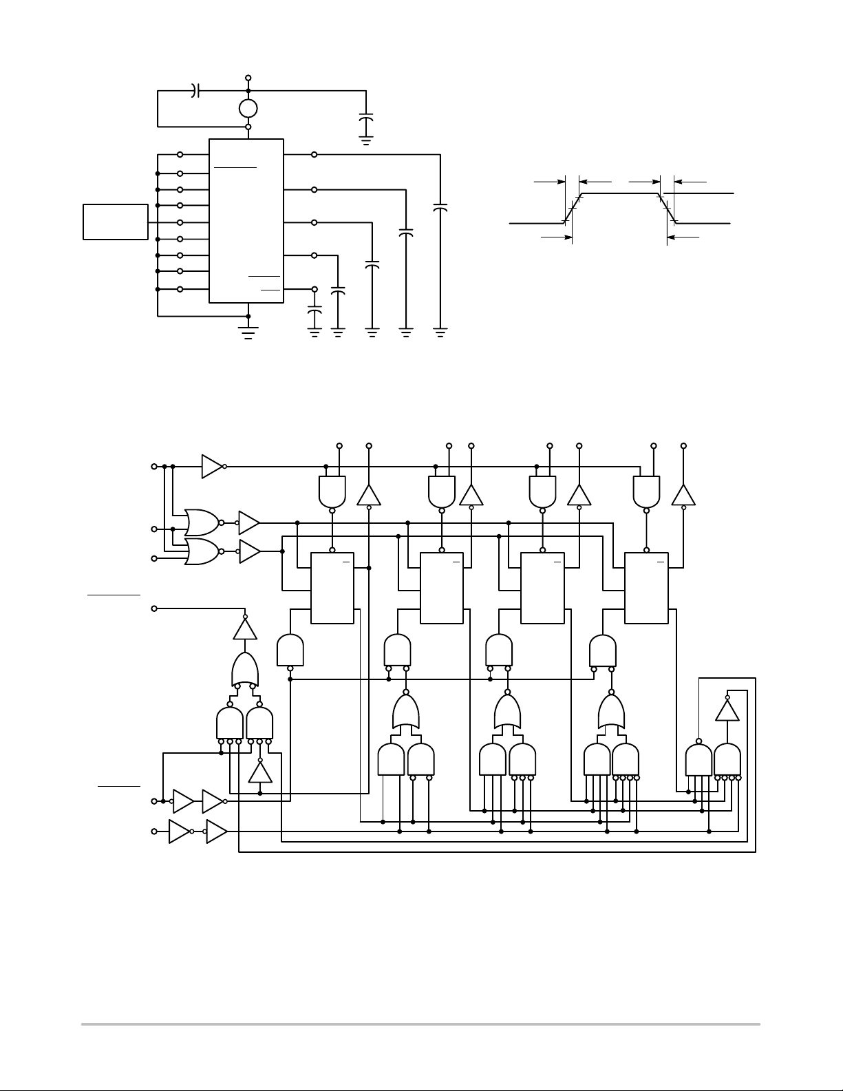
Figure 1. Power Dissipation Test Circuit and Waveform
LOGIC DIAGRAM
Q2
P04Q0
6
P1
12
Q1
11
9
P2
13
14
2
P33Q3
PRESET
ENABLE
CLOCK
CARRY OUT
CARRY IN
UP/DOWN
1
15
P
PE
Q
7
C
T
Q
P
PE
C
TQQ
P
PE
C
TQQ
P
PE
C
TQQ
5
10
http://onsemi.com
6

MC14516B
TOGGLE FLIP–FLOP
PARALLEL IN
CARRY IN
UP/DOWN
CLOCK
PRESET ENABLE
Q
OR CARRY OUT
0
RESET
OR
50%
FLIP–FLOP FUNCTIONAL TRUTH TABLE
Preset
P
PE
Q
C
Q
T
t
su
50%
50%
t
w(H)
CARRY OUT
90%
10%
t
THL
t
w
t
h
t
w(H)
ONLY
t
PLH
t
rem
t
rem
Enable
1 X X Parallel In
0 0 Q
0 1 Q
0 X Q
X = Don’t Care
1
f
Clock T Q
cl
t
TLH
90%
10%
t
PHL
t
PLH
n+1
n
n
n
V
DD
V
SS
V
DD
V
SS
V
DD
V
SS
V
OH
V
OL
V
DD
V
SS
Figure 2. Switching Time Waveforms
PIN DESCRIPTIONS
INPUTS
P0, P1, P2, P3, Preset Inputs (Pins 4, 12, 13, 3) — Data
on these inputs is loaded into the counter when PE is taken
high.
Carry In
, (Pin 5) — This active–low input is used when
Cascading stages. Carry In is usually connected to Carry Out
of the previous stage. While high, Clock is inhibited.
Clock, (Pin 15) — Binary data is incremented or
decremented, depending on the direction of count, on the
positive transition of this input.
OUTPUTS
Q0, Q1, Q2, Q3, Binary outputs (Pins 6, 11, 14, 2) —
Binary data is present on these outputs with Q0
corresponding to the least significant bit.
Carry Out, (Pin 7) — Used when cascading stages, Carry
Out is usually connected to Carry In of the next stage. This
synchronous output is active low and may also be used to
indicate terminal count.
CONTROLS
PE, Preset Enable, (Pin 1) — Asynchronously loads data
on the Preset Inputs. This pin is active high and inhibits the
clock when high.
R, Reset, (Pin 9) — Asynchronously resets the Q out–
puts to a low state. This pin is active high and inhibits the
clock when high.
Up/Down, (Pin 10) — Controls the direction of count,
high for up count, low for down count.
SUPPLY PINS
VSS, Negative Supply Voltage, (Pin 8) — This pin is
usually connected to ground.
V
, Positive Supply Voltage, (Pin 16) — This pin is
DD
connected to a positive supply voltage ranging from 3.0
volts to 18.0 volts.
http://onsemi.com
7

PRESET
ENABLE
0 = COUNT
1 = PRESET
1 = UP
0 = DOWN
MC14516B
Q0 Q1 Q2 Q3 Q4 Q5 Q6 Q7
Q0 Q1 Q2 Q3
PE
C
C
in
CLOCK
L.S.D.
MC14516B
out
U/D
R
P0 P1 P2 P3
P0 P1 P2 P3 P4 P5 P6 P7
Q0 Q1 Q2 Q3
PE
C
in
CLOCK
M.S.D.
MC14516B
U/D
R
P0 P1 P2 P3
out
TERMINAL COUNT
INDICATOR
C
+V
DD
+V
DD
THUMBWHEEL SWITCHES
(OPEN FOR 0")
RESISTORS = 10 k
+V
CLOCK
RESET
DD
OPEN = COUNT
NOTE: The Least Significant Digit (L.S.D.) counts from a preset value once Preset Enable (PE) goes low. The Most Significant
Digit (M.S.D.) is disabled while C
up mode), C
goes low for one complete clock cycle, thus allowing the next counter to decrement/increment one count.
out
is high. When the count of the L.S.D. reaches 0 (count down mode) or reaches 15 (count
in
(See Timing Diagram) The L.S.D. now counts through another cycle (15 clock pulses) and the above cycle is repeated.
Figure 3. Presettable Cascaded 8–Bit Up/Down Counter
http://onsemi.com
8

CLOCK
UP/DOWN
CARRY IN
http://onsemi.com
CARRY OUT
9
CARRY OUT
RESET
(MSD)
PE
P7
P6
P5
P4
P3
P2
P1
P0
(MSD)
Q7
Q6
Q5
Q4
Q3
Q2
Q1
Q0
(LSD)
TIMING DIAGRAM FOR THE PRESETTABLE CASCADED 8–BIT UP/DOWN COUNTER
MC14516B
COUNT
13 14 15 16 17 18 18 17 16 15 14 1319 251 252 253 254 255 0 1 2 2 13 012
PRESET ENABLE
UP COUNT DOWN COUNT UP COUNT
PRESET
ENABLE
DOWN
COUNT
UP COUNT
RESET

MC14516B
f
out
CLOCK (f
+V
DD
)
in
RESET
OPEN = COUNT
Q0 Q1 Q2 Q3 Q4 Q5 Q6 Q7
Q0 Q1 Q2 Q3
PE
C
in
CLOCK
L.S.D.
MC14516B
U/D
R
P0 P1 P2 P3
P0 P1 P2 P3
+V
DD
THUMBWHEEL SWITCHES
(OPEN FOR 0")
C
out
Q0 Q1 Q2 Q3
PE
C
in
CLOCK
M.S.D.
MC14516B
U/D
R
P0 P1 P2 P3
P4 P5 P6 P7
+V
DD
RESISTORS = 10 k
f
in
=
f
out
n
BUFFER
C
out
NOTE: The programmable frequency divider can be set by applying the desired divide ratio, in binary, to the preset inputs. For example,
the maximum divide ratio of 255 may be obtained by applying a 1111 1111 to the preset inputs P0 to P7. For this divide operation,
both counters should be configured in the count down mode. The divide ratio of zero is an undefined state and should be avoided.
Figure 4. Programmable Cascaded Frequency Divider
http://onsemi.com
10
–T–
–A–
916
B
18
F
C
S
–T–
H
G
D
16 PL
0.25 (0.010) T
K
M
–A–
16 9
–B–
18
G
K
C
SEATING
PLANE
D
16 PL
0.25 (0.010) A
M
S
B
T
S
MC14516B
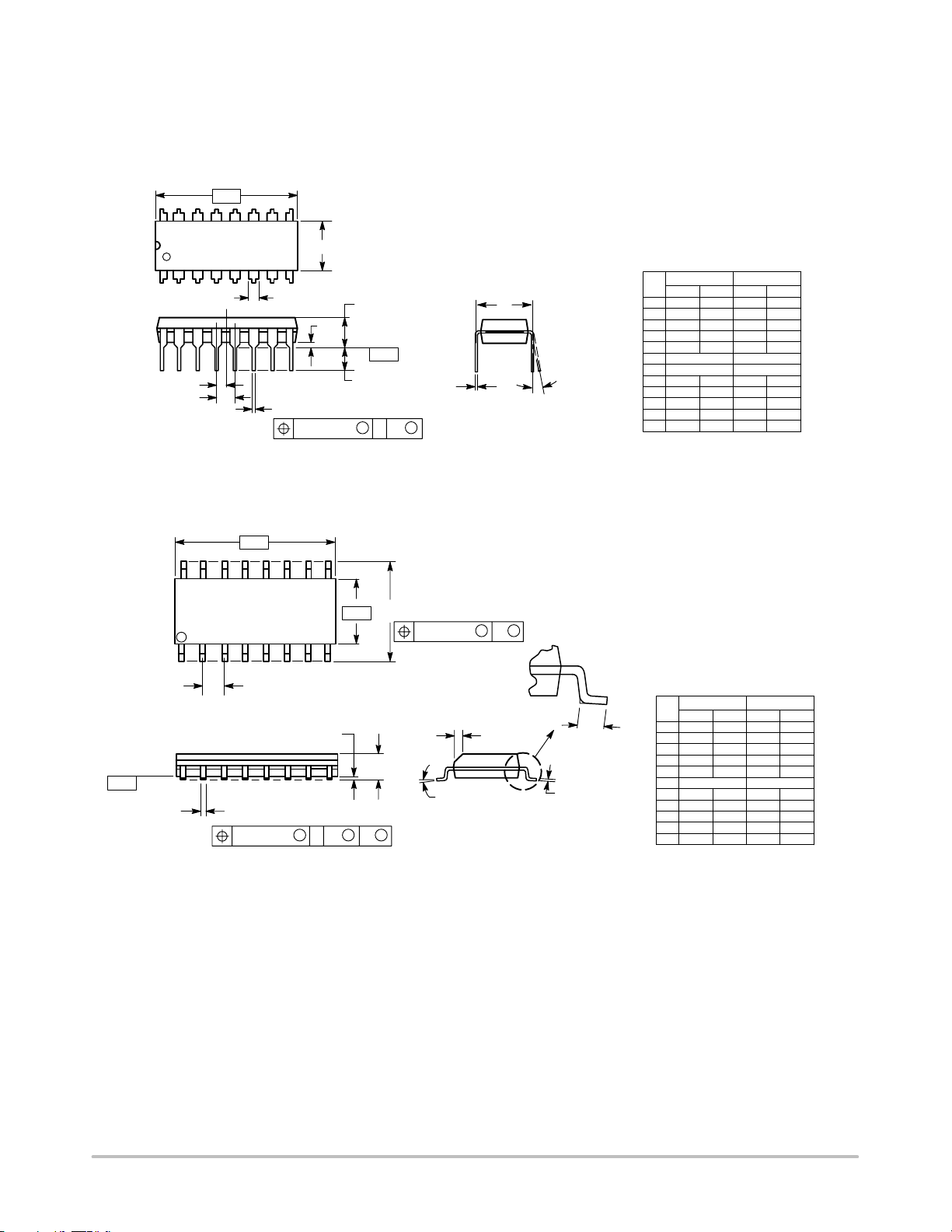
PACKAGE DIMENSIONS
PDIP–16
P SUFFIX
PLASTIC DIP PACKAGE
CASE 648–08
ISSUE R
L
SEATING
PLANE
J
M
A
SOIC–16
D SUFFIX
PLASTIC SOIC PACKAGE
CASE 751B–05
ISSUE J
8 PLP
M
0.25 (0.010) B
M
S
X 45
R
NOTES:
1. DIMENSIONING AND TOLERANCING PER ANSI
Y14.5M, 1982.
2. CONTROLLING DIMENSION: INCH.
3. DIMENSION L TO CENTER OF LEADS WHEN
FORMED PARALLEL.
4. DIMENSION B DOES NOT INCLUDE MOLD FLASH.
5. ROUNDED CORNERS OPTIONAL.
DIM MIN MAX MIN MAX
A 0.740 0.770 18.80 19.55
B 0.250 0.270 6.35 6.85
C 0.145 0.175 3.69 4.44
D 0.015 0.021 0.39 0.53
F 0.040 0.70 1.02 1.77
G 0.100 BSC 2.54 BSC
M
F
J
H 0.050 BSC 1.27 BSC
J 0.008 0.015 0.21 0.38
K 0.110 0.130 2.80 3.30
L 0.295 0.305 7.50 7.74
M 0 10 0 10
S 0.020 0.040 0.51 1.01
NOTES:
1. DIMENSIONING AND TOLERANCING PER ANSI
Y14.5M, 1982.
2. CONTROLLING DIMENSION: MILLIMETER.
3. DIMENSIONS A AND B DO NOT INCLUDE
MOLD PROTRUSION.
4. MAXIMUM MOLD PROTRUSION 0.15 (0.006)
PER SIDE.
5. DIMENSION D DOES NOT INCLUDE DAMBAR
PROTRUSION. ALLOWABLE DAMBAR
PROTRUSION SHALL BE 0.127 (0.005) TOTAL
IN EXCESS OF THE D DIMENSION AT
MAXIMUM MATERIAL CONDITION.
DIM MIN MAX MIN MAX
A 9.80 10.00 0.386 0.393
B 3.80 4.00 0.150 0.157
C 1.35 1.75 0.054 0.068
D 0.35 0.49 0.014 0.019
F 0.40 1.25 0.016 0.049
G 1.27 BSC 0.050 BSC
J 0.19 0.25 0.008 0.009
K 0.10 0.25 0.004 0.009
M 0 7 0 7
P 5.80 6.20 0.229 0.244
R 0.25 0.50 0.010 0.019
MILLIMETERSINCHES
INCHESMILLIMETERS
http://onsemi.com
11
16 9
1
Z
D
e
b
0.13 (0.005)
M
8
H
E
E
A
A
1
0.10 (0.004)
MC14516B
PACKAGE DIMENSIONS
SOEIAJ–16
F SUFFIX
PLASTIC EIAJ SOIC PACKAGE
CASE 966–01
ISSUE O
L
E
M
L
DETAIL P
VIEW P
NOTES:
1. DIMENSIONING AND TOLERANCING PER ANSI
Y14.5M, 1982.
2. CONTROLLING DIMENSION: MILLIMETER.
3. DIMENSIONS D AND E DO NOT INCLUDE
MOLD FLASH OR PROTRUSIONS AND ARE
Q
1
c
MEASURED AT THE PARTING LINE. MOLD FLASH
OR PROTRUSIONS SHALL NOT EXCEED 0.15
(0.006) PER SIDE.
4. TERMINAL NUMBERS ARE SHOWN FOR
REFERENCE ONLY.
5. THE LEAD WIDTH DIMENSION (b) DOES NOT
INCLUDE DAMBAR PROTRUSION. ALLOWABLE
DAMBAR PROTRUSION SHALL BE 0.08 (0.003)
TOTAL IN EXCESS OF THE LEAD WIDTH
DIMENSION AT MAXIMUM MATERIAL CONDITION.
DAMBAR CANNOT BE LOCATED ON THE LOWER
RADIUS OR THE FOOT. MINIMUM SPACE
BETWEEN PROTRUSIONS AND ADJACENT LEAD
TO BE 0.46 ( 0.018).
MILLIMETERS
DIM MIN MAX MIN MAX
--- 2.05 --- 0.081
A
A
0.05 0.20 0.002 0.008
1
0.35 0.50 0.014 0.020
b
0.18 0.27 0.007 0.011
c
9.90 10.50 0.390 0.413
D
5.10 5.45 0.201 0.215
E
1.27 BSC 0.050 BSC
e
H
7.40 8.20 0.291 0.323
E
0.50 0.85 0.020 0.033
L
L
1.10 1.50 0.043 0.059
E
0
M
Q
0.70 0.90 0.028 0.035
1
--- 0.78 --- 0.031
Z
INCHES
10
10
0
ON Semiconductor and are trademarks of Semiconductor Components Industries, LLC (SCILLC). SCILLC reserves the right to make changes
without further notice to any products herein. SCILLC makes no warranty, representation or guarantee regarding the suitability of its products for any particular
purpose, nor does SCILLC assume any liability arising out of the application or use of any product or circuit, and specifically disclaims any and all liability,
including without limitation special, consequential or incidental damages. “Typical” parameters which may be provided in SCILLC data sheets and/or
specifications can and do vary in different applications and actual performance may vary over time. All operating parameters, including “Typicals” must be
validated for each customer application by customer’s technical experts. SCILLC does not convey any license under its patent rights nor the rights of others.
SCILLC products are not designed, intended, or authorized for use as components in systems intended for surgical implant into the body, or other applications
intended to support or sustain life, or for any other application in which the failure of the SCILLC product could create a situation where personal injury or
death may occur. Should Buyer purchase or use SCILLC products for any such unintended or unauthorized application, Buyer shall indemnify and hold
SCILLC and its officers, employees, subsidiaries, affiliates, and distributors harmless against all claims, costs, damages, and expenses, and reasonable
attorney fees arising out of, directly or indirectly, any claim of personal injury or death associated with such unintended or unauthorized use, even if such claim
alleges that SCILLC was negligent regarding the design or manufacture of the part. SCILLC is an Equal Opportunity/Affirmative Action Employer.
PUBLICATION ORDERING INFORMATION
NORTH AMERICA Literature Fulfillment:
Literature Distribution Center for ON Semiconductor
P.O. Box 5163, Denver, Colorado 80217 USA
Phone: 303–675–2175 or 800–344–3860 Toll Free USA/Canada
Fax: 303–675–2176 or 800–344–3867 Toll Free USA/Canada
Email: ONlit@hibbertco.com
Fax Response Line: 303–675–2167 or 800–344–3810 Toll Free USA/Canada
N. American Technical Support: 800–282–9855 Toll Free USA/Canada
EUROPE: LDC for ON Semiconductor – European Support
German Phone: (+1) 303–308–7140 (Mon–Fri 2:30pm to 7:00pm CET)
Email: ONlit–german@hibbertco.com
French Phone: (+1) 303–308–7141 (Mon–Fri 2:00pm to 7:00pm CET)
Email: ONlit–french@hibbertco.com
English Phone: (+1) 303–308–7142 (Mon–Fri 12:00pm to 5:00pm GMT)
Email: ONlit@hibbertco.com
EUROPEAN TOLL–FREE ACCESS*: 00–800–4422–3781
*Available from Germany, France, Italy, UK
CENTRAL/SOUTH AMERICA:
Spanish Phone: 303–308–7143 (Mon–Fri 8:00am to 5:00pm MST)
Email: ONlit–spanish@hibbertco.com
ASIA/PACIFIC: LDC for ON Semiconductor – Asia Support
Phone: 303–675–2121 (Tue–Fri 9:00am to 1:00pm, Hong Kong Time)
Toll Free from Hong Kong & Singapore:
001–800–4422–3781
Email: ONlit–asia@hibbertco.com
JAPAN: ON Semiconductor, Japan Customer Focus Center
4–32–1 Nishi–Gotanda, Shinagawa–ku, Tokyo, Japan 141–0031
Phone: 81–3–5740–2745
Email: r14525@onsemi.com
ON Semiconductor Website: http://onsemi.com
For additional information, please contact your local
Sales Representative.
http://onsemi.com
12
MC14516B/D
 Loading...