

MC14001B Series
B-Suffix Series CMOS Gates
MC14001B, MC14011B, MC14023B,
MC14025B, MC14071B, MC14073B,
MC14081B, MC14082B
The B Series logic gates are constructed with P and N channel
enhancement mode devices in a single monolithic structure
(Complementary MOS). Their primary use is where low power
dissipation and/or high noise immunity is desired.
Features
• Supply Voltage Range = 3.0 Vdc to 18 Vdc
• All Outputs Buffered
• Capable of Driving Two Low−power TTL Loads or One Low−power
Schottky TTL Load Over the Rated Temperature Range.
• Double Diode Protection on All Inputs Except: Triple Diode
Protection on MC14011B and MC14081B
• Pin−for−Pin Replacements for Corresponding CD4000 Series
B Suffix Devices
• These Devices are Pb−Free and are RoHS Compliant
• NLV Prefix for Automotive and Other Applications Requiring
Unique Site and Control Change Requirements; AEC−Q100
Qualified and PPAP Capable
MAXIMUM RATINGS (Voltages Referenced to V
Symbol
V
Vin, V
Iin, I
T
V
Stresses exceeding Maximum Ratings may damage the device. Maximum
Ratings are stress ratings only. Functional operation above the Recommended
Operating Conditions is not implied. Extended exposure to stresses above the
Recommended Operating Conditions may affect device reliability.
1. Temperature Derating:
Plastic “P and D/DW” Packages: – 7.0 mW/_C From 65_C To 125_C
This device contains protection circuitry to guard against damage due to high
static voltages or electric fields. However, precautions must be taken to avoid
applications of any voltage higher than maximum rated voltages to this
high−impedance circuit. For proper operation, V
to the range V
Unused inputs must always be tied to an appropriate logic voltage level
(e.g., either V
DC Supply Voltage Range −0.5 to +18.0 V
DD
Input or Output Voltage Range
out
(DC or Transient)
Input or Output Current
out
(DC or Transient) per Pin
P
Power Dissipation, per Package
D
(Note 1)
T
Ambient Temperature Range −55 to +125 °C
A
Storage Temperature Range −65 to +150 °C
stg
T
Lead Temperature
L
(8−Second Soldering)
ESD Withstand Voltage
ESD
SS
SS
Parameter Value Unit
Human Body Model
Machine Model
Charged Device Model
v (Vin or V
or VDD). Unused outputs must be left open.
) v VDD.
out
)
SS
−0.5 to VDD + 0.5 V
± 10 mA
500 mW
260 °C
> 3000
> 300
N/A
and V
in
should be constrained
out
V
http://onsemi.com
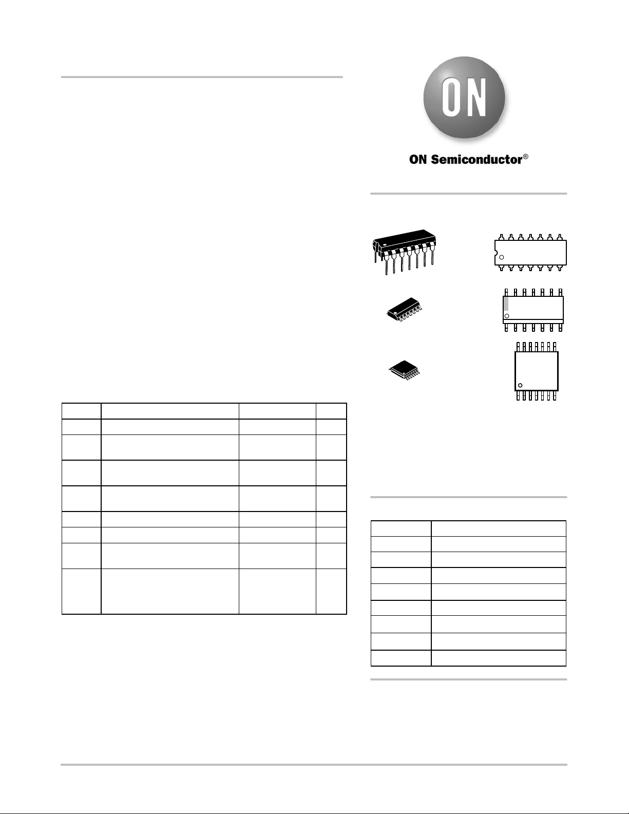
MARKING
DIAGRAMS
14
PDIP−14
P SUFFIX
CASE 646
SOIC−14
D SUFFIX
CASE 751A
TSSOP−14
DT SUFFIX
CASE 948G
xx = Specific Device Code
A = Assembly Location
WL, L = Wafer Lot
YY, Y = Year
WW, W = Work Week
G or G = Pb−Free Package
(Note: Microdot may be in either location)
MC140xxBCP
AWLYYWWG
1
14
140xxBG
AWLYWW
1
14
14
0xxB
ALYWG
G
1
DEVICE INFORMATION
Device Description
MC14001B Quad 2−Input NOR Gate
MC14011B Quad 2−Input NAND Gate
MC14023B Triple 3−Input NAND Gate
MC14025B Triple 3−Input NOR Gate
MC14071B Quad 2−Input OR Gate
MC14073B Triple 3−Input AND Gate
MC14081B Quad 2−Input AND Gate
MC14082B Dual 4−Input AND Gate
ORDERING INFORMATION
See detailed ordering and shipping information in the package
dimensions section on page 8 of this data sheet.
© Semiconductor Components Industries, LLC, 2013
April, 2013 − Rev. 10
1 Publication Order Number:
MC14001B/D
MC14001B Series
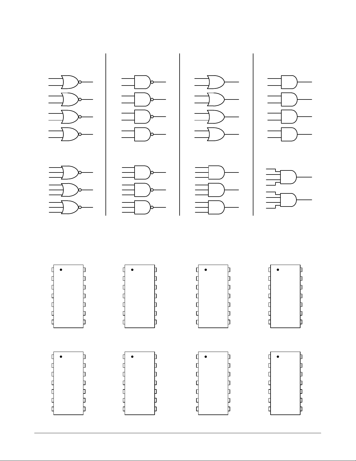
LOGIC DIAGRAMS
NOR
MC14001B
Quad 2−Input NOR Gate
1
2
5
6
2 INPUT
8
9
12
13
MC14025B
Triple 3−Input NOR Gate
1
2
8
3
4
5
3 INPUT
11
12
13
NAND
MC14011B
Quad 2−Input NAND Gate
3
4
10
11
1
2
5
6
8
9
12
13
3
4
10
11
Quad 2−Input OR Gate
1
2
5
6
8
9
12
13
MC14023B
Triple 3−Input NAND Gate
1
9
6
10
2
9
8
3
4
6
5
11
12
10
13
Triple 3−Input AND Gate
1
2
8
3
4
5
11
12
13
OR
MC14071B
MC14073B
AND
MC14081B
Quad 2−Input AND Gate
3
4
10
11
1
2
5
6
8
9
12
13
3
4
10
11
MC14082B
Dual 4−Input AND Gate
9
6
10
2
3
4
1
5
9
10
11
12
NC = 6, 8
13
VDD = PIN 14
V
= PIN 7
SS
FOR ALL DEVICES
MC14001B
Quad 2−Input NOR Gate
IN 1
IN 2
OUT
OUT
IN 1
IN 2
V
1
A
2
A
3
A
4
B
B
6
B
7
SS
14
V
DD
IN 2
13
IN 1
12
11
OUT
OUT
105
9
IN 2
8
IN 1
MC14071B
Quad 2−Input OR Gate
IN 1
IN 2
OUT
OUT
IN 1
IN 2
V
1
A
2
A
3
A
4
B
B
6
B
7
SS
14
V
DD
13
IN 2
12
IN 1
11
OUT
OUT
105
9
IN 2
8
IN 1
MC14011B
Quad 2−Input NAND Gate
1
IN 1
A
2
D
D
C
C
IN 2
A
3
OUT
A
4
OUT
D
C
IN 1
IN 2
B
B
6
B
7
V
SS
MC14073B
Triple 3−Input AND Gate
1
IN 1
A
2
D
D
C
C
IN 2
A
3
IN 1
B
4
IN 2
D
C
IN 3
OUT
B
B
6
B
7
V
SS
PIN ASSIGNMENTS
Triple 3−Input NAND Gate
14
V
DD
13
IN 2
D
12
IN 1
D
11
OUT
D
OUT
105
14
13
12
11
105
C
9
IN 2
C
8
IN 1
C
V
DD
IN 3
C
IN 2
C
IN 1
C
OUT
C
9
OUT
A
8
IN 3
A
IN 1
A
IN 2
A
IN 1
B
IN 2
B
IN 3
B
OUT
B
V
SS
Quad 2−Input AND Gate
IN 1
A
IN 2
A
OUT
A
OUT
B
IN 1
B
IN 2
B
V
SS
MC14023B
1
2
3
4
6
7
MC14081B
1
2
3
4
6
7
MC14025B
Triple 3−Input NOR Gate
1
14
V
DD
13
IN 3
C
12
IN 2
C
11
IN 1
C
OUT
105
C
9
OUT
A
8
IN 3
A
IN 1
IN 2
IN 1
IN 2
IN 3
OUT
A
2
A
3
B
4
B
B
6
B
7
V
SS
14
V
DD
IN 3
13
C
IN 2
12
C
11
IN 1
C
OUT
105
C
9
OUT
A
8
IN 3
A
MC14082B
Dual 4−Input AND Gate
1
14
V
DD
13
IN 2
D
12
IN 1
D
11
OUT
D
OUT
105
C
9
IN 2
C
8
IN 1
C
OUT
IN 1
IN 2
IN 3
IN 4
A
2
A
3
A
4
A
A
6
NC
7
V
SS
14
V
DD
13
OUT
B
12
IN 4
B
11
IN 3
B
IN 2
105
B
9
IN 1
B
8
NC
http://onsemi.com
2
NC = NO CONNECTION
MC14001B Series
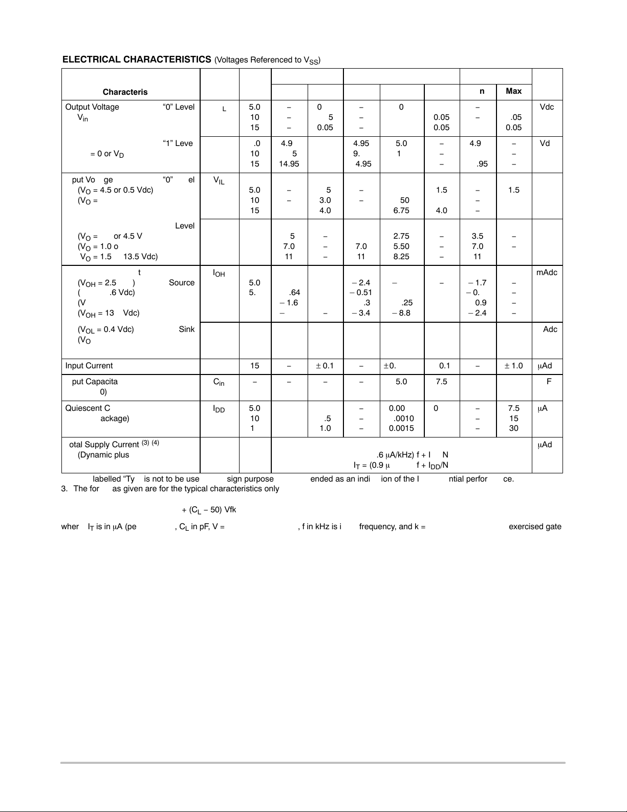
ELECTRICAL CHARACTERISTICS (Voltages Referenced to V
V
DD
Characteristic
Output Voltage “0” Level
V
= VDD or 0
in
“1” Level
V
= 0 or V
in
DD
Input Voltage “0” Level
(V
= 4.5 or 0.5 Vdc)
O
= 9.0 or 1.0 Vdc)
(V
O
(V
= 13.5 or 1.5 Vdc)
O
“1” Level
(V
= 0.5 or 4.5 Vdc)
O
= 1.0 or 9.0 Vdc)
(V
O
(V
= 1.5 or 13.5 Vdc)
O
Output Drive Current
(V
= 2.5 Vdc) Source
OH
= 4.6 Vdc)
(V
OH
(V
= 9.5 Vdc)
OH
(V
= 13.5 Vdc)
OH
(VOL = 0.4 Vdc) Sink
(V
= 0.5 Vdc)
OL
= 1.5 Vdc)
(V
OL
Input Current
Input Capacitance
(V
= 0)
in
Quiescent Current
(Per Package)
Total Supply Current
(3) (4)
(Dynamic plus Quiescent,
Per Gate, C
= 50 pF)
L
Symbol
V
OL
V
OH
V
IL
V
IH
I
OH
I
OL
I
in
C
in
I
DD
I
T
Vdc
5.0
10
15
5.0
10
15
5.0
10
15
5.0
10
15
5.0
5.0
10
15
5.0
10
15
15
5.0
10
15
5.0
10
15
Min
−
−
−
4.95
9.95
14.95
−
−
−
3.5
7.0
11
– 3.0
– 0.64
– 1.6
– 4.2
0.64
1.6
4.2
−
−
−
−
−
−
SS
− 55_C
)
Max
0.05
0.05
0.05
−
−
−
1.5
3.0
4.0
−
−
−
−
−
−
−
−
−
−
± 0.1
−
0.25
0.5
1.0
25_C
Min
−
−
−
4.95
9.95
14.95
−
−
−
3.5
7.0
11
– 2.4
– 0.51
– 1.3
– 3.4
0.51
1.3
3.4
−
−
−
−
−
(2)
Typ
0
0
0
5.0
10
15
2.25
4.50
6.75
2.75
5.50
8.25
– 4.2
– 0.88
– 2.25
– 8.8
0.88
2.25
8.8
± 0.00001
5.0
0.0005
0.0010
0.0015
± 0.1
IT = (0.3 mA/kHz) f + IDD/N
I
= (0.6 mA/kHz) f + IDD/N
T
I
= (0.9 mA/kHz) f + IDD/N
T
Max
0.05
0.05
0.05
−
−
−
1.5
3.0
4.0
−
−
−
−
−
−
−
−
−
−
7.5
0.25
0.5
1.0
Min
−
−
−
4.95
9.95
14.95
−
−
−
3.5
7.0
11
– 1.7
– 0.36
– 0.9
– 2.4
0.36
0.9
2.4
−
−
−
−
−
125_C
Max
0.05
0.05
0.05
−
−
−
1.5
3.0
4.0
−
−
−
−
−
−
−
−
−
−
± 1.0
−
7.5
15
30
Unit
Vdc
Vdc
Vdc
Vdc
mAdc
mAdc
mAdc
pF
mAdc
mAdc
2. Data labelled “Typ” is not to be used for design purposes but is intended as an indication of the IC’s potential performance.
3. The formulas given are for the typical characteristics only at 25_C.
4. To calculate total supply current at loads other than 50 pF:
) = IT(50 pF) + (CL − 50) Vfk
I
T(CL
where: IT is in mA (per package), CL in pF, V = (VDD − VSS) in volts, f in kHz is input frequency, and k = 0.001 x the number of exercised gates
per package.
http://onsemi.com
3
MC14001B Series
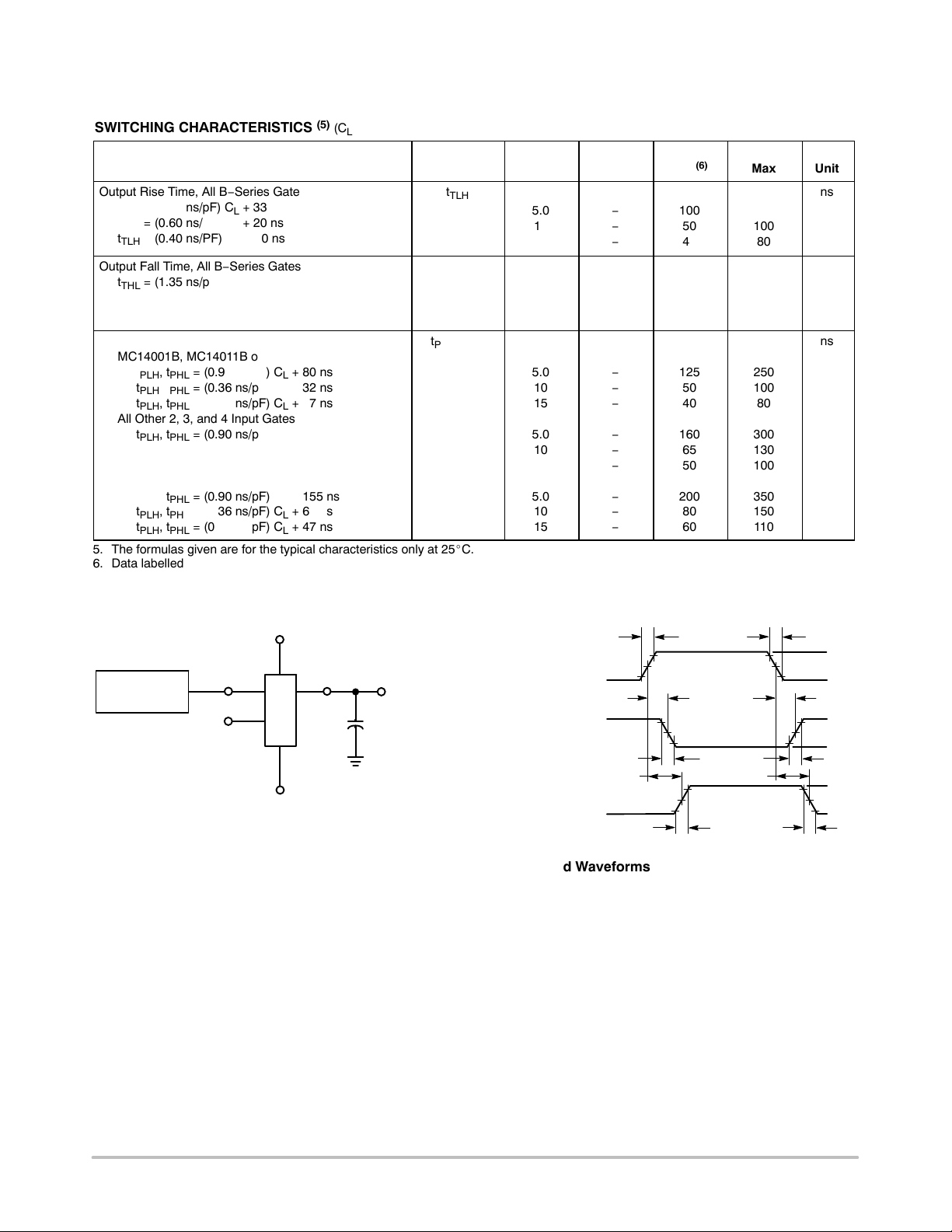
B−SERIES GATE SWITCHING TIMES
SWITCHING CHARACTERISTICS
Characteristic
Output Rise Time, All B−Series Gates
t
= (1.35 ns/pF) CL + 33 ns
TLH
= (0.60 ns/pF) CL + 20 ns
t
TLH
t
= (0.40 ns/PF) CL + 20 ns
TLH
Output Fall Time, All B−Series Gates
t
= (1.35 ns/pF) CL + 33 ns
THL
= (0.60 ns/pF) CL + 20 ns
t
THL
t
= (0.40 ns/pF) CL + 20 ns
THL
Propagation Delay Time
(5)
(CL = 50 pF, T
= 25_C)
A
t
Symbol
t
TLH
t
THL
, t
PLH
PHL
V
DD
Vdc
5.0
10
15
5.0
10
15
Min
−
−
−
−
−
−
Typ
100
50
40
100
50
40
(6)
Max
200
100
80
200
100
80
MC14001B, MC14011B only
t
, t
PLH
t
PLH
t
PLH
= (0.90 ns/pF) CL + 80 ns
PHL
, t
= (0.36 ns/pF) CL + 32 ns
PHL
, t
= (0.26 ns/pF) CL + 27 ns
PHL
5.0
10
15
−
−
−
125
50
40
250
100
80
All Other 2, 3, and 4 Input Gates
t
PLH
t
PLH
t
PLH
, t
= (0.90 ns/pF) CL + 115 ns
PHL
, t
= (0.36 ns/pF) CL + 47 ns
PHL
, t
= (0.26 ns/pF) CL + 37 ns
PHL
5.0
10
15
−
−
−
160
65
50
300
130
100
8−Input Gates (MC14068B, MC14078B)
t
PLH
t
PLH
t
PLH
, t
= (0.90 ns/pF) CL + 155 ns
PHL
, t
= (0.36 ns/pF) CL + 62 ns
PHL
, t
= (0.26 ns/pF) CL + 47 ns
PHL
5.0
10
15
−
−
−
200
80
60
350
150
110
5. The formulas given are for the typical characteristics only at 25_C.
6. Data labelled “Typ” is not to be used for design purposes but is intended as an indication of the IC’s potential performance.
Unit
ns
ns
ns
V
14
DD
PULSE
GENERATOR
INPUT
*
C
OUTPUT
L
VSS7
*All unused inputs of AND, NAND gates must be connected to VDD.
All unused inputs of OR, NOR gates must be connected to V
SS
.
Figure 1. Switching Time Test Circuit and Waveforms
20 ns 20 ns
INPUT
OUTPUT
INVERTING
OUTPUT
NON-INVERTING
t
PHL
t
t
THL
PLH
V
0 V
V
V
V
V
DD
OH
OL
OH
OL
90%
50%
10%
90%
t
TLH
50%
10%
90%
50%
10%
t
PLH
t
TLH
t
PHL
t
THL
http://onsemi.com
4

MC14001B Series
CIRCUIT SCHEMATIC
NOR, OR GATES
1, 6, 8, 13
2, 5, 9, 12
MC14001B, MC14071B
One of Four Gates Shown
V
DD
*
V
SS
*Inverter omitted in MC14001B
MC14025B
One of Three Gates Shown
V
14
V
DD
1, 3, 11
2, 4, 12
3, 4, 10, 11
V
7
SS
8, 5, 13
DD
14
V
DD
*
V
SS
V
DD
V
SS
*Inverter omitted in MC14025B
9, 6, 10
7
V
SS
2, 4, 12
1, 3, 11
8, 5, 13
MC14023B, MC14073B
One of Three Gates Shown
V
DD
V
SS
V
DD
V
SS
*Inverter omitted in MC14023B
CIRCUIT SCHEMATIC
NAND, AND GATES
14
V
DD
*
V
7
SS
2, 5, 9, 12
1, 6, 8, 13
9, 6, 10
MC14011B, MC14081B
One of Four Gates Shown
14
*
*Inverter omitted in MC14011B
7
V
DD
3, 4, 10, 11
V
SS
http://onsemi.com
5

5.0
4.0
3.0
2.0
DRAIN CURRENT (mA)
D
I ,
1.0
MC14001B Series
TYPICAL B−SERIES GATE CHARACTERISTICS
N−CHANNEL DRAIN CURRENT (SINK) P−CHANNEL DRAIN CURRENT (SOURCE)
- 10
- 9.0
- 8.0
TA = - 55°C
- 40°C
+ 25°C
+ 85°C
+ 125°C
0
1.0 3.0 5.04.02.00
VDS, DRAIN-TO-SOURCE VOLTAGE (Vdc) VDS, DRAIN-TO-SOURCE VOLTAGE (Vdc)
Figure 2. VGS = 5.0 Vdc Figure 3. VGS = − 5.0 Vdc
- 7.0
- 6.0
- 5.0
- 4.0
DRAIN CURRENT (mA)
- 3.0
D
I ,
- 2.0
- 1.0
0
0
- 1.0 - 3.0 - 5.0- 4.0- 2.0
TA = - 55°C
- 40°C
+ 85°C
+ 125°C
+ 25°C
8.0
DRAIN CURRENT (mA)
6.0
D
I ,
4.0
2.0
DRAIN CURRENT (mA)
D
I ,
5.0
20
18
16
14
12
10
0
, DRAIN-TO-SOURCE VOLTAGE (Vdc)
V
DS
5.03.01.0 108.06.04.02.00
TA = - 55°C
- 40°C
+ 25°C
+ 85°C
+ 125°C
9.07.0 - 5.0- 3.0- 1.0 - 10- 8.0- 6.0- 4.0- 2.0 - 9.0- 7.0
DRAIN CURRENT (mA)
D
I ,
- 5.0
- 50
- 45
- 40
- 35
- 30
- 25
- 20
- 15
- 10
TA = - 55°C
+ 25°C
0
0
, DRAIN-TO-SOURCE VOLTAGE (Vdc)
V
DS
- 40°C
+ 85°C
+ 125°C
Figure 4. VGS = 10 Vdc Figure 5. VGS = − 10 Vdc
50
45
40
35
30
25
20
15
10
0
0
, DRAIN-TO-SOURCE VOLTAGE (Vdc) VDS, DRAIN-TO-SOURCE VOLTAGE (Vdc)
V
DS
TA = - 55°C
- 40°C
+ 25°C
+ 85°C
+ 125°C
106.02.0 2016128.04.0 1814
- 100
DRAIN CURRENT (mA)
D
I ,
- 90
- 80
- 70
- 60
- 50
- 40
- 30
- 20
- 10
TA = - 55°C
- 40°C
+ 25°C
+ 85°C
+ 125°C
0
0
- 10- 6.0- 2.0 - 20- 16- 12- 8.0- 4.0 - 18- 14
Figure 6. VGS = 15 Vdc Figure 7. VGS = − 15 Vdc
These typical curves are not guarantees, but are design aids.
Caution: The maximum rating for output current is 10 mA per pin.
http://onsemi.com
6

MC14001B Series
TYPICAL B−SERIES GATE CHARACTERISTICS (cont’d)
VOLTAGE TRANSFER CHARACTERISTICS
5.0
4.0
3.0
OUTPUT VOLTAGE (Vdc)
2.0
out
V ,
1.0
0
16
14
12
10
8.0
6.0
OUTPUT VOLTAGE (Vdc)
4.0
out
V ,
2.0
0
0
SINGLE INPUT NAND, AND
MULTIPLE INPUT NOR, OR
SINGLE INPUT NOR, OR
MULTIPLE INPUT NAND, AND
1.0 3.0 5.04.02.00
, INPUT VOLTAGE (Vdc)
V
in
Figure 8. VDD = 5.0 Vdc Figure 9. VDD = 10 Vdc
2.0 6.0 108.04.0
, INPUT VOLTAGE (Vdc)
V
in
Figure 10. VDD = 15 Vdc
SINGLE INPUT NAND, AND
MULTIPLE INPUT NOR, OR
SINGLE INPUT NOR, OR
MULTIPLE INPUT NAND, AND
SINGLE INPUT NAND, AND
10
8.0
6.0
OUTPUT VOLTAGE (Vdc)
4.0
out
V ,
2.0
0
0
2.0 6.0 108.04.0
MULTIPLE INPUT NOR, OR
SINGLE INPUT NOR, OR
MULTIPLE INPUT NAND, AND
, INPUT VOLTAGE (Vdc)
V
in
DC NOISE MARGIN
The DC noise margin is defined as the input voltage range
from an ideal “1” or “0” input level which does not produce
output state change(s). The typical and guaranteed limit
values of the input values V
be at a fixed voltage V
Characteristics table. V
and VIH for the output(s) to
IL
are given in the Electrical
O
and VIH are presented graphically
IL
in Figure 11.
Guaranteed minimum noise margins for both the “1” and
“0” levels =
1.0 V with a 5.0 V supply
2.0 V with a 10.0 V supply
2.5 V with a 15.0 V supply
V
V
out
DD
V
O
V
O
V
DD
0
V
IL
V
V
in
IH
VSS = 0 VOLTS DC
V
V
out
DD
V
O
V
O
0
V
IL
(a) Inverting Function (b) Non−Inverting Function
Figure 11. DC Noise Immunity
http://onsemi.com
7
V
DD
V
in
V
IH

MC14001B Series
ORDERING INFORMATION
Device Package Shipping
MC14001BCPG PDIP−14
MC14001BDG
NLV14001BDG*
MC14001BDR2G
NLV14001BDR2G*
MC14001BDTR2G
NLV14001BDTR2G*
MC14001BFELG SOEIAJ−14
(Pb−Free)
SOIC−14
(Pb−Free)
SOIC−14
(Pb−Free)
TSSOP−14
(Pb−Free)
(Pb−Free)
†
25 Units / Rail
55 Units / Rail
2500 Units / Tape & Reel
2000 Units / Tape & Reel
MC14011BCPG PDIP−14
MC14011BDG
NLV14011BDG*
MC14011BDR2G
NLV14011BDR2G*
MC14011BDTR2G
NLV14011BDTR2G*
MC14011BFG
MC14011BFELG 2000 Units / Tape & Reel
MC14023BCPG PDIP−14
MC14023BDG SOIC−14
MC14023BDR2G
NLV14023BDR2G*
MC14023BFELG SOEIAJ−14
MC14025BCPG PDIP−14
MC14025BDG
NLV14025BDG*
MC14025BDR2G
NLV14025BDR2G*
MC14025BFELG SOEIAJ−14
(Pb−Free)
SOIC−14
(Pb−Free)
SOIC−14
(Pb−Free)
TSSOP−14
(Pb−Free)
SOEIAJ−14
(Pb−Free)
(Pb−Free)
(Pb−Free)
SOIC−14
(Pb−Free)
(Pb−Free)
(Pb−Free)
SOIC−14
(Pb−Free)
SOIC−14
(Pb−Free)
(Pb−Free)
25 Units / Rail
55 Units / Rail
2500 Units / Tape & Reel
50 Units / Rail
25 Units / Rail
55 Units / Rail
2500 Units / Tape & Reel
2000 Units / Tape & Reel
25 Units / Rail
55 Units / Rail
2500 Units / Tape & Reel
2000 Units / Tape & Reel
http://onsemi.com
8

MC14001B Series
ORDERING INFORMATION
Device Shipping
MC14071BCPG PDIP−14
MC14071BDG
NLV14071BDG*
MC14071BDR2G
NLV14071BDR2G*
MC14071BDTG
MC14071BDTR2G
NLV14071BDTR2G*
Package
(Pb−Free)
SOIC−14
(Pb−Free)
SOIC−14
(Pb−Free)
TSSOP−14
(Pb−Free)
†
25 Units / Rail
55 Units / Rail
2500 Units / Tape & Reel
96 Units per Rail
2500 Units / Tape & Reel
MC14073BCPG PDIP−14
MC14073BDG SOIC−14
MC14073BDR2G SOIC−14
MC14081BCPG PDIP−14
MC14081BDG
NLV14081BDG*
MC14081BDR2G
NLV14081BDR2G*
MC14081BDTR2G
NLV14081BDTR2G*
MC14082BCPG PDIP−14
MC14082BDG
NLV14082BDG*
MC14082BDR2G
†For information on tape and reel specifications, including part orientation and tape sizes, please refer to our Tape and Reel Packaging
Specifications Brochure, BRD8011/D.
*NLV Prefix for Automotive and Other Applications Requiring Unique Site and Control Change Requirements; AEC−Q100 Qualified and PPAP
Capable.
(Pb−Free)
(Pb−Free)
(Pb−Free)
(Pb−Free)
SOIC−14
(Pb−Free)
SOIC−14
(Pb−Free)
TSSOP−14
(Pb−Free)
(Pb−Free)
SOIC−14
(Pb−Free)
25 Units / Rail
55 Units / Rail
2500 Units / Tape & Reel
25 Units / Rail
55 Units / Rail
2500 Units / Tape & Reel
500 Units / Tube
55 Units / Rail
2500 Units / Tape & Reel
http://onsemi.com
9

MC14001B Series
PACKAGE DIMENSIONS
SOIC−14 NB
CASE 751A−03
ISSUE K
14
H
M
0.25 B
DETAIL A
NOTES:
1. DIMENSIONING AND TOLERANCING PER
ASME Y14.5M, 1994.
2. CONTROLLING DIMENSION: MILLIMETERS.
3. DIMENSION b DOES NOT INCLUDE DAMBAR
PROTRUSION. ALLOWABLE PROTRUSION
SHALL BE 0.13 TOTAL IN EXCESS OF AT
MAXIMUM MATERIAL CONDITION.
4. DIMENSIONS D AND E DO NOT INCLUDE
MOLD PROTRUSIONS.
5. MAXIMUM MOLD PROTRUSION 0.15 PER
SIDE.
DIM MIN MAX MIN MAX
A 1.35 1.75 0.054 0.068
A1 0.10 0.25 0.004 0.010
A3 0.19 0.25 0.008 0.010
b 0.35 0.49 0.014 0.019
D 8.55 8.75 0.337 0.344
E 3.80 4.00 0.150 0.157
e 1.27 BSC 0.050 BSC
H 5.80 6.20 0.228 0.244
h 0.25 0.50 0.010 0.019
L 0.40 1.25 0.016 0.049
M 0 7 0 7
__ __
INCHESMILLIMETERS
D
A
B
8
A3
E
L
71
b
M
13X
M
0.25 B
S
A
C
S
A
e
A1
C
SEATING
PLANE
DETAIL A
h
X 45
_
M
SOLDERING FOOTPRINT*
6.50
1
14X
1.18
1.27
PITCH
14X
0.58
DIMENSIONS: MILLIMETERS
*For additional information on our Pb−Free strategy and soldering
details, please download the ON Semiconductor Soldering and
Mounting Techniques Reference Manual, SOLDERRM/D.
http://onsemi.com
10

MC14001B Series
PACKAGE DIMENSIONS
TSSOP−14
CASE 948G
ISSUE B
0.10 (0.004)
−T−
SEATING
PLANE
14X REFK
S
U
T
S
N
0.25 (0.010)
U0.15 (0.006) T
S
2X L/2
0.10 (0.004) V
14
M
8
M
L
PIN 1
IDENT.
1
S
U0.15 (0.006) T
A
−V−
B
N
−U−
F
7
DETAIL E
K
K1
J
J1
SECTION N−N
C
D
G
H
DETAIL E
NOTES:
1. DIMENSIONING AND TOLERANCING PER
ANSI Y14.5M, 1982.
2. CONTROLLING DIMENSION: MILLIMETER.
3. DIMENSION A DOES NOT INCLUDE MOLD
FLASH, PROTRUSIONS OR GATE BURRS.
MOLD FLASH OR GATE BURRS SHALL NOT
EXCEED 0.15 (0.006) PER SIDE.
4. DIMENSION B DOES NOT INCLUDE
INTERLEAD FLASH OR PROTRUSION.
INTERLEAD FLASH OR PROTRUSION SHALL
NOT EXCEED 0.25 (0.010) PER SIDE.
5. DIMENSION K DOES NOT INCLUDE
DAMBAR PROTRUSION. ALLOWABLE
DAMBAR PROTRUSION SHALL BE 0.08
(0.003) TOTAL IN EXCESS OF THE K
DIMENSION AT MAXIMUM MATERIAL
CONDITION.
6. TERMINAL NUMBERS ARE SHOWN FOR
REFERENCE ONLY.
7. DIMENSION A AND B ARE TO BE
DETERMINED AT DATUM PLANE −W−.
DIM MIN MAX MIN MAX
A 4.90 5.10 0.193 0.200
B 4.30 4.50 0.169 0.177
C −−− 1.20 −−− 0.047
D 0.05 0.15 0.002 0.006
F 0.50 0.75 0.020 0.030
G 0.65 BSC 0.026 BSC
H 0.50 0.60 0.020 0.024
−W−
J 0.09 0.20 0.004 0.008
J1 0.09 0.16 0.004 0.006
K 0.19 0.30 0.007 0.012
K1 0.19 0.25 0.007 0.010
L 6.40 BSC 0.252 BSC
M 0 8 0 8
____
INCHESMILLIMETERS
SOLDERING FOOTPRINT*
7.06
1
14X
0.36
*For additional information on our Pb−Free strategy and soldering
details, please download the ON Semiconductor Soldering and
Mounting Techniques Reference Manual, SOLDERRM/D.
14X
1.26
DIMENSIONS: MILLIMETERS
0.65
PITCH
http://onsemi.com
11

−T−
SEATING
PLANE
MC14001B Series
PACKAGE DIMENSIONS
PDIP−14
CASE 646−06
ISSUE P
NOTES:
1. DIMENSIONING AND TOLERANCING PER ANSI
14 8
B
17
A
F
N
HG
D
14 PL
0.13 (0.005)
C
K
J
M
L
M
Y14.5M, 1982.
2. CONTROLLING DIMENSION: INCH.
3. DIMENSION L TO CENTER OF LEADS WHEN
FORMED PARALLEL.
4. DIMENSION B DOES NOT INCLUDE MOLD FLASH.
5. ROUNDED CORNERS OPTIONAL.
DIM MIN MAX MIN MAX
A 0.715 0.770 18.16 19.56
B 0.240 0.260 6.10 6.60
C 0.145 0.185 3.69 4.69
D 0.015 0.021 0.38 0.53
F 0.040 0.070 1.02 1.78
G 0.100 BSC 2.54 BSC
H 0.052 0.095 1.32 2.41
J 0.008 0.015 0.20 0.38
K 0.115 0.135 2.92 3.43
L
0.290 0.310 7.37 7.87
M −−− 10 −−− 10
N 0.015 0.039 0.38 1.01
MILLIMETERSINCHES
__
ON Semiconductor and are registered trademarks of Semiconductor Components Industries, LLC (SCILLC). SCILLC owns the rights to a number of patents, trademarks,
copyrights, trade secrets, and other intellectual property. A listing of SCILLC’s product/patent coverage may be accessed at www.onsemi.com/site/pdf/Patent−Marking.pdf. SCILLC
reserves the right to make changes without further notice to any products herein. SCILLC makes no warranty, representation or guarantee regarding the suitability of its products for any
particular purpose, nor does SCILLC assume any liability arising out of the application or use of any product or circuit, and specifically disclaims any and all liability, including without
limitation special, consequential or incidental damages. “Typical” parameters which may be provided in SCILLC data sheets and/or specifications can and do vary in different applications
and actual performance may vary over time. All operating parameters, including “Typicals” must be validated for each customer application by customer’s technical experts. SCILLC
does not convey any license under its patent rights nor the rights of others. SCILLC products are not designed, intended, or authorized for use as components in systems intended for
surgical implant into the body, or other applications intended to support or sustain life, or for any other application in which the failure of the SCILLC product could create a situation where
personal injury or death may occur. Should Buyer purchase or use SCILLC products for any such unintended or unauthorized application, Buyer shall indemnify and hold SCILLC and
its officers, employees, subsidiaries, affiliates, and distributors harmless against all claims, costs, damages, and expenses, and reasonable attorney fees arising out of, directly or indirectly,
any claim of personal injury or death associated with such unintended or unauthorized use, even if such claim alleges that SCILLC was negligent regarding the design or manufacture
of the part. SCILLC is an Equal Opportunity/Affirmative Action Employer. This literature is subject to all applicable copyright laws and is not for resale in any manner.
PUBLICATION ORDERING INFORMATION
LITERATURE FULFILLMENT:
Literature Distribution Center for ON Semiconductor
P.O. Box 5163, Denver, Colorado 80217 USA
Phone: 303−675−2175 or 800−344−3860 Toll Free USA/Canada
Fax: 303−675−2176 or 800−344−3867 Toll Free USA/Canada
Email: orderlit@onsemi.com
N. American Technical Support: 800−282−9855 Toll Free
USA/Canada
Europe, Middle East and Africa Technical Support:
Phone: 421 33 790 2910
Japan Customer Focus Center
Phone: 81−3−5817−1050
http://onsemi.com
ON Semiconductor Website: www.onsemi.com
Order Literature: http://www.onsemi.com/orderlit
For additional information, please contact your local
Sales Representative
MC14001B/D
12
 Loading...