

MC10EP195, MC100EP195
3.3V ECL Programmable
Delay Chip
The MC10/100EP195 is a Programmable Delay Chip (PDC)
designed primarily for clock deskewing and timing adjustment. It
provides variable delay of a differential NECL/PECL input transition.
The delay section consists of a programmable matrix of gates and
multiplexers as shown in the logic diagram, Figure 3. The delay
increment of the EP195 has a digitally selectable resolution of about
10 ps and a net range of up to 10.2 ns. The required delay is selected by
the 10 data select inputs D[9:0] values and controlled by the LEN
(pin 10). A LOW level on LEN allows a transparent LOAD mode of
real time delay values by D[9:0]. A LOW to HIGH transition on LEN
will LOCK and HOLD current values present against any subsequent
changes in D[10:0]. The approximate delay values for varying tap
numbers correlating to D0 (LSB) through D9 (MSB) are shown in
Table 6 and Figure 4.
Because the EP195 is designed using a chain of multiplexers it has a
fixed minimum delay of 2.2 ns. An additional pin D10 is provided for
controlling Pins 14 and 15, CASCADE and CASCADE
by LEN, in cascading multiple PDCs for increased programmable
range. The cascade logic allows full control of multiple PDCs.
Switching devices from all “1” states on D[0:9] with SETMAX LOW
to all “0” states on D[0:9] with SETMAX HIGH will increase the
delay equivalent to “D0”, the minimum increment.
Select input pins D[10:0] may be threshold controlled by
combinations of interconnects between V
(pin 7) and VCF (pin 8)
EF
for LVCMOS, ECL, or LVTTL level signals. For LVCMOS input
levels, leave V
V
(Pins 7 and 8). For LVTTL level operation, connect a 1.5 V
EF
supply reference to V
voltage to V
between V
The V
BB
and VEF open. For ECL operation, short VCF and
CF
and leave open VEF pin. The 1.5 V reference
CF
pin can be accomplished by placing a 2.2 kW resistor
CF
and VEE for a 3.3 V power supply.
CF
pin, an internally generated voltage supply, is available to
this device only. For single−ended input conditions, the unused
differential input is connected to V
V
may also rebias AC coupled inputs. When used, decouple V
BB
as a switching reference voltage.
BB
and VCC via a 0.01 mF capacitor and limit current sourcing or sinking
to 0.5 mA. When not used, V
should be left open.
BB
The 100 Series contains temperature compensation.
• Maximum Input Clock Frequency >1.2 GHz Typical
• Programmable Range: 0 ns to 10 ns
• Delay Range: 2.2 ns to 12.2 ns
• 10 ps Increments
• PECL Mode Operating Range:
= 3.0 V to 3.6 V with VEE = 0 V
V
CC
• NECL Mode Operating Range:
= 0 V with VEE = −3.0 V to −3.6 V
V
CC
, also latched
BB
• Open Input Default State
• Safety Clamp on Inputs
• A Logic High on the EN Pin Will Force Q to Logic
Low
• D[10:0] Can Accept Either ECL, LVCMOS, or LVTTL
Inputs
• V
• Pb−Free Packages are Available
http://onsemi.com
MARKING
DIAGRAM*
AWLYYWWG
LQFP−32
FA SUFFIX
CASE 873A
32
1
QFN32
MN SUFFIX
CASE 488AM
XXX = 10 or 100
A = Assembly Location
WL, L = Wafer Lot
YY, Y = Year
WW, W = Work Week
G or G = Pb−Free Package
(Note: Microdot may be in either location)
*For additional marking information, refer to
Application Note AND8002/D.
ORDERING INFORMATION
See detailed ordering and shipping information in the package
dimensions section on page 17 of this data sheet.
Output Reference Voltage
BB
32
1
1
AWLYYWWG
MCXXX
EP195
MCXXX
EP195
G
© Semiconductor Components Industries, LLC, 2006
December, 2006 − Rev. 16
1 Publication Order Number:
MC10EP195/D
MC10EP195, MC100EP195
D8
D9
D10
IN
IN
V
BB
V
EF
V
CF
D7
D6
D5
D4
EE
V
D3
D2
D1
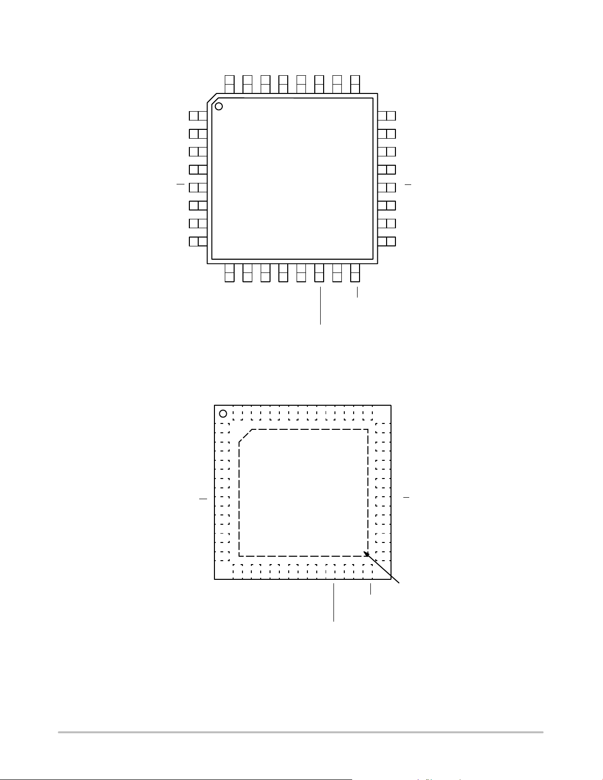
2526272829303132
1
2
3
4
5
6
7
8
VEELEN
MC10EP195
MC100EP195
SETMAX
SETMIN
CC
V
CASCADE
24
23
22
21
20
19
18
17
16
1514131211109
CASCADE
EN
Figure 1. 32−Lead LQFP Pinout (Top View)
V
D0
V
V
V
NC
EE
CC
Q
Q
CC
CC
D8
D9
D10
IN
IN
V
BB
V
EF
V
CF
V
EE
CC
V
D3
CASCADE
D4
D5
D6
D7
32 31 30 29 28 27 26 25
1
2
3
4
5
6
7
8
9 10 1112 1314 1516
VEELEN
SETMAX
SETMIN
Figure 2. 32−Lead QFN (Top View)
D2
D1
CASCADE
EN
24
V
EE
23
D0
22
V
CC
21
Q
20
Q
V
19
CC
V
18
CC
17
NC
Exposed Pad (EP)
http://onsemi.com
2
MC10EP195, MC100EP195
Table 1. PIN DESCRIPTION
Pin Name I/O Default State Description
23, 25, 26, 27,
29, 30, 31, 32,
1, 2
3 D[10] LVCMOS, LVTTL,
4 IN ECL Input Low
5 IN ECL Input High
6 V
7 V
8 V
9, 24, 28 V
13, 18, 19, 22 V
10 LEN ECL Input Low
11 SETMIN ECL Input Low
12 SETMAX ECL Input Low
14 CASCADE ECL Output − Inverted Differential Cascade Output for D[10]. Typically Terminated
15 CASCADE ECL Output − Noninverted Differential Cascade Output. for D[10] Typically
16 EN ECL Input Low
17 NC − − No Connect. The NC Pin is Electrically Connected to the Die and
21 Q ECL Output −
20 Q ECL Output −
1. SETMIN will override SETMAX if both are high. SETMAX and SETMIN will override all D[0:10] inputs.
2. All V
and VEE pins must be externally connected to Power Supply to guarantee proper operation.
CC
D[0:9] LVCMOS, LVTTL,
ECL Input
ECL Input
BB
EF
CF
EE
CC
− − ECL Reference Voltage Output
− − Reference Voltage for ECL Mode Connection
− − LVCMOS, ECL, OR LVTTL Input Mode Select
− − Negative Supply Voltage. All VEE Pins must be Externally
− − Positive Supply Voltage. All VCC Pins must be externally
Low
Low
Single−Ended Parallel Data Inputs [0:9]. Internal 75 kW to VEE.
(Note 1)
Single−Ended CASCADE/CASCADE Control Input. Internal 75 kW
to V
. (Note 1)
EE
Noninverted Differential Input. Internal 75 kW to VEE.
Inverted Differential Input. Internal 75 kW to VEE and 36.5 kW to
V
.
CC
Connected to Power Supply to Guarantee Proper Operation.
(Note 2)
Connected to Power Supply to Guarantee Proper Operation.
(Note 2)
Single−ended D pins LOAD / HOLD input. Internal 75 kW to VEE.
Single−ended Minimum Delay Set Logic Input. Internal 75 kW to
V
. (Note 1)
EE
Single−ended Maximum Delay Set Logic Input. Internal 75 kW to
V
. (Note 1)
EE
with 50 W to V
Terminated with 50 W to V
= VCC − 2 V.
TT
= VCC − 2 V.
TT
Single−ended Output Enable Pin. Internal 75 kW to VEE.
”MUST BE” Left Open
Noninverted Differential Output. Typically Terminated with 50 W to
V
= VCC − 2 V.
TT
Inverted Differential Output. Typically Terminated with 50 W to
VTT = VCC − 2 V.
http://onsemi.com
3
MC10EP195, MC100EP195
Table 2. CONTROL PIN
Pin State Function
EN
LEN
SETMIN
SETMAX
D10
3. Internal pulldown resistor will provide a logic LOW if pin is left unconnected.
Table 3. CONTROL D[0:10] INTERFACE
V
CF
V
CF
V
CF
4. Short VCF (pin 8) and VEF (pin 7).
5. When Operating in LVTTL Mode, the reference voltage can be provided by connecting an external resistor, R
is 2.2 kW $5%), between V
LOW (Note 3) Input Signal is Propagated to the Output
HIGH Output Holds Logic Low State
LOW (Note 3) Transparent or LOAD mode for real time delay values present on D[0:10].
HIGH LOCK and HOLD mode for delay values on D[0:10]; further changes on D[0:10]
LOW (Note 3) Output Delay set by D[0:10]
HIGH Set Minimum Output Delay
LOW (Note 3) Output Delay set by D[0:10]
HIGH Set Maximum Output Delay
LOW (Note 3) CASCADE Output LOW, CASCADE Output HIGH
HIGH CASCADE Output LOW, CASCADE Output HIGH
VEF Pin (Note 4) ECL Mode
No Connect LVCMOS Mode
1.5 V $ 100 mV LVTTL Mode (Note 5)
and VEE pins.
CF
are not recognized and do not affect delay.
(suggested resistor value
CF
Table 4. DATA INPUT ALLOWED OPERATING VOLTAGE MODE TABLE
CONTROL DATA SELECT INPUTS PINS (D [0:10])
POWER SUPPLY
PECL Mode Operating Range YES YES YES N/A
NECL Mode Operating Range N/A N/A N/A YES
LVCMOS LVTTL LVPECL LVNECL
Table 5. ATTRIBUTES
Characteristics Value
Internal Input Pulldown Resistor (R1)
ESD Protection Human Body Model
Machine Model
Charged Device Model
Moisture Sensitivity, Indefinite Time Out of Drypack (Note 6) Pb Pkg Pb−Free Pkg
LQFP−32 Level 2 Level 2
QFN−32 − Level 1
Flammability Rating Oxygen Index: 28 to 34 UL 94 V−0 @ 0.125 in
Transistor Count 1217 Devices
Meets or exceeds JEDEC Spec EIA/JESD78 IC Latchup Test
6. For additional information, see Application Note AND8003/D.
75 kW
> 2 kV
> 100 V
> 2 kV
http://onsemi.com
4
MC10EP195, MC100EP195
Q
Q
0
1
1
GD*
0
1
0
1
1
1
GD*
GD*
0
1
2
GD*
0
1
4
GD*
0
1
8
GD*
R1R1R1R1R1R1R1R1R1R1
D0D1D2D3D4D5D6D7D8D9
0
1
16
GD*
0
1
10 BIT LATCH
(MINIMUM FIXED DELAY APPROX. 2.2 ns)
32
GD*
*GD = (GATE DELAY) APPROXIMATELY 10 ps DELAY PER GATE
0
1
64
GD*
0
1
CASCADE
128
GD*
0
1
256
GD*
0
1
512
GD*
R1
R1
R1
IN
IN
EN
R1
LEN
R1
SET MIN
SET MAX
R1
BBVCFVEF
V
CASCADE
R1
Latch
EE
V
D10
Figure 3. Logic Diagram
http://onsemi.com
5

Table 6. THEORETICAL DELAY VALUES
D(9:0) Value SETMIN SETMAX Programmable Delay*
XXXXXXXXXX H L 0 ps
0000000000 L L 0 ps
0000000001 L L 10 ps
0000000010 L L 20 ps
0000000011 L L 30 ps
0000000100 L L 40 ps
0000000101 L L 50 ps
0000000110 L L 60 ps
0000000111 L L 70 ps
0000001000 L L 80 ps
0000010000 L L 160 ps
0000100000 L L 320 ps
0001000000 L L 640 ps
0010000000 L L 1280 ps
0100000000 L L 2560 ps
1000000000 L L 5120 ps
1111111111 L L 10230 ps
XXXXXXXXXX L H 10240 ps
*Fixed minimum delay not included.
MC10EP195, MC100EP195
http://onsemi.com
6

14000.0
13000.0
12000.0
11000.0
10000.0
9000.0
8000.0
7000.0
6000.0
DELAY ( ps)
5000.0
4000.0
3000.0
2000.0
1000.0
MC10EP195, MC100EP195
85°C
25°C
VCC = 0 V
= −3.3 V
V
EE
0.0
0.0 100.0 200.0 300.0 400.0 500.0 600.0 700.0 800.0 900.0 1000.0
Decimal Value of Select Inputs (D[9:0])
−40°C
Figure 4. Measured Delay vs. Select Inputs
Table 7. MAXIMUM RATINGS
Symbol Parameter Condition 1 Condition 2 Rating Unit
V
CC
V
EE
V
I
I
out
I
BB
T
A
T
stg
q
JA
q
JC
q
JA
q
JC
T
sol
Stresses exceeding Maximum Ratings may damage the device. Maximum Ratings are stress ratings only. Functional operation above the
Recommended Operating Conditions is not implied. Extended exposure to stresses above the Recommended Operating Conditions may affect
device reliability.
Positive Mode Power Supply VEE = 0 V 6 V
Negative Mode Power Supply VCC = 0 V −6 V
Positive Mode Input Voltage
Negative Mode Input Voltage
Output Current Continuous
VEE = 0 V
V
= 0 V
CC
Surge
VI ≤ V
VI ≥ V
CC
EE
6
−6
50
100
V
V
mA
mA
VBB Sink/Source ±0.5 mA
Operating Temperature Range −40 to +85 °C
Storage Temperature Range −65 to +150 °C
Thermal Resistance (Junction−to−Ambient) 0 lfpm
500 lfpm
LQFP−23
LQFP−23
80
55
°C/W
°C/W
Thermal Resistance (Junction−to−Case) Standard Board LQFP−23 12 to 17 °C/W
Thermal Resistance (Junction−to−Ambient) 0 lfpm
500 lfpm
QFN−32
QFN−32
31
27
°C/W
°C/W
Thermal Resistance (Junction−to−Case) 2S2P QFN−32 12 °C/W
Wave Solder Pb
Pb−Free
<2 to 3 sec @ 248°C
<2 to 3 sec @ 260°C
265
265
°C
http://onsemi.com
7

MC10EP195, MC100EP195
Table 8. 10EP DC CHARACTERISTICS, PECL V
= 3.3 V, VEE = 0 V (Note 7)
CC
−40°C 25°C 85°C
Symbol
I
EE
V
OH
V
OL
V
IH
V
IL
V
BB
V
CF
V
EF
V
IHCMR
I
IH
I
IL
Characteristic
Negative Power Supply Current 100 145 175 100 150 180 100 150 180 mA
Output HIGH Voltage (Note 8) 2165 2290 2415 2230 2355 2480 2290 2415 2540 mV
Output LOW Voltage (Note 8) 1365 1490 1615 1430 1555 1680 1490 1615 1740 mV
Input HIGH Voltage (Single−Ended)
LVPECL
LVCMOS
LVTTL
Input LOW Voltage (Single−Ended)
LVPECL
LVCMOS
LVTTL
ECL Output Voltage Reference 1790 1890 1990 1855 1955 2055 1915 2015 2115 mV
LVTTL Mode Input Detect Voltage 1.4 1.5 1.6 1.4 1.5 1.6 1.4 1.5 1.6 V
Reference Voltage for ECL Mode Connection 1900 2020 2150 1875 2080 2150 1850 2130 2150 mV
Input HIGH Voltage Common Mode Range
(Differential Configuration) (Note 9)
Input HIGH Current (@ VIH) 150 150 150
Input LOW Current (@ VIL)IN
Min Typ Max Min Typ Max Min Typ Max
2090
2000
2000
1365
0
0
2415
3300
3300
1690
800
800
2155
2000
2000
1430
0
0
2480
3300
3300
1755
800
800
2215
2000
2000
1490
0
0
2.0 3.3 2.0 3.3 2.0 3.3 V
0.5
−150
IN
0.5
−150
0.5
−150
Unit
2540
3300
3300
1815
800
800
NOTE: Device will meet the specifications after thermal equilibrium has been established when mounted in a test socket or printed circuit
board with maintained transverse airflow greater than 500 lfpm. Electrical parameters are guaranteed only over the declared
operating temperature range. Functional operation of the device exceeding these conditions is not implied. Device specification limit
values are applied individually under normal operating conditions and not valid simultaneously.
7. Input and output parameters vary 1:1 with V
8. All loading with 50 W to V
9. V
min varies 1:1 with VEE, V
IHCMR
input signal.
− 2.0 V.
CC
IHCMR
. VEE can vary +0.3 V to −0.3 V.
CC
max varies 1:1 with VCC. The V
range is referenced to the most positive side of the differential
IHCMR
mV
mV
mA
mA
http://onsemi.com
8

MC10EP195, MC100EP195
Table 9. 10EP DC CHARACTERISTICS, NECL V
= 0 V, V
CC
= −3.3 V to −3.0 V (Note 10)
EE
−40°C 25°C 85°C
Symbol
I
EE
V
OH
V
OL
V
IH
V
IL
V
BB
V
EF
V
IHCMR
Characteristic
Negative Power Supply Current 100 145 175 100 150 180 100 150 180 mA
Output HIGH Voltage (Note 11) −1135 −1010 −885 −1070 −945 −820 −1010 −885 −760 mV
Output LOW Voltage (Note 11) −1935 −1810 −1685 −1870 −1745 −1620 −1810 −1685 −1560 mV
Input HIGH Voltage (Single−Ended)
LVNECL
Input LOW Voltage (Single−Ended)
LVNECL
ECL Output Voltage Reference −1510 −1410 −1310 −1445 −1345 −1245 −1385 −1285 −1185 mV
Reference Voltage for ECL Mode
Connection
Input HIGH Voltage Common Mode
Min Ty p Max Min Typ Max Min Typ Max
Unit
−1210 −885 −1145 −820 −1085 −760
−1935 −1610 −1870 −1545 −1810 −1485
−1400 −1280 −1250 −1425 −1220 −1250 −1450 −1170 −1250 mV
VEE+2.0 0.0 VEE+2.0 0.0 VEE+2.0 0.0 V
Range (Differential Configuration)
(Note 12)
I
IH
I
IL
Input HIGH Current (@ VIH) 150 150 150
Input LOW Current (@ VIL)ININ0.5
−150
0.5
−150
0.5
−150
NOTE: Device will meet the specifications after thermal equilibrium has been established when mounted in a test socket or printed circuit
board with maintained transverse airflow greater than 500 lfpm. Electrical parameters are guaranteed only over the declared
operating temperature range. Functional operation of the device exceeding these conditions is not implied. Device specification limit
values are applied individually under normal operating conditions and not valid simultaneously.
10.Input and output parameters vary 1:1 with V
11.All loading with 50 W to V
12.V
min varies 1:1 with VEE, V
IHCMR
input signal.
CC
− 2.0 V.
IHCMR
max varies 1:1 with VCC. The V
can vary +0.3 V to −0.3 V.
CC. VEE
range is referenced to the most positive side of the differential
IHCMR
mV
mV
mA
mA
http://onsemi.com
9

MC10EP195, MC100EP195
Table 10. 100EP DC CHARACTERISTICS, PECL V
= 3.3 V, VEE = 0 V (Note 13)
CC
−40°C 25°C 85°C
Symbol
I
EE
V
OH
V
OL
V
IH
V
IL
V
BB
V
CF
V
EF
V
IHCMR
I
IH
I
IL
Characteristic
Negative Power Supply Current 100 135 160 100 140 170 100 145 175 mA
Output HIGH Voltage (Note 14) 2155 2280 2405 2155 2280 2405 2155 2280 2405 mV
Output LOW Voltage (Note 14) 1355 1480 1605 1355 1480 1605 1355 1480 1605 mV
Input HIGH Voltage (Single−Ended)
LVPECL
CMOS
Input LOW Voltage (Single−Ended)
LVPECL
CMOS
ECL Output Voltage Reference 1775 1875 1975 1775 1875 1975 1775 1875 1975 mV
LVTTL Mode Input Detect Voltage 1.4 1.5 1.6 1.4 1.5 1.6 1.4 1.5 1.6 V
Reference Voltage for ECL Mode Connection 1900 2020 2150 1875 2080 2150 1850 2130 2150 mV
Input HIGH Voltage Common Mode Range
(Differential Configuration) (Note 15)
Input HIGH Current (@ VIH) 150 150 150
Input LOW Current (@ VIL)IN
Min Typ Max Min Typ Max Min Typ Max
TTL
TTL
2075
2000
2000
1355
0
0
2420
3300
3300
1675
800
800
2075
2000
2000
1490
0
0
2420
3300
3300
1675
800
800
2075
2000
2000
1490
0
0
2.0 3.3 2.0 3.3 2.0 3.3 V
0.5
−150
IN
0.5
−150
0.5
−150
Unit
2420
3300
3300
1675
800
800
NOTE: Device will meet the specifications after thermal equilibrium has been established when mounted in a test socket or printed circuit
board with maintained transverse airflow greater than 500 lfpm. Electrical parameters are guaranteed only over the declared
operating temperature range. Functional operation of the device exceeding these conditions is not implied. Device specification limit
values are applied individually under normal operating conditions and not valid simultaneously.
13.Input and output parameters vary 1:1 with V
14.All loading with 50 W to V
15.V
min varies 1:1 with VEE, V
IHCMR
input signal.
− 2.0 V.
CC
max varies 1:1 with V
IHCMR
can vary +0.3 V to −0.3 V.
CC. VEE
CC.
The V
range is referenced to the most positive side of the differential
IHCMR
mV
mV
mA
mA
http://onsemi.com
10

MC10EP195, MC100EP195
Table 11. 100EP DC CHARACTERISTICS, NECL V
= 0 V, V
CC
= −3.3 V (Note 16)
EE
−40°C 25°C 85°C
Symbol
I
EE
Characteristic
Negative Power Supply Current
Min Ty p Max Min Typ Max Min Ty p Max
Unit
100 135 160 100 140 170 100 145 175 mA
(Note 17)
V
OH
V
OL
V
IH
V
IL
V
BB
V
EF
V
IHCMR
Output HIGH Voltage (Note 18) −1145 −1020 −895 −1145 −1020 −895 −1145 −1020 −895 mV
Output LOW Voltage (Note 18) −1945 −1820 −1695 −1945 −1820 −1695 −1945 −1820 −1695 mV
Input HIGH Voltage (Single−Ended)
LVNECL
−1225 −880 −1225 −880 −1225 −880
Input LOW Voltage (Single−Ended)
LVNECL
−1945 −1625 −1945 −1625 −1945 −1625
ECL Output Voltage Reference −1525 −1425 −1325 −1525 −1425 −1325 −1525 −1425 −1325 mV
Reference Voltage for ECL Mode Con-
−1400 −1280 −1250 −1425 −1220 −1250 −1450 −1170 −1250 mV
nection
Input HIGH Voltage Common Mode
VEE+2.0 0.0 VEE+2.0 0.0 VEE+2.0 0.0 V
Range (Differential Configuration)
(Note 19)
I
IH
I
IL
Input HIGH Current (@ VIH) 150 150 150
Input LOW Current (@ VIL)IN
0.5
−150
IN
0.5
−150
0.5
−150
NOTE: Device will meet the specifications after thermal equilibrium has been established when mounted in a test socket or printed circuit
board with maintained transverse airflow greater than 500 lfpm. Electrical parameters are guaranteed only over the declared
operating temperature range. Functional operation of the device exceeding these conditions is not implied. Device specification limit
values are applied individually under normal operating conditions and not valid simultaneously.
16.Input and output parameters vary 1:1 with V
17.Required 500 lfpm air flow when using +5 V power supply. For (V
protection at elevated temperatures. Recommend V
18.All loading with 50 W to V
19.V
min varies 1:1 with VEE, V
IHCMR
input signal.
CC
− 2.0 V.
IHCMR
max varies 1:1 with VCC. The V
can vary +0.3 V to −0.3 V.
CC. VEE
− VEE operation at ≤ 3.8 V.
CC
− VEE) > 3.3 V, 5 W to 10 W in line with VEE required for maximum thermal
CC
range is referenced to the most positive side of the differential
IHCMR
mV
mV
mA
mA
http://onsemi.com
11

MC10EP195, MC100EP195
Table 12. AC CHARACTERISTICS V
= 0 V; VEE = −3.0 V to −3.6 V or VCC = 3.0 V to 3.6 V; V
CC
= 0 V (Note 20)
EE
−40°C 25°C 85°C
Symbol
f
max
t
PLH
t
PHL
t
RANGE
Dt
Characteristic
Maximum Frequency 1.2 1.2 1.2 GHz
Propagation Delay
IN to Q; D(0−10) = 0
IN to Q; D(0−10) = 1023
to Q; D(0−10) = 0
EN
D0 to CASCADE
Programmable Range
(max) − tPD (min)
t
PD
Step Delay (Note 21)
D0 High
D1 High
D2 High
D3 High
D4 High
D5 High
D6 High
D7 High
D8 High
D9 High
Min Ty p Max Min Typ Max Min Ty p Max
1650
9500
1600
300
2050
11500
2150
420
2450
13500
2600
500
1800
10000
1800
350
2200
12200
2300
450
2600
14000
2800
550
1950
10800
2000
425
2350
13300
2500
525
2750
15800
3000
625
7850 9450 8200 10000 8850 10950
13
27
44
90
130
312
590
1100
2250
4500
14
30
47
97
140
335
650
1180
2400
4800
41
100
145
360
690
1300
2650
5300
Unit
ps
ps
ps
mono Monotonicity (Note 27) TBD
t
SKEW
t
s
t
h
t
R
t
jitter
V
PP
t
r
t
f
Duty Cycle Skew (Note 22)
|t
PHL−tPLH
Setup Time
D to LEN
D to IN (Note 23)
to IN (Note 24)
EN
Hold Time
LEN to D
(Note 25)
IN to EN
Release Time
to IN (Note 26)
EN
SET MAX to LEN
SET MIN to LEN
RMS Random Clock Jitter @ 1.2 GHz
IN to Q; D(0:10) = 0 or SETMIN
IN to Q; D(0:10) = 1023 or SETMAX
Input Voltage Swing
(Differential Configuration)
Output Rise/Fall Time @ 50 MHz
20−80% (Q)
20−80% (CASCADE)
|
200
300
300
200
40060250
150
400
350
25 25 25
0
140
150
−25
200
275
0.86
0.89
200
300
300
200
400
150
400
350
0
160
170
100
280
−75
250
200
1.16
1.09
200
300
300
200
40080300
150
400
350
0
180
180
−50
300
225
1.12
1.02
150 800 1200 150 800 1200 150 800 1200 mV
85
100
100
140
135
20085110
110
150
135
20095130
125
170
155
220
ps
ps
ps
ps
ps
ps
NOTE: Device will meet the specifications after thermal equilibrium has been established when mounted in a test socket or printed circuit
board with maintained transverse airflow greater than 500 lfpm. Electrical parameters are guaranteed only over the declared
operating temperature range. Functional operation of the device exceeding these conditions is not implied. Device specification limit
values are applied individually under normal operating conditions and not valid simultaneously.
20.Measured using a 750 mV source, 50% duty cycle clock source. All loading with 50 W to V
21.Specification limits represent the amount of delay added with the assertion of each individual delay control pin. The various combinations
− 2.0 V.
CC
of asserted delay control inputs will typically realize D0 resolution steps across the specified programmable range.
22.Duty cycle skew guaranteed only for differential operation measured from the cross point of the input to the cross point of the output.
23.This setup time defines the amount of time prior to the input signal the delay tap of the device must be set.
24.This setup time is the minimum time that EN
±75 mV to that IN/IN
transition.
25.This hold time is the minimum time that EN
must be asserted prior to the next transition of IN/IN to prevent an output response greater than
must remain asserted after a negative going IN or positive going IN to prevent an output response
greater than ±75 mV to that IN/IN transition.
26.This release time is the minimum time that EN
must be deasserted prior to the next IN/IN transition to ensure an output response that meets
the specified IN to Q propagation delay and transition times.
27.The monotonicity indicates the increasing delay value for each binary count increment on the control inputs D[9:0].
http://onsemi.com
12

MC10EP195, MC100EP195
IN
V
IN
Q
V
Q
t
PHL
t
PLH
Figure 5. AC Reference Measurement
= VIH(D) − VIL(D)
INPP
= VOH(Q) − VOL(Q)
OUTPP
Cascading Multiple EP195s
To increase the programmable range of the EP195,
internal cascade circuitry has been included. This circuitry
allows for the cascading of multiple EP195s without the
need for any external gating. Furthermore, this capability
requires only one more address line per added E195.
Obviously, cascading multiple programmable delay chips
will result in a larger programmable range: however, this
increase is at the expense of a longer minimum delay.
Need if Chip #3 is used
D3D4D5D6D7
D2 D1
V
EE
D0
V
CC
Q
Q
V
CC
V
CC
INPUT
D8
D9
D10
IN
IN
V
BB
V
EF
V
EP195
CHIP #2
EE
Figure 6 illustrates the interconnect scheme for cascading
two EP195s. As can be seen, this scheme can easily be
expanded for larger EP195 chains. The D10 input of the
EP195 is the CASCADE control pin. With the interconnect
scheme of Figure 6 when D10 is asserted, it signals the need
for a larger programmable range than is achievable with a
single device and switches output pin CASCADE HIGH and
pin CASCADE
LOW. The A11 address can be added to
generate a cascade output for the next EP195. For a 2−device
configuration, A11 is not required.
A11 A10 A9 A8 A7 A6 A5 A4 A3 A2 A1 A0
D8
D9
D10
IN
IN
V
BB
V
EF
ADDRESS BUS
V
EE
EP195
CHIP #1
D3D4D5D6D7
D2 D1
V
EE
D0
V
CC
Q
OUTPUT
Q
V
CC
V
CC
V
CF
VEELEN
SETMAX
SETMIN
CC
V
CASCADE
CASCADE
NC
EN
V
CF
VEELEN
Figure 6. Cascading Interconnect Architecture
http://onsemi.com
13
SETMAX
SETMIN
V
CC
CASCADE
CASCADE
NC
EN

MC10EP195, MC100EP195
An expansion of the latch section of the block diagram is
pictured in Figure 7. Use of this diagram will simplify the
explanation of how the cascade circuitry works. When D10
of chip #1 in Figure 6 is LOW this device’s
CASCADE output will also be low while the CASCADE
output will be high. In this condition the SET MIN pin of
chip #2 will be asserted HIGH and thus all of the latches of
chip #2 will be reset and the device will be set at its minimum
delay.
Chip #1, on the other hand, will have both SET MIN and
SET MAX deasserted so that its delay will be controlled
entirely by the address bus A0—A9. If the delay needed is
greater than can be achieved with 1023 gate delays
TO SELECT MULTIPLEXERS
SET
MIN
SET
MAX
BIT 0
D0 Q0
LEN
Set Reset
BIT 1
D1 Q1
LEN
Set Reset
BIT 2
D2 Q2
LEN
Set Reset
BIT 3
D3 Q3
LEN
Set Reset
BIT 4
D4 Q4
LEN
Set Reset
(1111111111 on the A0—A9 address bus) D10 will be
asserted to signal the need to cascade the delay to the next
EP195 device. When D10 is asserted, the SET MIN pin of
chip #2 will be deasserted and SET MAX pin asserted
resulting in the device delay to be the maximum delay.
Table 13 shows the delay time of two EP195 chips in
cascade.
To expand this cascading scheme to more devices, one
simply needs to connect the D10 pin from the next chip to
the address bus and CASCADE outputs to the next chip in
the same manner as pictured in Figure 6. The only addition
to the logic is the increase of one line to the address bus for
cascade control of the second programmable delay chip.
BIT 5
D5 Q5
LEN
Set Reset
BIT 6
D6 Q6
LEN
Set Reset
BIT 7
D7 Q7
LEN
Set Reset
BIT 8
D8 Q8
LEN
Set Reset
BIT 9
D9 Q9
LEN
Set Reset
Figure 7. Expansion of the Latch Section of the EP195 Block Diagram
http://onsemi.com
14

MC10EP195, MC100EP195
Table 13. Delay Value of Two EP195 Cascaded
VARIABLE INPUT TO CHIP #1 AND SETMIN FOR CHIP #2
INPUT FOR CHIP #1 Total
D10 D9 D8 D7 D6 D5 D4 D3 D2 D1 D0 Delay Value Delay Value
0 0 0 0 0 0 0 0 0 0 0 0 ps 4400 ps
0 0 0 0 0 0 0 0 0 0 1 10 ps 4410 ps
0 0 0 0 0 0 0 0 0 1 0 20 ps 4420 ps
0 0 0 0 0 0 0 0 0 1 1 30 ps 4430 ps
0 0 0 0 0 0 0 0 1 0 0 40 ps 4440 ps
0 0 0 0 0 0 0 0 1 0 1 50 ps 4450 ps
0 0 0 0 0 0 0 0 1 1 0 60 ps 4460 ps
0 0 0 0 0 0 0 0 1 1 1 70 ps 4470 ps
0 0 0 0 0 0 0 1 0 0 0 80 ps 4480 ps
0 0 0 0 0 0 1 0 0 0 0 160 ps 4560 ps
0 0 0 0 0 1 0 0 0 0 0 220 ps 4720 ps
0 0 0 0 1 0 0 0 0 0 0 640 ps 5040 ps
0 0 0 1 0 0 0 0 0 0 0 1280 ps 5680 ps
0 0 1 0 0 0 0 0 0 0 0 2560 ps 6960 ps
0 1 0 0 0 0 0 0 0 0 0 5120 ps 9520 ps
0 1 1 1 1 1 1 1 1 1 1 10230 ps 14630 ps
VARIABLE INPUT TO CHIP #1 AND SETMAX FOR CHIP #2
INPUT FOR CHIP #1 Total
D10 D9 D8 D7 D6 D5 D4 D3 D2 D1 D0 Delay Value Delay Value
1 0 0 0 0 0 0 0 0 0 0 10240 ps 14640 ps
1 0 0 0 0 0 0 0 0 0 1 10250 ps 14650 ps
1 0 0 0 0 0 0 0 0 1 0 10260 ps 14660 ps
1 0 0 0 0 0 0 0 0 1 1 10270 ps 14670 ps
1 0 0 0 0 0 0 0 1 0 0 10280 ps 14680 ps
1 0 0 0 0 0 0 0 1 0 1 10290 ps 14690 ps
1 0 0 0 0 0 0 0 1 1 0 10300 ps 14700 ps
1 0 0 0 0 0 0 0 1 1 1 10310 ps 14710 ps
1 0 0 0 0 0 0 1 0 0 0 10320 ps 14720 ps
1 0 0 0 0 0 1 0 0 0 0 10400 ps 14800 ps
1 0 0 0 0 1 0 0 0 0 0 10560 ps 14960 ps
1 0 0 0 1 0 0 0 0 0 0 10880 ps 15280 ps
1 0 0 1 0 0 0 0 0 0 0 11520 ps 15920 ps
1 0 1 0 0 0 0 0 0 0 0 12800 ps 17200 ps
1 1 0 0 0 0 0 0 0 0 0 15360 ps 19760 ps
1 1 1 1 1 1 1 1 1 1 1 20470 ps 24870 ps
http://onsemi.com
15

MC10EP195, MC100EP195
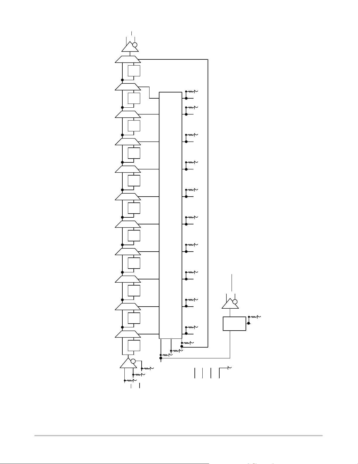
Multi−Channel Deskewing
The most practical application for EP195 is in multiple
channel delay matching. Slight differences in impedance and
cable length can create large timing skews within a high−speed
system. To deskew multiple signal channels, each channel can
IN Q
IN
IN Q
IN
IN Q
IN
Digital
Control
Logic
Data
be sent through each EP195 as shown in Figure 8. One signal
channel can be used as reference and the other EP195s can be
used to adjust the delay to eliminate the timing skews. Nearly
any high−speed system can be fine−tuned (as small as 10 ps)
to reduce the skew to extremely tight tolerances.
EP195
Q
#1
EP195
Q
#2
EP195
Q
#N
Figure 8. Multiple Channel Deskewing Diagram
Measure Unknown High Speed Device Delays
EP195s provide a possible solution to measure the
unknown delay of a device with a high degree of precision.
By combining two EP195s and EP31 as shown in Figure 9,
the delay can be measured. The first EP195 can be set to
SETMIN and its output is used to drive the unknown delay
device, which in turn drives the input of a D flip−flop of
EP31. The second EP195 is triggered along with the first
EP195 and its output provides a clock signal for EP31.
The programmed delay of the second EP195 is varied to
detect the output edge from the unknown delay device.
CLOCK
CLOCK
IN Q
IN
IN Q
IN
EP195
Q
#1
EP195
Q
#2
If the programmed delay through the second EP195 is too
long, the flip−flop output will be at logic high. On the other
hand, if the programmed delay through the second EP195 is
too short, the flip−flop output will be at a logic low. If the
programmed delay is correctly fine−tuned in the second
EP195, the flip−flop will bounce between logic high and logic
low. The digital code in the second EP195 can be directly
correlated into an accurate device delay.
Unknown Delay
Device
D
EP31
CLK
Q
Q
Control
Logic
Figure 9. Multiple Channel Deskewing Diagram
http://onsemi.com
16

MC10EP195, MC100EP195
Zo = 50 W
Zo = 50 W
50 W 50 W
V
VTT = VCC − 2.0 V
TT
Receiver
Device
Driver
Device
QD
Q D
Figure 10. Typical Termination for Output Driver and Device Evaluation
(See Application Note AND8020/D − Termination of ECL Logic Devices.)
ORDERING INFORMATION
Device Package Shipping
MC10EP195FA LQFP−32 250 Units / Tray
MC10EP195FAG LQFP−32
(Pb−Free)
MC10EP195FAR2 LQFP−32 2000 / Tape & Reel
MC10EP195FAR2G LQFP−32
(Pb−Free)
MC10EP195MNG QFN−32
(Pb−Free)
MC10EP195MNR4G QFN−32
(Pb−Free)
MC100EP195FA LQFP−32 250 Units / Tray
MC100EP195FAG LQFP−32
(Pb−Free)
MC100EP195FAR2 LQFP−32 2000 / Tape & Reel
MC100EP195FAR2G LQFP−32
(Pb−Free)
MC100EP195MNG QFN−32
(Pb−Free)
MC100EP195MNR4G QFN−32
(Pb−Free)
†For information on tape and reel specifications, including part orientation and tape sizes, please refer to our Tape and Reel Packaging
Specifications Brochure, BRD8011/D.
250 Units / Tray
2000 / Tape & Reel
74 Units / Rail
1000 / Tape & Reel
250 Units / Tray
2000 / Tape & Reel
74 Units / Rail
1000 / Tape & Reel
†
http://onsemi.com
17

MC10EP195, MC100EP195
Resource Reference of Application Notes
AN1405/D − ECL Clock Distribution Techniques
AN1406/D − Designing with PECL (ECL at +5.0 V)
AN1503/D −
AN1504/D − Metastability and the ECLinPS Family
AN1568/D − Interfacing Between LVDS and ECL
AN1672/D − The ECL Translator Guide
AND8001/D − Odd Number Counters Design
AND8002/D − Marking and Date Codes
AND8020/D − Termination of ECL Logic Devices
AND8066/D − Interfacing with ECLinPS
AND8090/D − AC Characteristics of ECL Devices
ECLinPSt I/O SPiCE Modeling Kit
http://onsemi.com
18

MC10EP195, MC100EP195
PACKAGE DIMENSIONS
32 LEAD LQFP
CASE 873A−02
ISSUE C
SEATING
PLANE
9
−T−
B1
−AB−
−AC−
A
A1
32
1
4X
25
−U−
T−U0.20 (0.008) ZAB
P
−T−, −U−, −Z−
AE
VB
AE
DETAIL Y
8
9
−Z−
S1
V1
17
4X
T−U0.20 (0.008) ZAC
DETAIL Y
BASE
METAL
N
T−U
M
DF
S
_
8X
M
G
DETAIL AD
E
C
R
J
SECTION AE−AE
0.20 (0.008) ZAC
0.10 (0.004) AC
H
W
_
Q
K
X
NOTES:
1. DIMENSIONING AND TOLERANCING
PER ANSI Y14.5M, 1982.
2. CONTROLLING DIMENSION:
MILLIMETER.
3. DATUM PLANE −AB− IS LOCATED AT
BOTTOM OF LEAD AND IS COINCIDENT
WITH THE LEAD WHERE THE LEAD
EXITS THE PLASTIC BODY AT THE
BOTTOM OF THE PARTING LINE.
4. DATUMS −T−, −U−, AND −Z− TO BE
DETERMINED AT DATUM PLANE −AB−.
5. DIMENSIONS S AND V TO BE
DETERMINED AT SEATING PLANE −AC−.
6. DIMENSIONS A AND B DO NOT INCLUDE
MOLD PROTRUSION. ALLOWABLE
PROTRUSION IS 0.250 (0.010) PER SIDE.
DIMENSIONS A AND B DO INCLUDE
MOLD MISMATCH AND ARE
DETERMINED AT DATUM PLANE −AB−.
7. DIMENSION D DOES NOT INCLUDE
DAMBAR PROTRUSION. DAMBAR
PROTRUSION SHALL NOT CAUSE THE
D DIMENSION TO EXCEED 0.520 (0.020).
8. MINIMUM SOLDER PLATE THICKNESS
SHALL BE 0.0076 (0.0003).
9. EXACT SHAPE OF EACH CORNER MAY
VARY FROM DEPICTION.
DETAIL AD
MILLIMETERS
DIMAMIN MAX MIN MAX
7.000 BSC 0.276 BSC
A1 3.500 BSC 0.138 BSC
B 7.000 BSC 0.276 BSC
B1 3.500 BSC 0.138 BSC
C 1.400 1.600 0.055 0.063
D 0.300 0.450 0.012 0.018
E 1.350 1.450 0.053 0.057
F 0.300 0.400 0.012 0.016
G 0.800 BSC 0.031 BSC
H 0.050 0.150 0.002 0.006
J 0.090 0.200 0.004 0.008
K 0.450 0.750 0.018 0.030
__
M 12 REF 12 REF
N 0.090 0.160 0.004 0.006
P 0.400 BSC 0.016 BSC
Q 1 5 1 5
____
R 0.150 0.250 0.006 0.010
S 9.000 BSC 0.354 BSC
S1 4.500 BSC 0.177 BSC
V 9.000 BSC 0.354 BSC
V1 4.500 BSC 0.177 BSC
W 0.200 REF 0.008 REF
X 1.000 REF 0.039 REF
INCHES
0.250 (0.010)
GAUGE PLANE
http://onsemi.com
19

MC10EP195, MC100EP195
PACKAGE DIMENSIONS
QFN32 5*5*1 0.5 P
CASE 488AM−01
ISSUE O
2 X
32 X
LOCATION
0.15 C
2 X
0.10 C
0.08 C
PIN ONE
0.15
32 X
L
32 X
0.05
C
SIDE VIEW
9
8
1
32
b
A0.10 B
C
C
D
TOP VIEW
D2
(A3)
A1
16
17
24
25
A
B
E
EXPOSED PAD
K
32 X
E2
e
NOTES:
1. DIMENSIONS AND TOLERANCING PER
ASME Y14.5M, 1994.
2. CONTROLLING DIMENSION: MILLIMETERS.
3. DIMENSION b APPLIES TO PLATED
TERMINAL AND IS MEASURED BETWEEN
0.25 AND 0.30 MM TERMINAL
4. COPLANARITY APPLIES TO THE EXPOSED
PAD AS WELL AS THE TERMINALS.
MILLIMETERS
DIM MIN NOM MAX
A 0.800 0.900 1.000
A1 0.000 0.025 0.050
A3 0.200 REF
b 0.180 0.250 0.300
D 5.00 BSC
D2 2.950 3.100 3.250
E 5.00 BSC
E2
2.950 3.100 3.250
A
SEATING
PLANE
e 0.500 BSC
K 0.200 −−− −−−
L 0.300 0.400 0.500
C
SOLDERING FOOTPRINT*
5.30
3.20
32 X
0.63
3.20
5.30
BOTTOM VIEW
32 X
0.28
DIMENSIONS: MILLIMETERS
28 X
0.50 PITCH
*For additional information on our Pb−Free strategy and soldering
details, please download the ON Semiconductor Soldering and
Mounting Techniques Reference Manual, SOLDERRM/D.
ECLinPS is a trademark of Semiconductor Components Industries, LLC.
ON Semiconductor and are registered trademarks of Semiconductor Components Industries, LLC (SCILLC). SCILLC reserves the right to make changes without further notice
to any products herein. SCILLC makes no warranty, representation or guarantee regarding the suitability of its products for any particular purpose, nor does SCILLC assume any liability
arising out of the application or use of any product or circuit, and specifically disclaims any and all liability, including without limitation special, consequential or incidental damages.
“Typical” parameters which may be provided in SCILLC data sheets and/or specifications can and do vary in different applications and actual performance may vary over time. All
operating parameters, including “Typicals” must be validated for each customer application by customer’s technical experts. SCILLC does not convey any license under its patent rights
nor the rights of others. SCILLC products are not designed, intended, or authorized for use as components in systems intended for surgical implant into the body, or other applications
intended to support or sustain life, or for any other application in which the failure of the SCILLC product could create a situation where personal injury or death may occur. Should
Buyer purchase or use SCILLC products for any such unintended or unauthorized application, Buyer shall indemnify and hold SCILLC and its officers, employees, subsidiaries, affiliates,
and distributors harmless against all claims, costs, damages, and expenses, and reasonable attorney fees arising out of, directly or indirectly, any claim of personal injury or death
associated with such unintended or unauthorized use, even if such claim alleges that SCILLC was negligent regarding the design or manufacture of the part. SCILLC is an Equal
Opportunity/Affirmative Action Employer. This literature is subject to all applicable copyright laws and is not for resale in any manner.
PUBLICATION ORDERING INFORMATION
LITERATURE FULFILLMENT:
Literature Distribution Center for ON Semiconductor
P.O. Box 5163, Denver, Colorado 80217 USA
Phone: 303−675−2175 or 800−344−3860 Toll Free USA/Canada
Fax: 303−675−2176 or 800−344−3867 Toll Free USA/Canada
Email: orderlit@onsemi.com
N. American Technical Support: 800−282−9855 Toll Free
USA/Canada
Europe, Middle East and Africa Technical Support:
Phone: 421 33 790 2910
Japan Customer Focus Center
Phone: 81−3−5773−3850
http://onsemi.com
ON Semiconductor Website: www.onsemi.com
Order Literature: http://www.onsemi.com/orderlit
For additional information, please contact your local
Sales Representative
MC10EP195/D
20
 Loading...