

Page 1
MC10ELT22, MC100ELT22
5VDual TTL to Differential
PECL Translator
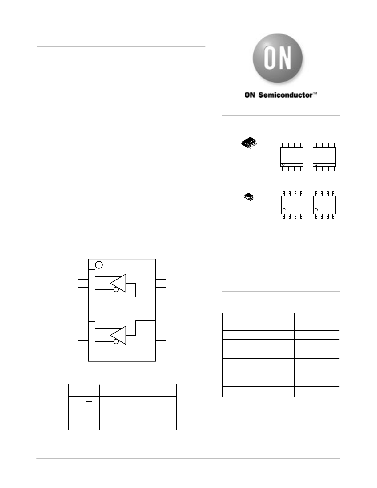
The MC10ELT/100ELT22 is a dual TTL to differential PECL
translator. Because PECL (Positive ECL) levels are used only +5 V
and ground are required. The small outline 8-lead package and the low
skew, dual gate design of the ELT22 makes it ideal for applications
which require the translation of a clock and a data signal.
• 1.2 ns Typical Propagation Delay
• <300 ps Typical Output to Output Skew
• PNP TTL Inputs for Minimal Loading
• Flow Through Pinouts
• ESD Protection: >2 KV HBM, >200 V MM
• Operating Range: V
• No Internal Input Pulldown Resistors
• Meets or Exceeds JEDEC Spec EIA/JESD78 IC Latchup Test
• Moisture Sensitivity Level 1
For Additional Information, see Application Note AND8003/D
• Flammability Rating: UL–94 code V–0 @ 1/8”,
Oxygen Index 28 to 34
• Transistor Count = 51 devices
LOGIC DIAGRAM AND PINOUT ASSIGNMENT
= 4.75 V to 5.25 V with GND= 0 V
CC
http://onsemi.com
8
1
SO–8
D SUFFIX
CASE 751
8
1
TSSOP–8
DT SUFFIX
CASE 948R
H = MC10
K = MC100
A = Assembly Location
DIAGRAMS*
8
HLT22
ALYW
1
8
HT22
ALYW
1
L = Wafer Lot
Y = Year
W = Work Week
MARKING
8
KLT22
ALYW
1
8
KT22
ALYW
1
Q0
Q0
1
2
V
78D0
CC
PECL TTL
3
45
Q1
PIN DESCRIPTION
PIN FUNCTION
Qn, Qn PECL Differential Outputs*
Dn TTL Inputs
V
CC
GND Ground
* Output state undetermined when inputs are open.
Positive Supply
6
D1Q1
GND
*For additional information, see Application Note
AND8002/D
ORDERING INFORMATION
Device Package Shipping
MC10EL T22D SO–8 98 Units/Rail
MC10ELT22DR2 SO–8 2500 Tape & Reel
MC100ELT22D SO–8 98 Units/Rail
MC100ELT22DR2 SO–8 2500 Tape & Reel
MC10ELT22DT TSSOP–8 98 Units/Rail
MC10ELT22DTR2 TSSOP–8 2500 Tape & Reel
MC100ELT22DT TSSOP–8 98 Units/Rail
MC100ELT22DTR2 TSSOP–8 2500 Tape & Reel
Semiconductor Components Industries, LLC, 2000
October, 2000 – Rev. 4
1 Publication Order Number:
MC10ELT22/D
Page 2
MC10ELT22, MC100ELT22
MAXIMUM RATINGS (Note 1.)
Symbol
V
CC
V
IN
I
out
Positive Power Supply GND = 0 V 7 V
Input Voltage GND = 0 V VI V
Output Current Continuous
TA Operating Temperature Range –40 to +85 °C
T
stg
θ
JA
θ
JC
θ
JA
θ
JC
T
sol
Storage Temperature Range –65 to +150 °C
Thermal Resistance (Junction to Ambient) 0 LFPM
Thermal Resistance (Junction to Case) std bd 8 SOIC 41 to 44 °C/W
Thermal Resistance (Junction to Ambient) 0 LFPM
Thermal Resistance (Junction to Case) std bd 8 TSSOP 41 to 44 ± 5% °C/W
Wave Solder <2 to 3 sec @ 248°C 265 °C
1. Maximum Ratings are those values beyond which device damage may occur.
Parameter Condition 1 Condition 2 Rating Units
CC
7 V
50
Surge
500 LFPM
500 LFPM
8 SOIC
8 SOIC
8 TSSOP
8 TSSOP
100
190
130
185
140
mA
mA
°C/W
°C/W
°C/W
°C/W
10ELT SERIES PECL DC CHARACTERISTICS V
= 5.0 V; GND = 0.0 V (Note 1.)
CC
–40°C 25°C 85°C
Symbol Characteristic Min Typ Max Min Typ Max Min Typ Max Unit
I
CC
V
OH
V
OL
Power Supply Current 22 22 22 mA
Output HIGH Voltage (Note 2.) 3920 4010 4110 4020 4105 4190 4090 4185 4280 mV
Output LOW Voltage (Note 2.) 3050 3200 3350 3050 3210 3370 3050 3227 3405 mV
NOTE: Devices are designed to meet the DC specifications shown in the above table, after thermal equilibrium has been established. The
circuit is in a test socket or mounted on a printed circuit board and transverse air flow greater than 500 lfpm is maintained.
1. Output parameters vary 1:1 with V
2. Outputs are terminated through a 50 ohm resistor to V
100ELT SERIES PECL DC CHARACTERISTICS V
. VCC can vary ± 0.25 V.
CC
–2 volts.
CC
= 5.0 V; GND = 0.0 V (Note 1.)
CC
–40°C 25°C 85°C
Symbol Characteristic Min Typ Max Min Typ Max Min Typ Max Unit
I
CC
V
OH
V
OL
Power Supply Current 22 22 22 mA
Output HIGH Voltage (Note 2.) 3915 3995 4120 3975 4045 4120 3975 4050 4120 mV
Output LOW Voltage (Note 2.) 3170 3305 3445 3190 3295 3380 3190 3295 3380 mV
NOTE: Devices are designed to meet the DC specifications shown in the above table, after thermal equilibrium has been established. The
circuit is in a test socket or mounted on a printed circuit board and transverse air flow greater than 500 lfpm is maintained.
1. Output parameters vary 1:1 with V
2. Outputs are terminated through a 50 ohm resistor to V
. VCC can vary ± 0.25 V.
CC
–2 volts.
CC
http://onsemi.com
2
Page 3
MC10ELT22, MC100ELT22
TTL INPUT DC CHARACTERISTICS V
Symbol
I
I
I
V
V
V
IH
IHH
IL
IK
IH
IL
Input HIGH Current VIN = 2.7 V 20 µA
Input HIGH Current VIN = 7.0 V 100 µA
Input LOW Current VIN = 0.5 V –0.6 mA
Input Clamp Diode Voltage IIN = –18 mA –1.2 V
Input HIGH Voltage 2.0 V
Input LOW Voltage 0.8 V
AC CHARACTERISTICS V
Characteristic Condition Min Typ Max Unit
= 4.75 V to 5.25 V; GND= 0.0 V
CC
= 4.75 V to 5.25 V; TA = –40°C to 85°C
CC
–40°C 25°C 85°C
Symbol Characteristic Min Typ Max Min Typ Max Min Typ Max Unit
f
MAX
t
PLH
Maximum Input Frequency 100 100 100 MHz
Propagation Delay (Note 1.)
0.6 1.2 0.9 1.2 1.5 0.6 1.35 ns
1.5 V to 50%
t
PHL
Propagation Delay (Note 1.)
0.4 1.0 0.5 0.8 1.1 0.7 1.30 ns
1.5 V to 50%
t
JITTER
tr/t
f
Cycle–to–Cycle Jitter TBD TBD TBD ps
Output Rise/Fall Time
0.4 1.6 0.4 1.6 0.4 1.6 ns
(20–80%)
1. Specifications for standard TTL input signal.
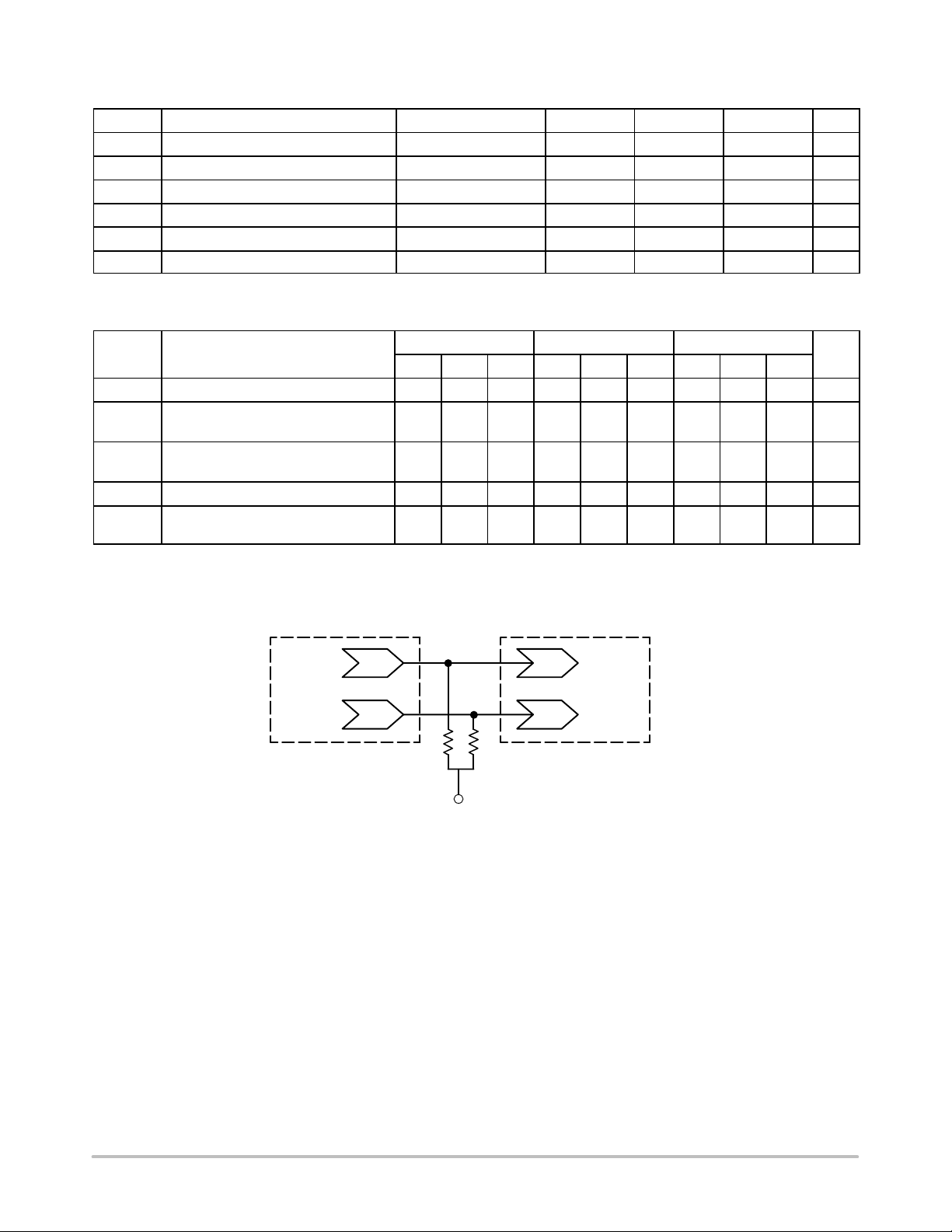
Driver
Device
Q
Qb
50
V
TT
50
V
TT
V
=
CC
– 2.0 V
D
Receiver
Device
Db
Figure 1. Typical Termination for Output Driver and Device Evaluation
(See Application Note AND8020 – Termination of ECL Logic Devices.)
http://onsemi.com
3
Page 4

MC10ELT22, MC100ELT22
Resource Reference of Application Notes
AN1400
AN1404
AN1405
AN1406
AN1503
AN1504
AN1560
AN1568
AN1596
AN1650
AN1672
AND8001
AND8002
AND8020
MC10/100H640 Clock Driver Family I/O SPICE Modeling Kit
–
ECLinPS Circuit Performance at Non–Standard VIH Levels
–
ECL Clock Distribution Techniques
–
Designing with PECL (ECL at +5.0 V)
–
ECLinPS I/O SPICE Modeling Kit
–
Metastability and the ECLinPS Family
–
Low Voltage ECLinPS SPICE Modeling Kit
–
Interfacing Between LVDS and ECL
–
ECLinPS Lite Translator ELT Family SPICE I/O Model Kit
–
Using Wire–OR Ties in ECLinPS Designs
–
The ECL Translator Guide
–
Odd Number Counters Design
–
Marking and Date Codes
–
Termination of ECL Logic Devices
–
http://onsemi.com
4
Page 5

–Y–
–Z–
MC10ELT22, MC100ELT22
PACKAGE DIMENSIONS
SO–8
D SUFFIX
PLASTIC SOIC PACKAGE
CASE 751–07
–X–
A
58
B
1
S
0.25 (0.010)
4
G
C
SEATING
PLANE
0.10 (0.004)
H
D
0.25 (0.010) Z
M
Y
SXS
ISSUE V
NOTES:
1. DIMENSIONING AND TOLERANCING PER ANSI
Y14.5M, 1982.
2. CONTROLLING DIMENSION: MILLIMETER.
3. DIMENSION A AND B DO NOT INCLUDE MOLD
PROTRUSION.
M
M
Y
K
N
X 45
M
4. MAXIMUM MOLD PROTRUSION 0.15 (0.006) PER
SIDE.
5. DIMENSION D DOES NOT INCLUDE DAMBAR
PROTRUSION. ALLOWABLE DAMBAR
PROTRUSION SHALL BE 0.127 (0.005) TOTAL IN
EXCESS OF THE D DIMENSION AT MAXIMUM
MATERIAL CONDITION.
MILLIMETERS
DIMAMIN MAX MIN MAX
4.80 5.00 0.189 0.197
B 3.80 4.00 0.150 0.157
C 1.35 1.75 0.053 0.069
D 0.33 0.51 0.013 0.020
G 1.27 BSC 0.050 BSC
H 0.10 0.25 0.004 0.010
J
J 0.19 0.25 0.007 0.010
K 0.40 1.27 0.016 0.050
M 0 8 0 8
N 0.25 0.50 0.010 0.020
S 5.80 6.20 0.228 0.244
INCHES
http://onsemi.com
5
Page 6

0.10 (0.004)
–T–
SEATING
PLANE
MC10ELT22, MC100ELT22
PACKAGE DIMENSIONS
TSSOP–8
DT SUFFIX
PLASTIC TSSOP PACKAGE
CASE 948R–02
ISSUE A
8x REFK
S
U0.15 (0.006) T
2X L/2
85
L
PIN 1
IDENT
S
U0.15 (0.006) T
0.10 (0.004) V
1
–U–
4
A
M
B
–V–
S
U
T
S
0.25 (0.010)
M
F
DETAIL E
C
D
G
DETAIL E
NOTES:
1. DIMENSIONING AND TOLERANCING PER ANSI
Y14.5M, 1982.
2. CONTROLLING DIMENSION: MILLIMETER.
3. DIMENSION A DOES NOT INCLUDE MOLD
FLASH. PROTRUSIONS OR GATE BURRS. MOLD
FLASH OR GATE BURRS SHALL NOT EXCEED
0.15 (0.006) PER SIDE.
4. DIMENSION B DOES NOT INCLUDE
INTERLEAD FLASH OR PROTRUSION.
INTERLEAD FLASH OR PROTRUSION SHALL NOT
EXCEED 0.25 (0.010) PER SIDE.
5. TERMINAL NUMBERS ARE SHOWN FOR
REFERENCE ONLY.
6. DIMENSION A AND B ARE TO BE
DETERMINED AT DATUM PLANE -W-.
DIM MIN MAX MIN MAX
A 2.90 3.10 0.114 0.122
B 2.90 3.10 0.114 0.122
C 0.80 1.10 0.031 0.043
–W–
D 0.05 0.15 0.002 0.006
F 0.40 0.70 0.016 0.028
G 0.65 BSC 0.026 BSC
K 0.25 0.40 0.010 0.016
L 4.90 BSC 0.193 BSC
M 0 6 0 6
INCHESMILLIMETERS
http://onsemi.com
6
Page 7

Notes
MC10ELT22, MC100ELT22
http://onsemi.com
7
Page 8

MC10ELT22, MC100ELT22
ON Semiconductor and are trademarks of Semiconductor Components Industries, LLC (SCILLC). SCILLC reserves the right to make changes
without further notice to any products herein. SCILLC makes no warranty, representation or guarantee regarding the suitability of its products for any particular
purpose, nor does SCILLC assume any liability arising out of the application or use of any product or circuit, and specifically disclaims any and all liability,
including without limitation special, consequential or incidental damages. “Typical” parameters which may be provided in SCILLC data sheets and/or
specifications can and do vary in different applications and actual performance may vary over time. All operating parameters, including “Typicals” must be
validated for each customer application by customer’s technical experts. SCILLC does not convey any license under its patent rights nor the rights of others.
SCILLC products are not designed, intended, or authorized for use as components in systems intended for surgical implant into the body, or other applications
intended to support or sustain life, or for any other application in which the failure of the SCILLC product could create a situation where personal injury or
death may occur. Should Buyer purchase or use SCILLC products for any such unintended or unauthorized application, Buyer shall indemnify and hold
SCILLC and its officers, employees, subsidiaries, affiliates, and distributors harmless against all claims, costs, damages, and expenses, and reasonable
attorney fees arising out of, directly or indirectly, any claim of personal injury or death associated with such unintended or unauthorized use, even if such claim
alleges that SCILLC was negligent regarding the design or manufacture of the part. SCILLC is an Equal Opportunity/Affirmative Action Employer.
PUBLICATION ORDERING INFORMATION
NORTH AMERICA Literature Fulfillment:
Literature Distribution Center for ON Semiconductor
P.O. Box 5163, Denver, Colorado 80217 USA
Phone: 303–675–2175 or 800–344–3860 Toll Free USA/Canada
Fax: 303–675–2176 or 800–344–3867 Toll Free USA/Canada
Email: ONlit@hibbertco.com
Fax Response Line: 303–675–2167 or 800–344–3810 Toll Free USA/Canada
N. American Technical Support: 800–282–9855 Toll Free USA/Canada
EUROPE: LDC for ON Semiconductor – European Support
German Phone: (+1) 303–308–7140 (Mon–Fri 2:30pm to 7:00pm CET)
Email: ONlit–german@hibbertco.com
French Phone: (+1) 303–308–7141 (Mon–Fri 2:00pm to 7:00pm CET)
Email: ONlit–french@hibbertco.com
English Phone: (+1) 303–308–7142 (Mon–Fri 12:00pm to 5:00pm GMT)
Email: ONlit@hibbertco.com
EUROPEAN TOLL–FREE ACCESS*: 00–800–4422–3781
*Available from Germany, France, Italy, UK, Ireland
CENTRAL/SOUTH AMERICA:
Spanish Phone: 303–308–7143 (Mon–Fri 8:00am to 5:00pm MST)
Email: ONlit–spanish@hibbertco.com
Toll–Free from Mexico: Dial 01–800–288–2872 for Access –
then Dial 866–297–9322
ASIA/PACIFIC: LDC for ON Semiconductor – Asia Support
Phone: 303–675–2121 (Tue–Fri 9:00am to 1:00pm, Hong Kong Time)
Toll Free from Hong Kong & Singapore:
001–800–4422–3781
Email: ONlit–asia@hibbertco.com
JAPAN: ON Semiconductor, Japan Customer Focus Center
4–32–1 Nishi–Gotanda, Shinagawa–ku, Tokyo, Japan 141–0031
Phone: 81–3–5740–2700
Email: r14525@onsemi.com
ON Semiconductor Website: http://onsemi.com
For additional information, please contact your local
Sales Representative.
http://onsemi.com
8
MC10ELT22/D
Page 9

WWW.ALLDATASHEET.COM
Copyright © Each Manufacturing Company.
All Datasheets cannot be modified without permission.
This datasheet has been download from :
www.AllDataSheet.com
100% Free DataSheet Search Site.
Free Download.
No Register.
Fast Search System.
www.AllDataSheet.com
 Loading...