

查询MC100E157FNG供应商
MC10E157, MC100E157
5 VECL Quad 2:1
Multiplexer
Description
The MC10E/100E157 contains four 2:1 multiplexers with
differential outputs. The output data are controlled by the individual
Select (SEL) inputs. The individual select control makes the devices
well suited for random logic designs.
The 100 Series contains temperature compensation.
Features
• Individual Select Controls
• 550 ps Max. D to Output
• 800 ps Max. SEL to Output
• PECL Mode Operating Range: V
with VEE = 0 V
• NECL Mode Operating Range: V
with VEE = −4.2 V to −5.7 V
• Internal Input 50 kW Pulldown Resistors
• ESD Protection: Human Body Model; > 2 kV,
Machine Model; > 200 V
Charged Device Model; > 2 kV
• Meets or Exceeds JEDEC Standard EIA/JESD78 IC Latchup Test
• Moisture Sensitivity Level:
Pb = 1
Pb−Free = 3
For Additional Information, see Application Note AND8003/D
• Flammability Rating: UL 94 V−0 @ 0.125 in,
Oxygen Index: 28 to 34
• Meets or Exceeds JEDEC Spec EIA/JESD78 IC Latchup Test
• Transistor Count = 137 devices
• Pb−Free Packages are Available*
= 4.2 V to 5.7 V
CC
= 0 V
CC
http://onsemi.com
PLCC−28
FN SUFFIX
CASE 776
MARKING DIAGRAM*
1
MCxxxE157FNG
AWLYYWW
xxx = 10 or 100
A = Assembly Location
WL = Wafer Lot
YY = Year
WW = Work Week
G = Pb−Free Package
*For additional information on our Pb−Free strategy and soldering details, please
download the ON Semiconductor Soldering and Mounting Techniques
Reference Manual, SOLDERRM/D.
© Semiconductor Components Industries, LLC, 2006
November, 2006 − Rev. 9
1 Publication Order Number:
*For additional marking information, refer to
Application Note AND8002/D.
ORDERING INFORMATION
See detailed ordering and shipping information in the package
dimensions section on page 6 of this data sheet.
MC10E157/D
D2b
D
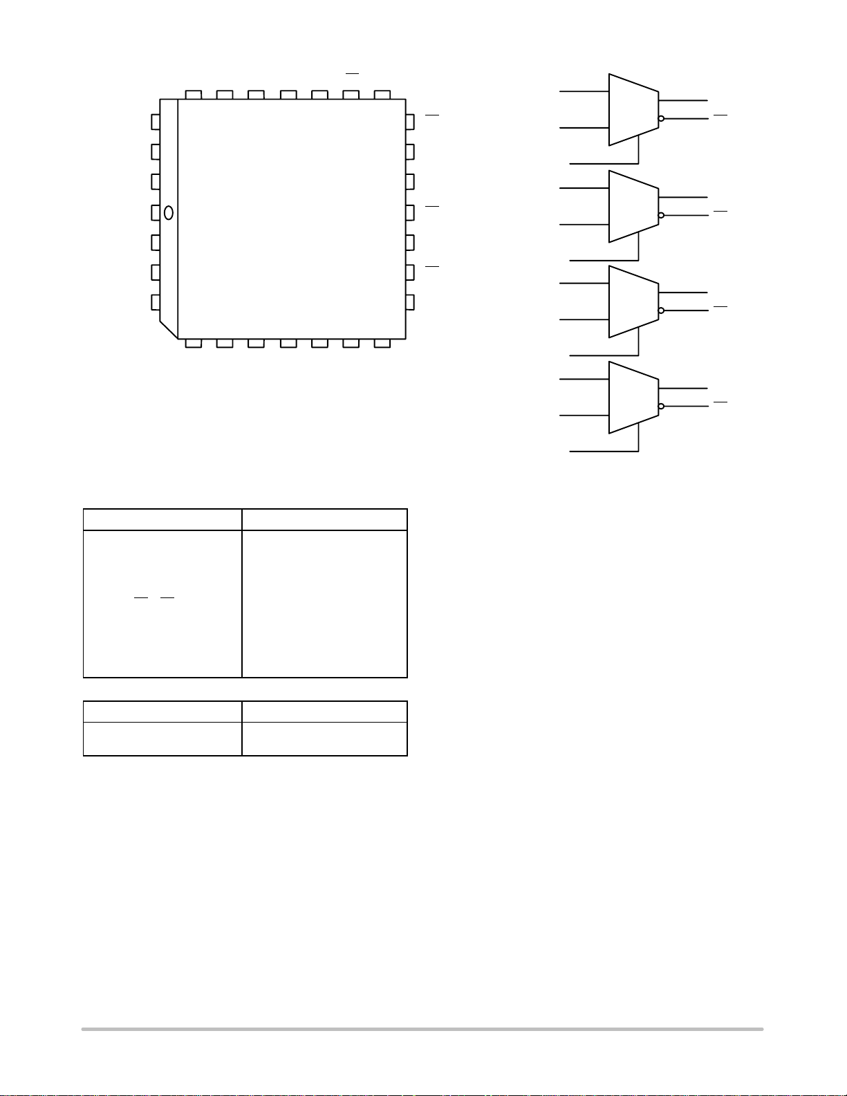
2
SEL2
V
EE
SEL1
D1a
D1b
MC10E157, MC100E157
Q
V
D3bD3aNCSEL3
CCO
25 24 23 22 21 20 19
26
a
27
28
1
Pinout: 28-Lead PLCC
(Top View)
2
3
4
Q
3
3
Q
18
17
2
Q
2
D0a
D0b
1
MUX
0
Q
0
Q
0
SEL0
16
V
CC
15
Q
1
14
Q
1
D1a
D1b
1
0
MUX
Q
1
Q
1
SEL1
13
Q
0
D2a
Q
12
115678910
0
D2b
1
0
MUX
Q
2
Q
2
SEL0 D0aD0bNCNC
* All VCC and V
Warning: All VCC, V
CCO
CCO
NC V
pins are tied together on the die.
, and VEE pins must be externally
connected to Power Supply to guarantee proper operation.
Figure 1. 28−Lead Pinout
Table 1. PIN DESCRIPTION
PIN FUNCTION
D0a − D3a ECL Input Data a
D0b − D3b ECL Input Data b
SEL0 − SEL3 ECL Select Inputs
EE
Q0− Q
3,
CCO
3
ECL Differential Outputs
Positive Supply
Negative Supply
Q0− Q
VCC, V
V
NC No Connect
Table 2. Logic Diagram
SEL Data
H
L
a
b
CCO
SEL2
D3a
1
MUX
D3b
0
SEL3
Figure 2. Logic Diagram
Q
3
Q
3
http://onsemi.com
2
MC10E157, MC100E157
Table 3. MAXIMUM RATINGS
Symbol Parameter Condition 1 Condition 2 Rating Unit
V
CC
V
I
I
out
T
A
T
stg
q
JA
q
JC
T
sol
Stresses exceeding Maximum Ratings may damage the device. Maximum Ratings are stress ratings only. Functional operation above the
Recommended Operating Conditions is not implied. Extended exposure to stresses above the Recommended Operating Conditions may affect
device reliability.
PECL Mode Power Supply VEE = 0 V 8 V
PECL Mode Input Voltage
NECL Mode Input Voltage
Output Current Continuous
VEE = 0 V
VCC = 0 V
Surge
VI v V
VI w V
CC
EE
6
−6
50
100
V
V
mA
mA
Operating Temperature Range 0 to +85 °C
Storage Temperature Range −65 to +150 °C
Thermal Resistance (Junction−to−Ambient) 0 lfpm
500 lfpm
PLCC−28
PLCC−28
63.5
43.5
°C/W
°C/W
Thermal Resistance (Junction−to−Case) Standard Board PLCC−28 22 to 26 °C/W
Wave Solder Pb
Pb−Free
265
265
°C
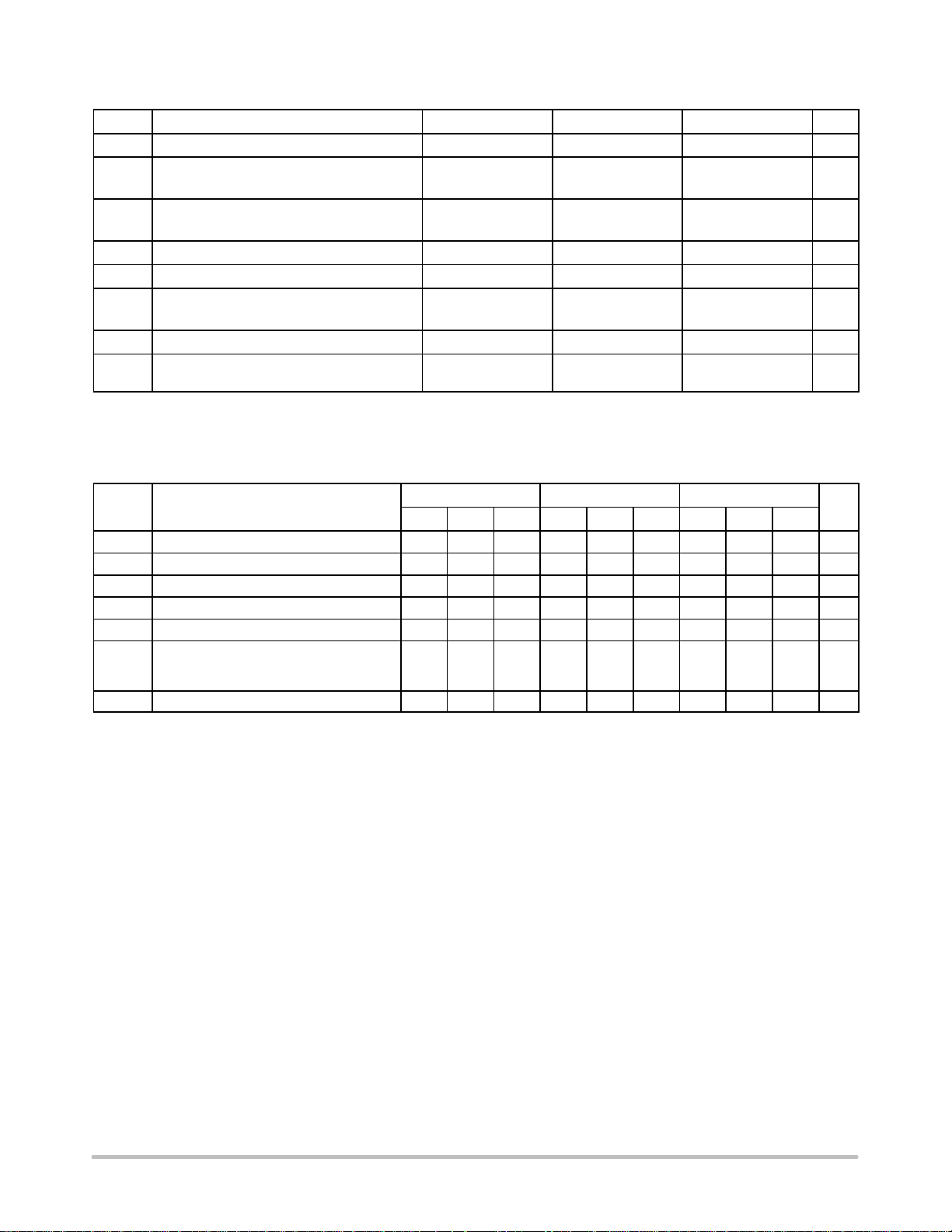
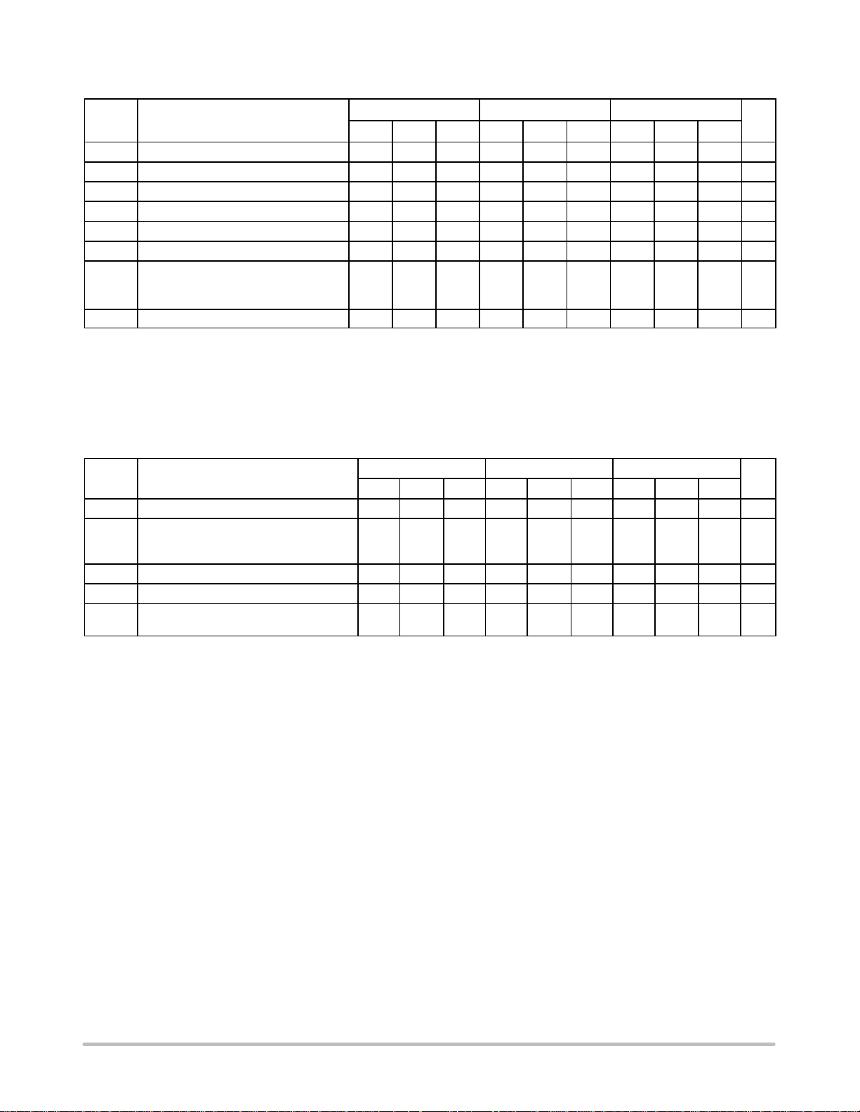
Table 4. 10E SERIES PECL DC CHARACTERISTICS V
= 5.0 V, VEE = 0.0 V (Note 1)
CC
0°C 25°C 85°C
Symbol Characteristic
I
EE
V
OH
V
OL
V
IH
V
IL
I
IH
I
IL
Power Supply Current 32 38 32 38 32 38 mA
Output HIGH Voltage (Note 2) 3980 4070 4160 4020 4105 4190 4090 4185 4280 mV
Output LOW Voltage (Note 2) 3050 3210 3370 3050 3210 3370 3050 3227 3405 mV
Input HIGH Voltage 3830 3995 4160 3870 4030 4190 3940 4110 4280 mV
Input LOW Voltage 3050 3285 3520 3050 3285 3520 3050 3302 3555 mV
Input HIGH Current
Input LOW Current 0.5 0.3 0.5 0.25 0.3 0.2
Min Typ Max Min Typ Max Min Typ Max
D
SEL
200
150
200
150
200
150
Unit
mA
mA
mA
NOTE: Device will meet the specifications after thermal equilibrium has been established when mounted in a test socket or printed circuit
board with maintained transverse airflow greater than 500 lfpm. Electrical parameters are guaranteed only over the declared
operating temperature range. Functional operation of the device exceeding these conditions is not implied. Device specification limit
values are applied individually under normal operating conditions and not valid simultaneously.
1. Input and output parameters vary 1:1 with VCC. VEE can vary −0.46 V / +0.06 V.
2. Outputs are terminated through a 50 W resistor to VCC − 2.0 V.
http://onsemi.com
3
MC10E157, MC100E157
Table 5. 10E SERIES PECL DC CHARACTERISTICS V
= 5.0 V, VEE = 0.0 V (Note 3)
CC
0°C 25°C 85°C
Symbol Characteristic
I
EE
V
OH
V
OL
V
IH
V
IL
I
IH
I
IL
Power Supply Current 32 38 32 38 32 38 mA
Output HIGH Voltage (Note 4) −1020 −930 −840 −980 −895 −810 −910 −815 −720 mV
Output LOW Voltage (Note 4) −1950 −1790 −1630 −1950 −1790 −1630 −1950 −1773 −1595 mV
Input HIGH Voltage −1170 −1005 −840 −1130 −970 −810 −1060 −890 −720 mV
Input LOW Voltage −1950 −1715 −1480 −1950 −1715 −1480 −1950 −1698 −1445 mV
Input HIGH Current
Input LOW Current 0.5 0.3 0.5 0.065 0.3 0.2
Min Typ Max Min Typ Max Min Typ Max
D
SEL
200
150
200
150
200
150
Unit
mA
mA
mA
NOTE: Device will meet the specifications after thermal equilibrium has been established when mounted in a test socket or printed circuit
board with maintained transverse airflow greater than 500 lfpm. Electrical parameters are guaranteed only over the declared
operating temperature range. Functional operation of the device exceeding these conditions is not implied. Device specification limit
values are applied individually under normal operating conditions and not valid simultaneously.
3. Input and output parameters vary 1:1 with VCC. VEE can vary −0.46 V / +0.06 V.
4. Outputs are terminated through a 50 W resistor to VCC − 2.0 V.
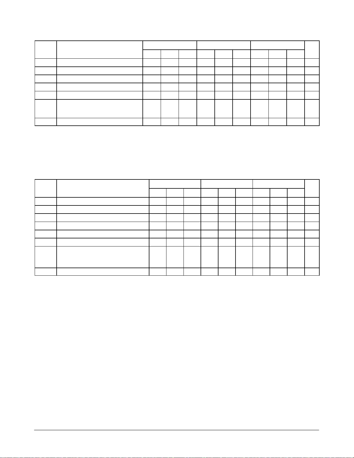
Table 6. 100E SERIES PECL DC CHARACTERISTICS V
= 5.0 V; VEE = 0.0 V (Note 5)
CCx
0°C 25°C 85°C
Symbol Characteristic
I
EE
V
OH
V
OL
V
IH
V
IL
V
BB
I
IH
I
IL
Power Supply Current 32 38 32 38 37 44 mA
Output HIGH Voltage (Note 6) 3975 4050 4120 3975 4050 4120 3975 4050 4120 mV
Output LOW Voltage (Note 6) 3190 3295 3380 3190 3255 3380 3190 3260 3380 mV
Input HIGH Voltage 3835 3975 4120 3835 3975 4120 3835 3975 4120 mV
Input LOW Voltage 3190 3355 3525 3190 3355 3525 3190 3355 3525 mV
Output Voltage Reference 3.62 3.74 3.62 3.74 3.62 3.74 V
Input HIGH Current
Input LOW Current 0.5 0.3 0.5 0.25 0.5 0.2
Min Typ Max Min Typ Max Min Typ Max
D
SEL
200
150
200
150
200
150
Unit
mA
mA
mA
NOTE: Device will meet the specifications after thermal equilibrium has been established when mounted in a test socket or printed circuit
board with maintained transverse airflow greater than 500 lfpm. Electrical parameters are guaranteed only over the declared
operating temperature range. Functional operation of the device exceeding these conditions is not implied. Device specification limit
values are applied individually under normal operating conditions and not valid simultaneously.
5. Input and output parameters vary 1:1 with VCC. VEE can vary −0.46 V / +0.8 V.
6. Outputs are terminated through a 50 W resistor to VCC − 2.0 V.
http://onsemi.com
4
MC10E157, MC100E157
Table 7. 100E SERIES NECL DC CHARACTERISTICS V
= 0 V; VEE = −5.0 V (Note 7)
CCx
0°C 25°C 85°C
Symbol Characteristic
I
EE
V
OH
V
OL
V
IH
V
IL
V
BB
I
IH
I
IL
Power Supply Current 32 38 32 38 37 44 mA
Output HIGH Voltage (Note 8) −1025 −950 −880 −1025 −950 −880 −1025 −950 −880 mV
Output LOW Voltage (Note 8) −1810 −1705 −1620 −1810 −1745 −1620 −1810 −1740 −1620 mV
Input HIGH Voltage −1165 −1025 −880 −1165 −1025 −880 −1165 −1025 −880 mV
Input LOW Voltage −1810 −1645 −1475 −1810 −1645 −1475 −1810 −1645 −1475 mV
Output Voltage Reference −1.38 −1.26 −1.38 −1.26 −1.38 −1.26 V
Input HIGH Current
Input LOW Current 0.5 0.3 0.5 0.25 0.5 0.2
Min Typ Max Min Typ Max Min Typ Max
D
SEL
200
150
200
150
200
150
Unit
mA
mA
mA
NOTE: Device will meet the specifications after thermal equilibrium has been established when mounted in a test socket or printed circuit
board with maintained transverse airflow greater than 500 lfpm. Electrical parameters are guaranteed only over the declared
operating temperature range. Functional operation of the device exceeding these conditions is not implied. Device specification limit
values are applied individually under normal operating conditions and not valid simultaneously.
7. Input and output parameters vary 1:1 with VCC. VEE can vary −0.46 V / +0.8 V.
8. Outputs are terminated through a 50 W resistor to VCC − 2.0 V.
Table 8. AC CHARACTERISTICS V
= 5.0 V; VEE = 0.0 V or V
CCx
= 0.0 V; VEE = −5.0 V (Note 9)
CCx
0°C 25°C 85°C
Symbol Characteristic
f
MAX
t
PLH
t
PHL
t
SKEW
t
JITTER
t
r
t
f
Maximum Toggle Frequency 700 1100 700 1100 700 1100 MHz
Propagation Delay to Output
Within-Device Skew (Note 10) 70 70 70 ps
Random Clock Jitter (RMS) < 1 < 1 < 1 ps
Rise/Fall Time
(20 - 80%) 275 400 650 275 400 650 275 400 650
Min Typ Max Min Typ Max Min Typ Max
D
SEL
220
425
380
600
550
800
220
425
380
600
550
800
220
425
380
600
Unit
ps
550
800
ps
NOTE: Device will meet the specifications after thermal equilibrium has been established when mounted in a test socket or printed circuit
board with maintained transverse airflow greater than 500 lfpm. Electrical parameters are guaranteed only over the declared
operating temperature range. Functional operation of the device exceeding these conditions is not implied. Device specification limit
values are applied individually under normal operating conditions and not valid simultaneously.
9. 10 Series: VEE can vary −0.46 V / +0.06 V.
100 Series: VEE can vary −0.46 V / +0.8 V.
10.Within-device skew is defined as identical transitions on similar paths through a device.
http://onsemi.com
5
MC10E157, MC100E157
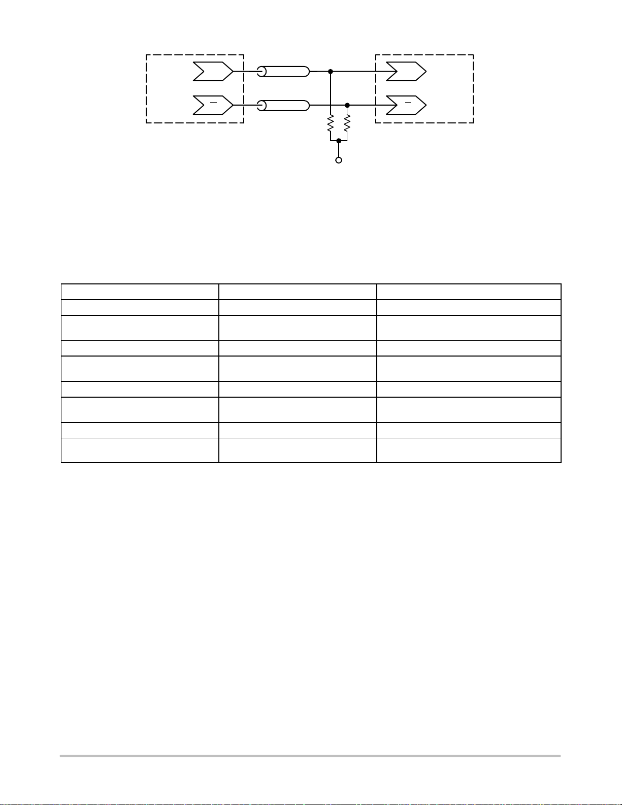
Zo = 50 W
Zo = 50 W
50 W 50 W
V
VTT = VCC − 2.0 V
TT
Receiver
Device
Driver
Device
QD
Q D
Figure 3. Typical Termination for Output Driver and Device Evaluation
(See Application Note AND8020/D − Termination of ECL Logic Devices.)
ORDERING INFORMATION
Device Package Shipping
MC10E157FN PLCC−28 37 Units / Rail
MC10E157FNG PLCC−28
(Pb−Free)
MC10E157FNR2 PLCC−28 500 / Tape & Reel
MC10E157FNR2G PLCC−28
(Pb−Free)
MC100E157FN PLCC−28 37 Units / Rail
MC100E157FNG PLCC−28
(Pb−Free)
MC100E157FNR2 PLCC−28 500 / Tape & Reel
MC100E157FNR2G PLCC−28
(Pb−Free)
†For information on tape and reel specifications, including part orientation and tape sizes, please refer to our Tape and Reel Packaging
Specifications Brochure, BRD8011/D.
37 Units / Rail
500 / Tape & Reel
37 Units / Rail
500 / Tape & Reel
†
Resource Reference of Application Notes
AN1405/D − ECL Clock Distribution Techniques
AN1406/D − Designing with PECL (ECL at +5.0 V)
AN1503/D −
AN1504/D − Metastability and the ECLinPS Family
AN1568/D − Interfacing Between LVDS and ECL
AN1672/D − The ECL Translator Guide
AND8001/D − Odd Number Counters Design
AND8002/D − Marking and Date Codes
AND8020/D − Termination of ECL Logic Devices
AND8066/D − Interfacing with ECLinPS
AND8090/D − AC Characteristics of ECL Devices
ECLinPSt I/O SPiCE Modeling Kit
http://onsemi.com
6
MC10E157, MC100E157
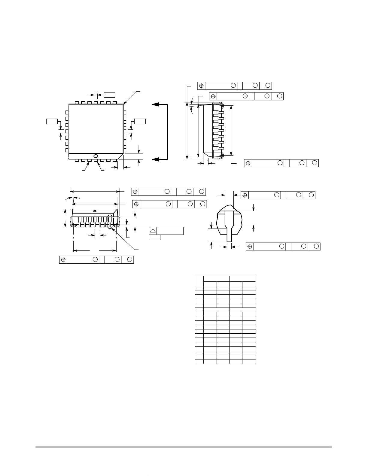
PACKAGE DIMENSIONS
PLCC−28
FN SUFFIX
PLASTIC PLCC PACKAGE
CASE 776−02
ISSUE E
−L−
−N−
28 1
Z
C
G
G1
S
0.010 (0.250) N
L−M
T
S
L−M
T
M
S
S
L−M
T
S
Y BRK
0.007 (0.180) N
B
0.007 (0.180) N
U
M
D
Z
−M−
W
D
V
0.010 (0.250) N
G1X
S
S
L−M
T
S
VIEW D−D
A
0.007 (0.180) N
0.007 (0.180) N
R
E
M
M
S
L−M
T
L−M
T
S
S
S
H
0.007 (0.180) N
M
S
L−M
T
S
K1
0.004 (0.100)
SEATING
J
−T−
PLANE
VIEW S
S
S
K
VIEW S
0.007 (0.180) N
F
M
S
L−M
T
S
NOTES:
1. DATUMS −L−, −M−, AND −N− DETERMINED
WHERE TOP OF LEAD SHOULDER EXITS
PLASTIC BODY AT MOLD PARTING LINE.
2. DIMENSION G1, TRUE POSITION TO BE
MEASURED AT DATUM −T−, SEATING PLANE.
3. DIMENSIONS R AND U DO NOT INCLUDE
MOLD FLASH. ALLOWABLE MOLD FLASH IS
0.010 (0.250) PER SIDE.
4. DIMENSIONING AND TOLERANCING PER
ANSI Y14.5M, 1982.
5. CONTROLLING DIMENSION: INCH.
6. THE PACKAGE TOP MAY BE SMALLER THAN
THE PACKAGE BOTTOM BY UP TO 0.012
(0.300). DIMENSIONS R AND U ARE
DETERMINED AT THE OUTERMOST
EXTREMES OF THE PLASTIC BODY
EXCLUSIVE OF MOLD FLASH, TIE BAR
BURRS, GATE BURRS AND INTERLEAD
FLASH, BUT INCLUDING ANY MISMATCH
BETWEEN THE TOP AND BOTTOM OF THE
PLASTIC BODY.
7. DIMENSION H DOES NOT INCLUDE DAMBAR
PROTRUSION OR INTRUSION. THE DAMBAR
PROTRUSION(S) SHALL NOT CAUSE THE H
DIMENSION TO BE GREATER THAN 0.037
(0.940). THE DAMBAR INTRUSION(S) SHALL
NOT CAUSE THE H DIMENSION TO BE
SMALLER THAN 0.025 (0.635).
DIM MIN MAX MIN MAX
A 0.485 0.495 12.32 12.57
B 0.485 0.495 12.32 12.57
C 0.165 0.180 4.20 4.57
E 0.090 0.110 2.29 2.79
F 0.013 0.019 0.33 0.48
G 0.050 BSC 1.27 BSC
H 0.026 0.032 0.66 0.81
J 0.020 −−− 0.51 −−−
K 0.025 −−− 0.64 −−−
R 0.450 0.456 11.43 11.58
U 0.450 0.456 11.43 11.58
V 0.042 0.048 1.07 1.21
W 0.042 0.048 1.07 1.21
X 0.042 0.056 1.07 1.42
Y −−− 0.020 −−− 0.50
Z 2 10 2 10
__ __
G1 0.410 0.430 10.42 10.92
K1 0.040 −−− 1.02 −−−
MILLIMETERSINCHES
http://onsemi.com
7

MC10E157, MC100E157
ECLinPS is a trademark of Semiconductor Components Industries, LLC (SCILLC).
ON Semiconductor and are registered trademarks of Semiconductor Components Industries, LLC (SCILLC). SCILLC reserves the right to make changes without further notice
to any products herein. SCILLC makes no warranty, representation or guarantee regarding the suitability of its products for any particular purpose, nor does SCILLC assume any liability
arising out of the application or use of any product or circuit, and specifically disclaims any and all liability, including without limitation special, consequential or incidental damages.
“Typical” parameters which may be provided in SCILLC data sheets and/or specifications can and do vary in different applications and actual performance may vary over time. All
operating parameters, including “Typicals” must be validated for each customer application by customer’s technical experts. SCILLC does not convey any license under its patent rights
nor the rights of others. SCILLC products are not designed, intended, or authorized for use as components in systems intended for surgical implant into the body, or other applications
intended to support or sustain life, or for any other application in which the failure of the SCILLC product could create a situation where personal injury or death may occur. Should
Buyer purchase or use SCILLC products for any such unintended or unauthorized application, Buyer shall indemnify and hold SCILLC and its officers, employees, subsidiaries, affiliates,
and distributors harmless against all claims, costs, damages, and expenses, and reasonable attorney fees arising out of, directly or indirectly, any claim of personal injury or death
associated with such unintended or unauthorized use, even if such claim alleges that SCILLC was negligent regarding the design or manufacture of the part. SCILLC is an Equal
Opportunity/Affirmative Action Employer. This literature is subject to all applicable copyright laws and is not for resale in any manner.
PUBLICATION ORDERING INFORMATION
LITERATURE FULFILLMENT:
Literature Distribution Center for ON Semiconductor
P.O. Box 5163, Denver, Colorado 80217 USA
Phone: 303−675−2175 or 800−344−3860 Toll Free USA/Canada
Fax: 303−675−2176 or 800−344−3867 Toll Free USA/Canada
Email: orderlit@onsemi.com
N. American Technical Support: 800−282−9855 Toll Free
USA/Canada
Europe, Middle East and Africa Technical Support:
Phone: 421 33 790 2910
Japan Customer Focus Center
Phone: 81−3−5773−3850
http://onsemi.com
ON Semiconductor Website: www.onsemi.com
Order Literature: http://www.onsemi.com/orderlit
For additional information, please contact your local
Sales Representative
MC10E157/D
8
 Loading...