

查询MC100E210供应商查询MC100E210供应商
MC100LVE210, MC100E210
Low Voltage Dual 1:4, 1:5
Differential Fanout Buffer
ECL/PECL Compatible
The MC100LVE210 is a low voltage, low skew dual differential
ECL fanout buffer designed with clock distribution in mind. The
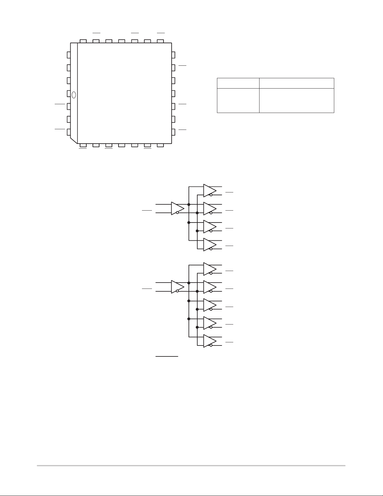
device features two fanout buffers, a 1:4 and a 1:5 buffer, on a single
chip. The device features fully differential clock paths to minimize
both device and system skew. The dual buf fer allows for the fanout of
two signals through a single chip, thus reducing the skew between the
two fundamental signals from a part–to–part skew down to an
output–to–output skew . This capability reduces the skew by a factor of
4 as compared to using two LVE111’s to accomplish the same task.
The MC100LVE210 works from a –3.3V supply while the
MC100E210 provides identical function and performance from a
standard –4.5V 100E voltage supply .
For applications which require a single–ended input, the V
BB
reference voltage is supplied. For single–ended input applications the
VBB reference should be connected to the unused CLK input of a
differential pair and bypassed to ground via a 0.01µf capacitor. The
input signal is then driven into the selected CLK input.
T o ensure that the tight skew specification is met it is necessary that
both sides of the differential output are identically terminated, even if
only one side is being used. In most applications all nine differential
pairs will be used and therefore terminated. In the case where fewer
than nine pairs are used it is necessary to terminate at least the output
pairs adjacent to the output pair being used in order to maintain
minimum skew. Failure to follow this guideline will result in small
degradations of propagation delay (on the order of 10–20ps) of the
outputs being used, while not catastrophic to most designs this will
result in an increase in skew. Note that the package corners isolate
outputs from one another such that the guideline expressed above
holds only for outputs on the same side of the package.
The MC100LVE210, as with most ECL devices, can be operated
from a positive VCC supply in PECL mode. This allows the L VE210 to
be used for high performance clock distribution in +3.3V systems.
Designers can take advantage of the LVE210’s performance to
distribute low skew clocks across the backplane or the board. In a
PECL environment series or Thevenin line terminations are typically
used as they require no additional power supplies, if parallel
termination is desired a terminating voltage of VCC–2.0V will need to
be provided. For more information on using PECL, designers should
refer to Application Note AN1406/D.
• Dual Differential Fanout Buf fers
• 200ps Part–to–Part Skew
• 50ps Typical Output–to–Output Skew
• Low Voltage ECL/PECL Compatible
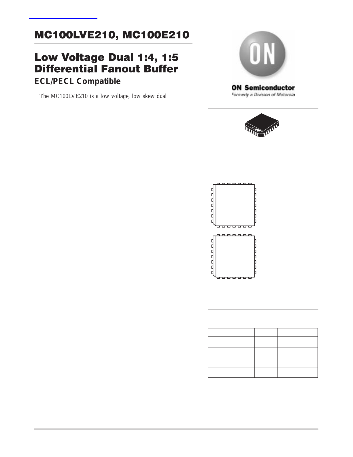
• 28–lead PLCC Packaging
http://onsemi.com
PLCC PACKAGE
FN SUFFIX
CASE 776
MARKING DIAGRAM*
MC100L VE210
AWLYYWW
MC100E210FN
AWLYYWW
*For additional information, see Application Note
AND8002/D
ORDERING INFORMATION
Device Package Shipping
MC100L VE210FN PLCC 37 Units / Rail
MC100L VE210FNR2 PLCC 500 Tape & Reel
MC100E210FN PLCC 37 Units / Rail
MC100E210FNR2 PLCC 500 Tape & Reel
A = Assembly Location
WL = Wafer Lot
YY = Year
WW = Work Week
A = Assembly Location
WL = Wafer Lot
YY = Year
WW = Work Week
Semiconductor Components Industries, LLC, 1999
February , 2000 – Rev. 2
1 Publication Order Number:
MC100L VE210/D
MC100LVE210, MC100E210
V
EE
V
BB
CLKa
V
CC
CLKa
CLKb
CLKb
Qa0 Qa0 Qa1 V
25 24 23 22 21 20 19
26
27
28
1
2
3
4
Pinout: 28–Lead PLCC
(Top View)
567891011
Qb4 Qb3 Qb2Qb4 V
Qa1 Qa2 Qa2
CCO
Qb3 Qb2
CCO
CLKa
CLKa
Qa3
18
Qa3
17
Qb0
16
15
V
CCO
14
Qb0
13
Qb1
12
Qb1
LOGIC SYMBOL
PIN NAMES
Pins
CLKa, CLKb
Qa0:3, Qb0:4
V
BB
Qa0
Qa0
Qa1
Qa1
Qa2
Qa2
Qa3
Qa3
Function
Differential Input Pairs
Differential Outputs
VBB Output
CLKb
CLKb
V
BB
Qb0
Qb0
Qb1
Qb1
Qb2
Qb2
Qb3
Qb3
Qb4
Qb4
http://onsemi.com
2
MC100LVE210, MC100E210
MC100LVE210
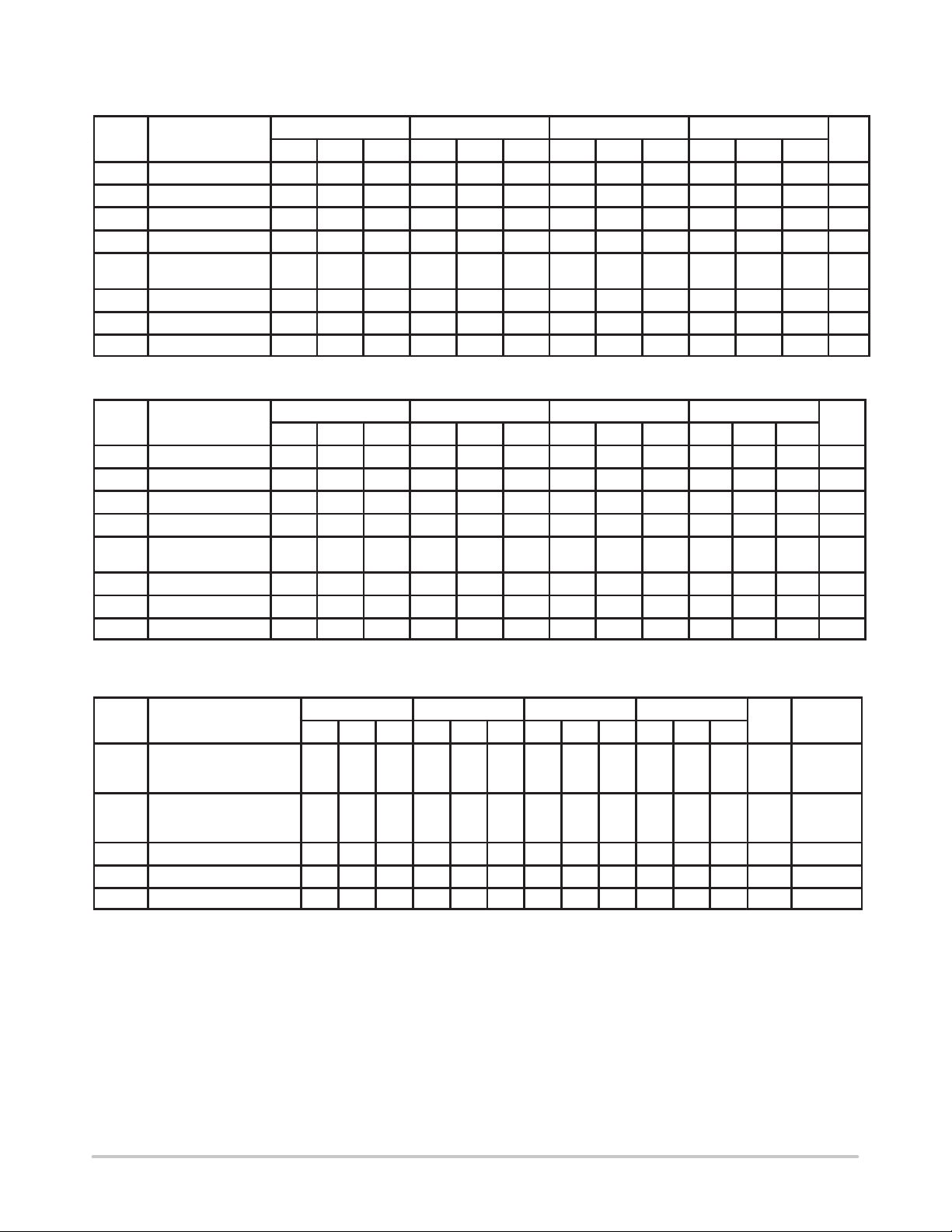
ECL DC CHARACTERISTICS
–40°C 0°C 25°C 85°C
Symbol Characteristic Min Typ Max Min Typ Max Min Typ Max Min Typ Max Unit
V
OH
V
OL
V
IH
V
IL
V
BB
V
EE
I
IH
I
EE
MC100L VE210
PECL DC CHARACTERISTICS
Symbol Characteristic Min Typ Max Min Typ Max Min Typ Max Min Typ Max Unit
V
OH
V
OL
V
IH
V
IL
V
BB
V
CC
I
IH
I
EE
1. These values are for VCC = 3.3V. Level Specifications will vary 1:1 with VCC.
MC100LVE210
AC CHARACTERISTICS (VEE = VEE (min) to VEE (max); VCC = V
Symbol Characteristic Min Typ Max Min Typ Max Min Typ Max Min Typ Max Unit Condition
t
PLH
t
PHL
t
skew
V
PP
V
CMR
tr/t
1. The differential propagation delay is defined as the delay from the crossing points of the dif ferential input signals to the crossing point of the
2. The single-ended propagation delay is defined as the delay from the 50% point of the input signal to the 50% point of the output signal.
3. The within–device skew is defined as the worst case difference between any two similar delay paths within a single device.
4. VPP(min) is defined as the minimum input differential voltage which will cause no increase in the propagation delay . The VPP(min) is AC limited
5. V
Output HIGH Voltage –1.085 –1.005 –0.880 –1.025 –0.955 –0.880 –1.025 –0.955 –0.880 –1.025 –0.955 –0.880 V
Output LOW Voltage –1.830 –1.695 –1.555 –1.810 –1.705 –1.620 –1.810 –1.705 –1.620 –1.810 –1.705 –1.620 V
Input HIGH Voltage –1.165 –0.880 –1.165 –0.880 –1.165 –0.880 –1.165 –0.880 V
Input LOW Voltage –1.810 –1.475 –1.810 –1.475 –1.810 –1.475 –1.810 –1.475 V
Output Reference
Voltage
Power Supply Voltage –3.0 –3.8 –3.0 –3.8 –3.0 –3.8 –3.0 –3.8 V
Input HIGH Current 150 150 150 150 µA
Power Supply Current 55 55 55 65 mA
Output HIGH Voltage12.215 2.295 2.42 2.275 2.345 2.420 2.275 2.345 2.420 2.275 2.345 2.420 V
Output LOW Voltage11.47 1.605 1.745 1.490 1.595 1.680 1.490 1.595 1.680 1.490 1.595 1.680 V
Input HIGH Voltage
Input LOW Voltage
Output Reference
1
Voltage
Power Supply Voltage 3.0 3.8 3.0 3.8 3.0 3.8 3.0 3.8 V
Input HIGH Current 150 150 150 150 µA
Power Supply Current 55 55 55 65 mA
Propagation Delay to Output
IN (differential)
IN (single–ended)
Within–Device SkewQa Qb
Part–to–Part Skew (Diff)
Minimum Input Swing 500 500 500 500 mV Note 4
Common Mode Range –1.5 –0.4 –1.5 –0.4 –1.5 –0.4 –1.5 –0.4 V Note 5
Output Rise/Fall Time 200 600 200 600 200 600 200 600 ps 20%–80%
f
Qa Qa,Qb Qb
–1.38 –1.26 –1.38 –1.26 –1.38 –1.26 –1.38 –1.26 V
–40°C 0°C 25°C 85°C
1
2.135 2.420 2.135 2.420 2.135 2.420 2.135 2.420 V
1
1.490 1.825 1.490 1.825 1.490 1.825 1.490 1.825 V
1.92 2.04 1.92 2.04 1.92 2.04 1.92 2.04 V
= GND)
CCO
–40°C 0°C 25°C 85°C
475
400
675
700
505075
200
475
400
75
675
700
503075
200
500
450
50
700
750
503075
200
500
450
503075
50
ps
700
750
ps Note 3
50
200
differential output signals.
for the LVE210 as a differential input as low as 50 mV will still produce full ECL levels at the output.
is defined as the range within which the VIH level may vary, with the device still meeting the propagation delay specification. The V
CMR
level must be such that the peak to peak voltage is less than 1.0 V and greater than or equal to VPP(min).
Note 1
Note 2
IL
http://onsemi.com
3

MC100LVE210, MC100E210
MC100E210
ECL DC CHARACTERISTICS
–40°C 0°C 25°C 85°C
Symbol Characteristic Min Typ Max Min Typ Max Min Typ Max Min Typ Max Unit
V
OH
V
OL
V
IH
V
IL
V
BB
V
EE
I
IH
I
EE
MC100E210
PECL DC CHARACTERISTICS
Symbol Characteristic Min Typ Max Min Typ Max Min Typ Max Min Typ Max Unit
V
OH
V
OL
V
IH
V
IL
V
BB
V
CC
I
IH
I
EE
1. These values are for VCC = 5.0V. Level Specifications will vary 1:1 with VCC.
MC100E210
AC CHARACTERISTICS (VEE = VEE (min) to VEE (max); VCC = V
Symbol Characteristic Min Typ Max Min Typ Max Min Typ Max Min Typ Max Unit Condition
t
PLH
t
PHL
t
skew
V
PP
V
CMR
tr/t
1. The differential propagation delay is defined as the delay from the crossing points of the dif ferential input signals to the crossing point of the
2. The single-ended propagation delay is defined as the delay from the 50% point of the input signal to the 50% point of the output signal.
3. The within–device skew is defined as the worst case difference between any two similar delay paths within a single device.
4. VPP(min) is defined as the minimum input differential voltage which will cause no increase in the propagation delay . The VPP(min) is AC limited
5. V
Output HIGH Voltage –1.085 –1.005 –0.880 –1.025 –0.955 –0.880 –1.025 –0.955 –0.880 –1.025 –0.955 –0.880 V
Output LOW Voltage –1.830 –1.695 –1.555 –1.810 –1.705 –1.620 –1.810 –1.705 –1.620 –1.810 –1.705 –1.620 V
Input HIGH Voltage –1.165 –0.880 –1.165 –0.880 –1.165 –0.880 –1.165 –0.880 V
Input LOW Voltage –1.810 –1.475 –1.810 –1.475 –1.810 –1.475 –1.810 –1.475 V
Output Reference
Voltage
Power Supply Voltage –5.25 –4.2 –5.25 –4.2 –5.25 –4.2 –5.25 –4.2 V
Input HIGH Current 150 150 150 150 µA
Power Supply Current 55 55 55 65 mA
Output HIGH Voltage13.915 3.995 4.12 3.975 4.045 4.12 3.975 4.045 4.12 3.975 4.045 4.12 V
Output LOW Voltage13.170 3.305 3.445 3.19 3.295 3.38 3.19 3.295 3.38 3.19 3.295 3.38 V
Input HIGH Voltage
Input LOW Voltage
Output Reference
1
Voltage
Power Supply Voltage 4.75 5.25 4.75 5.25 4.75 5.25 4.75 5.25 V
Input HIGH Current 150 150 150 150 µA
Power Supply Current 55 55 55 65 mA
Propagation Delay to Output
IN (differential)
IN (single–ended)
Within–Device SkewQa Qb
Part–to–Part Skew (Diff)
Minimum Input Swing 500 500 500 500 mV Note 4
Common Mode Range –1.5 –0.4 –1.5 –0.4 –1.5 –0.4 –1.5 –0.4 V Note 5
Output Rise/Fall Time 200 600 200 600 200 600 200 600 ps 20%–80%
f
Qa Qa,Qb Qb
–1.38 –1.26 –1.38 –1.26 –1.38 –1.26 –1.38 –1.26 V
–40°C 0°C 25°C 85°C
1
3.835 4.12 3.835 4.12 3.835 4.12 3.835 4.12 V
1
3.190 3.525 3.190 3.525 3.190 3.525 3.190 3.525 V
3.62 3.74 3.62 3.74 3.62 3.74 3.62 3.74 V
= GND)
CCO
–40°C 0°C 25°C 85°C
475
400
675
700
505075
200
475
400
75
675
700
503075
200
500
450
50
700
750
503075
200
500
450
503075
50
ps
700
750
ps Note 3
50
200
differential output signals.
for the E210 as a differential input as low as 50 mV will still produce full ECL levels at the output.
is defined as the range within which the VIH level may vary, with the device still meeting the propagation delay specification. The V
CMR
level must be such that the peak to peak voltage is less than 1.0 V and greater than or equal to VPP(min).
Note 1
Note 2
IL
http://onsemi.com
4

MC100LVE210, MC100E210
P ACKAGE DIMENSIONS
PLCC PACKAGE
FN SUFFIX
CASE 776–02
ISSUE D
-L-
C
0.010 (0.250)
28 1
Z
G
G1
TL
-N-
–M
Y BRK
0.007 (0.180)
B
0.007 (0.180)
U
TL
–M
TL
SNSM
SNSM
–M
D
Z
-M-
D
W
V
X
G1
0.010 (0.250)
TL
–M
SNSS
VIEW D-D
0.007 (0.180)
A
0.007 (0.180)
R
E
0.004 (0.100)
SEATING
-T-
J
PLANE
VIEW S
SNSS
TL
TL
–M
–M
SNSM
SNSM
0.007 (0.180)
H
TL
–M
SNSM
K1
K
0.007 (0.180)
F
TL
–M
SNSM
VIEW S
NOTES:
1. DATUMS -L-, -M-, AND -N- DETERMINED
WHERE TOP OF LEAD SHOULDER EXITS
PLASTIC BODY AT MOLD PARTING LINE.
2. DIM G1, TRUE POSITION TO BE MEASURED
AT DATUM -T-, SEATING PLANE.
3. DIM R AND U DO NOT INCLUDE MOLD FLASH.
ALLOWABLE MOLD FLASH IS 0.010 (0.250)
PER SIDE.
4. DIMENSIONING AND TOLERANCING PER ANSI
Y14.5M, 1982.
5. CONTROLLING DIMENSION: INCH.
6. THE PACKAGE TOP MAY BE SMALLER THAN
THE PACKAGE BOTTOM BY UP TO 0.012
(0.300). DIMENSIONS R AND U ARE
DETERMINED AT THE OUTERMOST
EXTREMES OF THE PLASTIC BODY
EXCLUSIVE OF MOLD FLASH, TIE BAR
BURRS, GATE BURRS AND INTERLEAD
FLASH, BUT INCLUDING ANY MISMATCH
BETWEEN THE TOP AND BOTTOM OF THE
PLASTIC BODY.
7. DIMENSION H DOES NOT INCLUDE DAMBAR
PROTRUSION OR INTRUSION. THE DAMBAR
PROTRUSION(S) SHALL NOT CAUSE THE H
DIMENSION TO BE GREATER THAN 0.037
(0.940). THE DAMBAR INTRUSION(S) SHALL
NOT CAUSE THE H DIMENSION TO BE
SMALLER THAN 0.025 (0.635).
http://onsemi.com
INCHES MILLIMETERS
MIN MINMAX MAX
DIM
0.485
0.485
0.165
0.090
0.013
0.050 BSC
0.026
0.020
0.025
0.450
0.450
0.042
0.042
0.042
—
2°
0.410
0.040
0.495
0.495
0.180
0.110
0.019
0.032
0.456
0.456
0.048
0.048
0.056
0.020
10°
0.430
—
—
—
A
B
C
E
F
G
H
J
K
R
U
V
W
X
Y
Z
G1
K1
12.32
12.32
4.20
2.29
0.33
0.66
0.51
0.64
11.43
11.43
1.07
1.07
1.07
10.42
1.02
—
2°
1.27 BSC
12.57
12.57
4.57
2.79
0.48
0.81
11.58
11.58
1.21
1.21
1.42
0.50
10°
10.92
—
—
—
5

Notes
MC100LVE210, MC100E210
http://onsemi.com
6

Notes
MC100LVE210, MC100E210
http://onsemi.com
7

MC100LVE210, MC100E210
ON Semiconductor and are trademarks of Semiconductor Components Industries, LLC (SCILLC). SCILLC reserves the right to make changes
without further notice to any products herein. SCILLC makes no warranty , representation or guarantee regarding the suitability of its products for any particular
purpose, nor does SCILLC assume any liability arising out of the application or use of any product or circuit, and specifically disclaims any and all liability ,
including without limitation special, consequential or incidental damages. “Typical” parameters which may be provided in SCILLC data sheets and/or
specifications can and do vary in different applications and actual performance may vary over time. All operating parameters, including “Typicals” must be
validated for each customer application by customer’s technical experts. SCILLC does not convey any license under its patent rights nor the rights of others.
SCILLC products are not designed, intended, or authorized for use as components in systems intended for surgical implant into the body, or other applications
intended to support or sustain life, or for any other application in which the failure of the SCILLC product could create a situation where personal injury or
death may occur. Should Buyer purchase or use SCILLC products for any such unintended or unauthorized application, Buyer shall indemnify and hold
SCILLC and its officers, employees, subsidiaries, affiliates, and distributors harmless against all claims, costs, damages, and expenses, and reasonable
attorney fees arising out of, directly or indirectly , any claim of personal injury or death associated with such unintended or unauthorized use, even if such claim
alleges that SCILLC was negligent regarding the design or manufacture of the part. SCILLC is an Equal Opportunity/Affirmative Action Employer .
PUBLICATION ORDERING INFORMATION
NORTH AMERICA Literature Fulfillment:
Literature Distribution Center for ON Semiconductor
P.O. Box 5163, Denver, Colorado 80217 USA
Phone: 303–675–2175 or 800–344–3860 Toll Free USA/Canada
Fax: 303–675–2176 or 800–344–3867 Toll Free USA/Canada
Email: ONlit@hibbertco.com
Fax Response Line: 303–675–2167 or 800–344–3810 T oll Free USA/Canada
N. American Technical Support: 800–282–9855 Toll Free USA/Canada
EUROPE: LDC for ON Semiconductor – European Support
German Phone: (+1) 303–308–7140 (M–F 1:00pm to 5:00pm Munich Time)
Email: ONlit–german@hibbertco.com
French Phone: (+1) 303–308–7141 (M–F 1:00pm to 5:00pm Toulouse Time)
Email: ONlit–french@hibbertco.com
English Phone: (+1) 303–308–7142 (M–F 12:00pm to 5:00pm UK Time)
Email: ONlit@hibbertco.com
EUROPEAN TOLL–FREE ACCESS*: 00–800–4422–3781
*Available from Germany, France, Italy, England, Ireland
CENTRAL/SOUTH AMERICA:
Spanish Phone: 303–308–7143 (Mon–Fri 8:00am to 5:00pm MST)
Email: ONlit–spanish@hibbertco.com
ASIA/PACIFIC : LDC for ON Semiconductor – Asia Support
Phone: 303–675–2121 (Tue–Fri 9:00am to 1:00pm, Hong Kong Time)
T oll Free from Hong Kong & Singapore:
001–800–4422–3781
Email: ONlit–asia@hibbertco.com
JAPAN: ON Semiconductor, Japan Customer Focus Center
4–32–1 Nishi–Gotanda, Shinagawa–ku, T okyo, Japan 141–8549
Phone: 81–3–5740–2745
Email: r14525@onsemi.com
ON Semiconductor Website: http://onsemi.com
For additional information, please contact your local
Sales Representative.
http://onsemi.com
8
MC100L VE210/D
 Loading...