

Page 1
查询CS3844供应商
CS5253B−1
3.0 A LDO 5−Pin Adjustable
Linear Regulator with
Remote Sense Applications
This new very low dropout linear regulator reduces total power
dissipation in the application. To achieve very low dropout, the
internal pass transistor is powered separately from the control
circuitry. Furthermore, with the control and power inputs tied together,
this device can be used in single supply configuration and still offer a
better dropout voltage than conventional PNP − NPN based LDO
regulators. In this mode the dropout is determined by the minimum
control voltage.
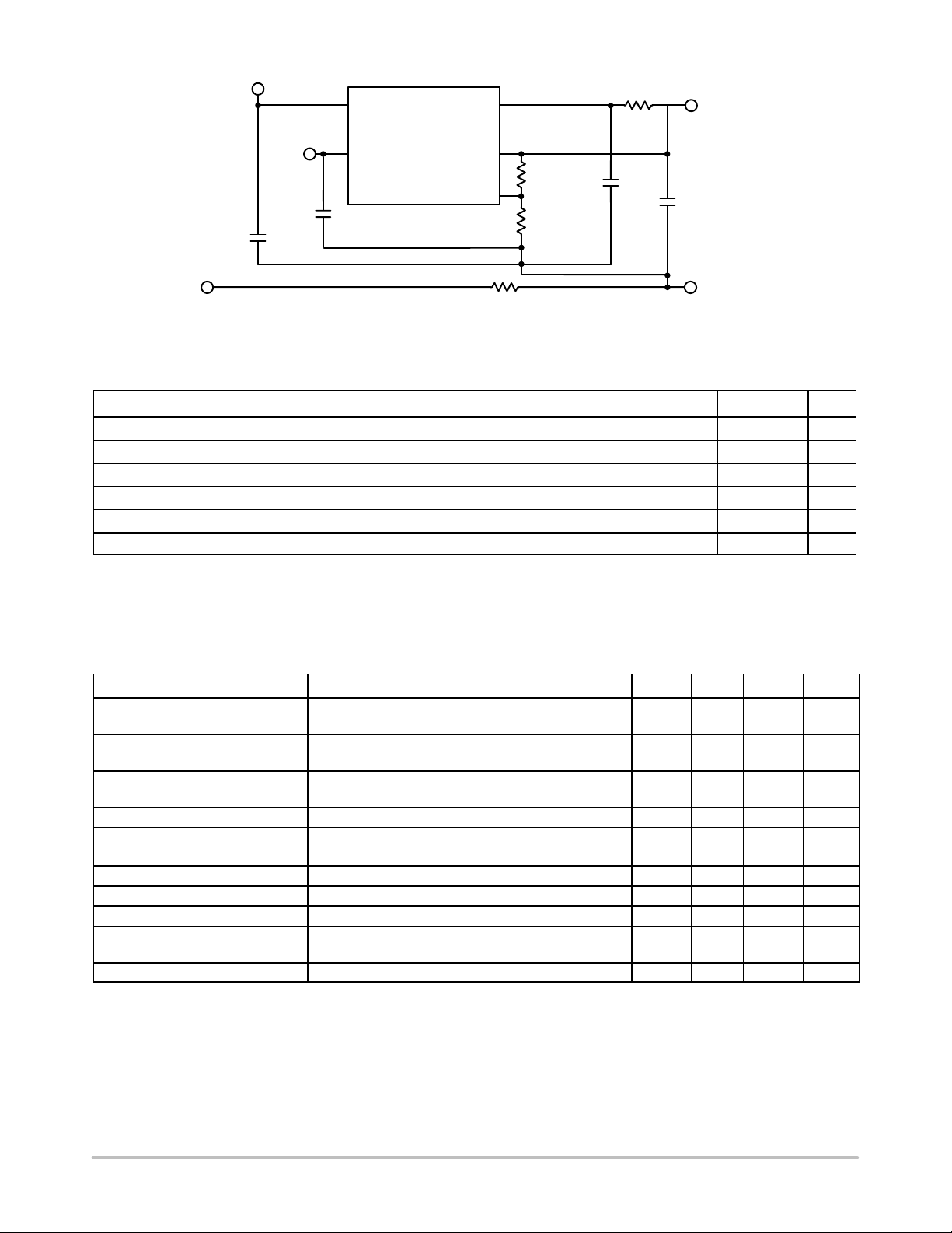
The CS5253B−1 is offered in a five−terminal D
which allows for the implementation of a remote−sense pin permitting
very accurate regulation of output voltage directly at the load, where it
counts, rather than at the regulator. This remote sensing feature
virtually eliminates output voltage variations due to load changes and
resistive voltage drops. Typical load regulation measured at the sense
pin is less than 1.0 mV for an output voltage of 2.5 V with a load step
of 10 mA to 3.0 A.
The CS5253B−1 has a very fast transient loop response which can
be adjusted using a small capacitor on the Adjust pin.
Internal protection circuitry provides for “bust−proof” operation,
similar to three−terminal regulators. This circuitry, which includes
overcurrent, short circuit, and overtemperature protection will
self protect the regulator under all fault conditions.
The CS5253B−1 is ideal for generating a 2.5 V supply to power
graphics controllers used on VGA cards. Its remote sense and low
value capacitance requirements make this a low cost, high
performance solution. The CS5253B−1 is optimized from the
CS5253−1 to allow a lower value of output capacitor to be used at the
expense of a slower transient response.
2
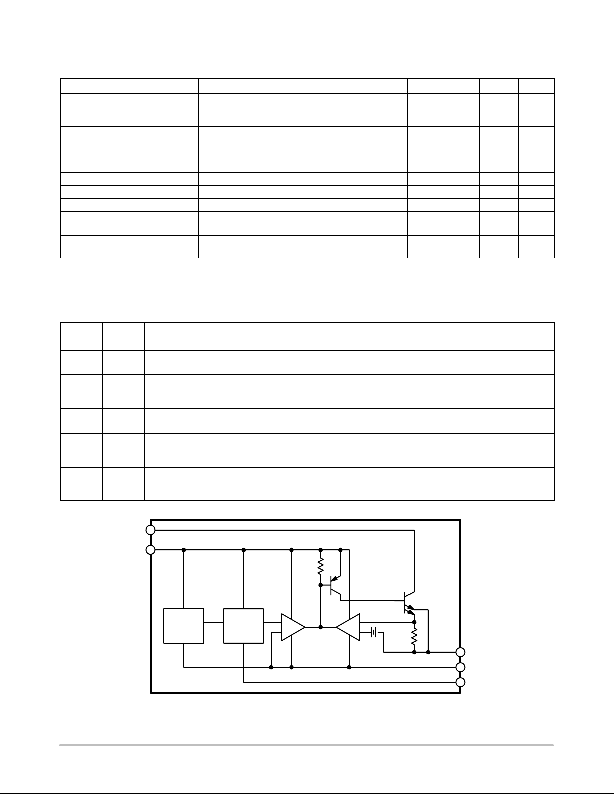
PAK−5 package,
http://onsemi.com
1
5
D2PAK−5
DP SUFFIX
CASE 936AC
MARKING DIAGRAM
5253B−1
AWLYWW
1
A = Assembly Location
WL = Wafer Lot
Y = Year
WW = Work Week
Tab = V
Pin 1. V
2. Adjust
3. V
4. V
5. V
CS
OUT
SENSE
OUT
CONTROL
POWER
Features
• Pb−Free Package is Available*
• V
• V
• V
Range is 1.25 V to 5.0 V @ 3.0 A
OUT
Dropout < 0.40 V @ 3.0 A
POWER
CONTROL
Dropout < 1.05 V @ 3.0 A
• 1.0% Trimmed Reference
• Fast Transient Response
• Remote Voltage Sensing
• Thermal Shutdown
• Current Limit
• Short Circuit Protection
• Drop−In Replacement for EZ1582
• Backwards Compatible with 3−Pin Regulators
• Very Low Dropout Reduces Total Power Consumption
*For additional information on our Pb−Free strategy and soldering details, please
download the ON Semiconductor Soldering and Mounting Techniques
Reference Manual, SOLDERRM/D.
Semiconductor Components Industries, LLC, 2004
June, 2004 − Rev. 5
1 Publication Order Number:
ORDERING INFORMATION
Device Package Shipping
CS5253B−1GDP5 D2P AK−5 50 Units/Rail
CS5253B−1GDPR5 D
CS5253B−1GDPR5G D2PAK−5
†For information on tape and reel specifications,
including part orientation and tape sizes, please
refer to our Tape and Reel Packaging Specifications
Brochure, BRD8011/D.
2
P AK−5 750 Tape & Reel
(Pb−Free)
750 Tape & Reel
CS5253B−1/D
†
Page 2
CS5253B−1
5.0 V
V
CONTROL
V
OUT
R
DIS
2.5 V @ 3.0 A
CS5253B−1
GND
3.3 V
10 F
10 V
V
POWER
100 F
5.0 V
V
SENSE
Adjust
33 F
124
5.0 V
124
C
LOAD
(Optional)
GND
R
DIS
Figure 1. Application Diagram
MAXIMUM RATINGS
Rating Value Unit
V
Input Voltage 6.0 V
POWER
V
CONTROL
Operating Junction Temperature Range, T
Storage Temperature Range −65 to +150 °C
ESD Damage Threshold 2.0 kV
Lead Temperature Soldering: Reflow: (SMD styles only) (Note 1) 230 peak °C
Maximum ratings are those values beyond which device damage can occur. Maximum ratings applied to the device are individual stress limit
values (not normal operating conditions) and are not valid simultaneously . If these limits are exceeded, device functional operation is not implied,
damage may occur and reliability may be affected.
1. 60 second maximum above 183°C.
Input Voltage 13 V
J
0 to 150 °C
ELECTRICAL CHARACTERISTICS (0°C ≤ T
≤ 70°C; 0°C ≤ TJ ≤ 150°C; V
A
SENSE
= V
OUT
and V
= 0 V; unless
ADJ
otherwise specified)
Characteristic Test Conditions Min Typ Max Unit
Reference Voltage V
Line Regulation V
Load Regulation V
Minimum Load Current (Note 2) V
Control Pin Current (Note 3) V
Adjust Pin Current V
Current Limit V
Short Circuit Current V
Ripple Rejection (Note 4) V
CONTROL
CONTROL
CONTROL
CONTROL
CONTROL
V
CONTROL
CONTROL
CONTROL
CONTROL
CONTROL
= 2.75 V to 12 V, V
I
= 10 mA to 3.0 A
OUT
= 2.5 V to 12 V, V
I
= 10 mA
OUT
= 2.75 V, V
I
= 10 mA to 3.0 A, with Remote Sense
OUT
= 5.0 V, V
POWER
= 2.75 V, V
= 2.75 V, V
= 2.75 V, V
= 2.75 V, V
= 2.75 V, V
= V
120 Hz, I
POWER
= 3.0 A, C
OUT
POWER
POWER
= 2.05 V,
POWER
= 3.3 V, V
= 2.05 V, I
POWER
= 2.05 V, I
POWER
= 2.05 V, I
POWER
= 2.05 V, V
POWER
= 2.05 V, V
POWER
= 3.25 V, V
= 0.1 F
ADJ
RIPPLE
= 2.05 V to 5.5 V,
1.237
1.250 1.263
(−1.0%)
= 1.75 V to 5.5 V,
− 0.02 0.2 %
− 0.04 0.3 %
= +1.0% − 5.0 10 mA
OUT
= 100 mA
OUT
= 3.0 A
OUT
= 10 mA − 60 120 A
OUT
= −4.0% 3.1 4.0 − A
OUT
= 0 V 2.0 3.5 − A
OUT
= 1.0 V
P−P
@
−
−
6.0
35
60 80 − dB
(+1.0%)
10
120
V
mA
mA
Thermal Regulation 30 ms Pulse, TA = 25°C − 0.002 − %/W
2. The minimum load current is the minimum current required to maintain regulation. Normally the current in the resistor divider used to set the
output voltage is selected to meet the minimum load current requirement.
3. The V
CONTROL
ratio. The minimum value is equal to the quiescent current of the device.
pin current is the drive current required for the output transistor. This current will track output current with roughly a 1:100
4. This parameter is guaranteed by design and is not 100% production tested.
http://onsemi.com
2
Page 3
CS5253B−1
ELECTRICAL CHARACTERISTICS (continued) (0°C ≤ T
≤ 70°C; 0°C ≤ TJ ≤ 150°C; V
A
SENSE
= V
OUT
and V
= 0 V; unless
ADJ
otherwise specified.)
Characteristic
V
CONTROL
V
POWER
Dropout Voltage
(Minimum V
(Note 5)
Dropout Voltage
(Minimum V
(Note 5)
CONTROL
POWER
− V
− V
OUT
OUT
V
= 2.05 V, I
)
)
POWER
V
POWER
V
POWER
V
CONTROL
V
CONTROL
V
CONTROL
= 2.05 V, I
= 2.05 V, I
RMS Output Noise Freq = 10 Hz to 10 kHz, TA = 25°C − 0.003 − %V
Test Conditions Min Typ Max Unit
= 2.75 V, I
= 2.75 V, I
= 2.75 V, I
= 100 mA
OUT
= 1.0 A
OUT
= 3.0 A
OUT
OUT
OUT
OUT
= 100 mA
= 1.0 A
= 3.0 A
−
−
−
−
−
−
0.90
1.00
1.05
0.05
0.15
0.40
1.15
1.15
1.30
0.15
0.25
0.60
V
V
V
V
V
V
OUT
Temperature Stability − 0.5 − − %
Thermal Shutdown (Note 6) − 150 180 210 °C
Thermal Shutdown Hysteresis − − 25 − °C
V
CONTROL
V
POWER
5. Dropout is defined as either the minimum control voltage (V
Supply Only Output
Current
Supply Only Output
Current
required to maintain 1.0% regulation at a particular load current.
V
CONTROL
V
ADJ
V
POWER
V
ADJ
= 13 V, V
= V
OUT
= 6.0 V, V
= V
OUT
= V
= V
POWER
SENSE
CONTROL
SENSE
CONTROL
Not Connected,
= 0 V
Not Connected,
= 0 V
) or minimum power voltage (V
− − 50 mA
− 0.1 1.0 mA
) to output voltage differential
POWER
6. This parameter is guaranteed by design, but not parametrically tested in production. However, a 100% thermal shutdown functional test
is performed on each part.
PACKAGE PIN DESCRIPTION
Package
Pin #
1 V
2 Adjust This pin is connected to the low side of the internally trimmed 1.0% bandgap reference voltage and carries a bias
3 V
4 V
5 V
Pin
Symbol
SENSE
OUT
CONTRO
L
POWER
Function
This Kelvin sense pin allows for remote sensing of the output voltage at the load for improved regulation. It is
internally connected to the positive input of the voltage sensing error amplifier.
current of about 50 A. A resistor divider from Adjust to V
Also, transient response can be improved by adding a small bypass capacitor from this pin to ground.
and from Adjust to ground sets the output voltage.
OUT
This pin is connected to the emitter of the power pass transistor and provides a regulated voltage capable of
sourcing 3.0 A of current.
This is the supply voltage for the regulator control circuitry. For the device to regulate, this voltage should be between 0.9 V and 1.3 V (depending on the output current) greater than the output voltage. The control pin current
will be about 1.0% of the output current.
This is the power input voltage. This pin is physically connected to the collector of the power pass transistor. For
the device to regulate, this voltage should be between 0.1 V and 0.6 V greater than the output voltage depending
on the output current. The output load current of 3.0 A is supplied through this pin.
V
POWER
V
CONTROL
BIAS
and
TSD
EA IA
V
REF
−
+
Figure 2. Block Diagram
http://onsemi.com
3
+
−
V
OUT
V
SENSE
Adjust
Page 4

CS5253B−1
TYPICAL PERFORMANCE CHARACTERISTICS
1.253
1.252
0.12
0.10
TJ = 120°C
1.251
1.250
0.08
0.06
TJ = 20°C
1.249
Reference Voltage (V)
1.248
1.247
0 20 40 60 80 120
Junction Temperature (°C)
100
0.04
Load Regulation (%)
0.02
0
0 0.5 1.0 1.5 2.0 3.0
Output Current (A)
TJ = 0°C
2.5
Figure 3. Reference Voltage vs Junction Temperature Figure 4. Load Regulation vs Output Current
V
OUT
CS5253−1
= 330 F
C
V
CONTROL
V
POWER
= 2.5 V
V
OUT
C
CONTROL
C
= 0.1 F
ADJ
15 A/s 80 A/s
= 5.0 V
= 3.3 V
= 10 F
OUT
V
OUT
CS5253B−1
= 33 F
C
OUT
I
LOAD
10 mA to 3.0 A
Figure 5. Transient Response Comparison between
5.0
4.5
4.0
3.5
3.0
2.5
2.0
1.5
Output Current (A)
1.0
0.5
Measured at V
0
01 23 4 65
Figure 6. Output Current vs V
OUT
V
POWER
= −1.0%
− V
OUT
(V)
POWER
− V
CS5253−1 and CS5253B−1
OUT
(A)
ADJ
I
85
80
75
70
65
Minimum Load Current (A)
1200
1150
1100
1050
1000
950
900
V
POWER
V
OUT
= 3.3 V
= +1.0%
850
60
0 20 40 60 80 140100
Junction Temperature (°C)
120
800
1.0 2.0 3.0 4.0 6.05.0
V
CONTROL
7.0 8.0 9.0 10 11
− V
OUT
Figure 7. Adjust Pin Current vs Junction Temperature Figure 8. Minimum Load Current vs V
http://onsemi.com
4
(V)
CONTROL
− V
OUT
Page 5

CS5253B−1
5
3.9
3.8
V
CONTROL
V
POWER
= 5.0 V
= 3.3 V
3.7
3.6
3.5
3.4
Short Circuit Output Current Limit (A)
3.3
020 6040 140
80 120100
Junction Temperature (°C)
Figure 9. Short Circuit Output Current vs Junction
Temperature
12
V
CONTROL
10
V
OUT
V
POWER
8
(mA)
6
OUT
I
4
2
0
020 6040 140
= 13 V
= 0 V
Not Connected
80 120100
Junction Temperature (°C)
90
80
70
60
50
VIN − V
40
I
30
20
10
10
1
OUT
V
RIPPLE
C
OUT
C
ADJ
Ripple Rejection (dB)
OUT
= 3.0 A
= 1.0 V
= 22 F
= 0.1 F
2
10
= 2.0 V
P−P
10
3
10
4
Frequency (Hz)
Figure 10. Ripple Rejection vs Frequency
1100
V
1000
Dropout Voltage (mV)
900
CONTROL
V
800
0 0.5 1.0 1.5 2.0 3.0
POWER
= 2.05 V
TJ = 20°C
TJ = 0°C
Output Current (A)
Output Current (A)
TJ = 120°C
10
5
2.5
10
6
Figure 11. V
CONTROL
Only Output Current vs Junction
Temperature
500
450
400
TJ = 120°C
350
300
250
Dropout Voltage (V)
200
150
POWER
V
50
0
0 0.5 1.0 1.5 2.0 3.02.5
Output Current (A)
Figure 13. V
Dropout Voltage vs Output
POWER
Current
TJ = 20°C
916.4
916.3
916.2
916.1
916.0
TJ = 0°C
915.9
915.8
915.7
915.6
Minimum Load Current (A)
915.5
915.4
Figure 14. Minimum Load Current vs V
http://onsemi.com
5
Figure 12. V
CONTROL
Dropout Voltage vs Output
Current
V
CONTROL
V
0.5 1.5 2.5 4.
OUT
= 5.0 V
= +1.0%
V
POWER
− V
OUT
(V)
3.5
POWER
− V
OUT
Page 6

CS5253B−1
30
V
= 6.0 V
POWER
25
V
= 0 V
OUT
V
CONTROL
20
(A)
15
OUT
I
10
5
0
020 6040 140
Figure 15. V
Not Connected
80 120100
Junction Temperature (°C)
Only Output Current vs Junction
POWER
Temperature
5.0
V
POWER
V
CONTROL
V
set for 2.5 V
OUT
= 25°C
T
A
4.5
4.0
Current Limit (A)
= 3.3 V
= 5.0 V
40
35
30
25
(mA)
20
15
CONTROL
I
10
5
0
020 6040 140
Junction Temperature (°C)
Figure 16. V
CONTROL
Supply Current vs Junction
V
CONTROL
V
POWER
I
OUT
I
OUT
I
OUT
80 120100
Temperature
6
5
4
3
ESR ()
2
1
V
POWER
V
CONTROL
I
LOAD
= 3.3 V
= 5.0 V
= 0 to 3.0 A
V
OUT
V
OUT
TJ = 0°C to 150°C
Unstable
Stable Region
= 2.5 V
Shorted to V
= 2.75 V
= 2.05 V
= 3.0 A
= 1.0 A
= 100 mA
SENSE
3.5
0 0.5 1.0 1.5 2.0 3.02.5
(V)
V
OUT
Figure 17. Current Limit vs V
OUT
APPLICATIONS NOTES
THEORY OF OPERATION
The CS5253B−1 linear regulator provides adjustable
voltages from 1.25 V to 5.0 V at currents up to 3.0 A. The
regulator is protected against short circuits, and includes a
thermal shutdown circuit with hysteresis. The output, which
is current limited, consists of a PNP−NPN transistor pair and
requires an output capacitor for stability. A detailed
procedure for selecting this capacitor is included in the
Stability Considerations section.
V
POWER
Function
The CS5253B−1 utilizes a two supply approach to
maximize efficiency. The collector of the power device is
brought out to the V
dissipation under high current loads. V
pin to minimize internal power
POWER
CONTROL
provides
for the control circuitry and the drive for the output NPN
transistor. V
CONTROL
should be at least 1.0 V greater than
the output voltage. Special care has been taken to ensure that
there are no supply sequencing problems. The output
voltage will not turn on until both supplies are operating. If
the control voltage comes up first, the output current will be
0
0102030 5040
Capacitance (F)
60 70 80 90 100
Figure 18. Stability vs ESR
limited to about three milliamperes until the power input
voltage comes up. If the power input voltage comes up first,
the output will not turn on at all until the control voltage
comes up. The output can never come up unregulated.
The CS5253B−1 can also be used as a single supply device
with the control and power inputs tied together . In this mode,
the dropout will be determined by the minimum control
voltage.
Output Voltage Sensing
The CS5253B−1 five terminal linear regulator includes a
dedicated V
function. This allows for true Kelvin
SENSE
sensing of the output voltage. This feature can virtually
eliminate errors in the output voltage due to load regulation.
Regulation will be optimized at the point where the sense pin
is tied to the output.
http://onsemi.com
6
Page 7

CS5253B−1
DESIGN GUIDELINES
Remote Sense
Remote sense operation can be easily obtained with the
CS5253B−1 but some care must be paid to the layout and
positioning of the filter capacitors around the part. The
ground side of the input capacitors o n t he + 5.0 V a nd +3.3 V
lines and the local V
−to−ground local output capacitor
OUT
on the IC output must be tied close to the ground connected
resistor voltage divider feedback network. The top resistor
of the divider must be connected directly to the V
+5.0 V
+3.3 V
GND
+
10 F
+
100 F
V
CONTROL
V
POWER
Local
Connections
pin
SENSE
CS5253B−1
of the regulator. This will establish the stability of the part.
This capacitor−divider resistor connection may then be
connected to ground remotely at the load, giving the ground
portion remote sense operation.
The V
line can then be tied remotely at the load
SENSE
connection, giving the feedback remote sense operation.
The remote sense lines should be Kelvin connected so as to
eliminate the effect of load current voltage drop. An optional
bypass capacitor may be used at the load to reduce the effect
of load variations and spikes.
R
V
V
SENSE
OUT
ADJ
DIS
124
+ +
33 F
124
Remote
Connections
R
DIS
+Load
Optional
−Load
Figure 19. Remote Sense
Adjustable Operation
This LDO adjustable regulator has an output voltage
range of 1.25 V to 5.0 V. An external resistor divider sets the
output voltage as shown in Figure 20. The regulator’s
voltage sensing error amplifier maintains a fixed 1.25 V
reference between the output pin and the adjust pin.
5.0 V
3.3 V
V
CONTROL
V
POWER
CS5253B−1
Adjust
V
V
SENSE
OUT
2.5 V
@ 3.0 A
R1
R2
Figure 20. T ypical Application Schematic. The
Resistor Divider Sets V
, With the Internal
OUT
1.260 V Reference Dropped Across R1.
A resistor divider network R1 and R2 causes a fixed
current to flow to ground. This current creates a voltage
across R2 that adds to the 1.25 V across R1 and sets the
overall output voltage. The adjust pin current (typically
50 A) also flows through R2 and adds a small error that
should be taken into account if precise adjustment of V
OUT
is necessary. The output voltage is set according to the
formula:
V
OUT
The term I
1.25 V
× R2 represents the error added by the
ADJ
R1 R2
R1
R2 I
ADJ
adjust pin current. R1 is chosen so that the minimum load
current is at least 10 mA. R1 and R2 should be of the same
composition for best tracking overtemperature.
While not required, a bypass capacitor connected between
the adjust pin and ground will improve transient response
and ripple rejection. A 0.1 F tantalum capacitor is
recommended for “first cut” design. Value and type may be
varied to optimize performance vs. price.
Other Adjustable Operation Considerations
The CS5253B−1 linear regulator has an absolute
maximum specification of 6.0 V for the voltage difference
between V
POWER
and V
. However, the IC may be used
OUT
to regulate voltages in excess of 6.0 V. The two main
considerations in such a design are the sequencing of power
supplies and short circuit capability.
Power supply sequencing should be such that the
V
CONTROL
before the V
charging the output capacitor as soon as the V
V
OUT
conducts. As V
supply is brought up coincidentally with or
supply. This allows the IC to begin
POWER
to
POWER
differential is large enough that the pass transistor
increases, the pass transistor will
POWER
remain in dropout, and current is passed to the load until
http://onsemi.com
7
Page 8

CS5253B−1
V
is in regulation. Further increase in the supply voltage
OUT
brings the pass transistor out of dropout. In this manner, any
output voltage less than 13 V may be regulated, provided the
V
where V
POWER
to V
OUT
CONTROL
differential is less than 6.0 V. In the case
and V
are shorted, there is no
POWER
theoretical limit to the regulated voltage as long as the
V
− V
POWER
to V
differential of 6.0 V is not exceeded.
OUT
There is a possibility of damaging the IC when V
is greater than 6.0 V if a short circuit occurs. Short
OUT
POWER
circuit conditions will result in the immediate operation of
the pass transistor outside of its safe operating area.
Overvoltage stresses will then cause destruction of the pass
transistor before overcurrent or thermal shutdown circuitry
can become active. Additional circuitry may be required to
clamp the V
POWER
to V
differential to less than 6.0 V
OUT
if fail safe operation is required. One possible clamp circuit
is illustrated in Figure 21; however, the design of clamp
circuitry must be done on an application by application
basis. Care must be taken to ensure the clamp actually
protects the design. Components used in the clamp design
must be able to withstand the short circuit condition
indefinitely while protecting the IC.
External Supply
capacitors being less expensive in general, but varying more
in capacitor value and ESR overtemperature.
The CS5253B−1 requires an output capacitor to guarantee
loop stability. The Stability vs ESR graph in the typical
performance section shows the minimum ESR needed to
guarantee stability, but under ideal conditions. These
include: having V
connected to V
OUT
directly at the
SENSE
IC pins; the compensation capacitor located right at the pins
with a minimum lead length; the adjust feedback resistor
divider ground, (bottom of R2 in Figure 20), connected right
at the capacitor ground; and with power supply decoupling
capacitors located close to the IC pins. The actual
performance will vary greatly with board layout for each
application. In particular, the use of the remote sensing
feature will require a larger capacitor with less ESR. For
most applications, a minimum of 33 F tantalum or 150 F
aluminum electrolytic, with an ESR less than 1.0
overtemperature, is recommended. Larger capacitors and
lower ESR will improve stability.
The load transient response, during the time it takes the
regulator to respond, is also determined by the output
capacitor. For large changes in load current, the ESR of the
output capacitor causes an immediate drop in output voltage
given by:
External
Supply
V
CONTROL
CS5253B−1
V
POWER
Figure 21. This Circuit Is an Example of How the
CS5253B−1 Can Be Short−Circuit Protected When
Operating With V
Stability Considerations
V
SENSE
V
OUT
V
ADJ
> 6.0 V
OUT
The output compensation capacitor helps determine three
main characteristics of a linear regulator: loop stability,
startup delay, and load transient response. Different
capacitor types vary widely in tolerance, Equivalent Series
Resistance (ESR), Equivalent Series Inductance (ESI), and
variation overtemperature. Tantalum and aluminum
electrolytic capacitors work best, with electrolytic
V I ESR
There is then an additional drop in output voltage given
by:
V I TC
where T is the time for the regulation loop to begin to
respond. The very fast transient response time of the
CS5253B−1 allows the ESR effect to dominate. For
microprocessor applications, it is customary to use an output
capacitor network consisting of several tantalum and
ceramic capacitors in parallel. This reduces the overall ESR
and reduces the instantaneous output voltage drop under
transient load conditions. The output capacitor network
should be as close to the load as possible for the best transient
response.
Protection Diodes
When large external capacitors are used with a linear
regulator, i t is sometimes necessary to add protection diodes.
If the input voltage of the regulator gets shorted, the output
capacitor will discharge into the output of the regulator. The
discharge current depends on the value of the capacitor, the
output voltage, and the rate at which V
CONTROL
drops. In
the CS5253B−1 regulator, the discharge path is through a
large junction and protection diodes are not usually needed.
If the regulator is used with large values of output
http://onsemi.com
8
Page 9

CS5253B−1
capacitance and the input voltage is instantaneously shorted
to ground, damage can occur. In this case, a diode connected
as shown in Figure 22 is recommended.
V
CONTROL
CS5253B−1
V
POWER
Adjust
Figure 22. Diode Protection Circuit
V
V
SENSE
OUT
A rule of thumb useful in determining if a protection diode
is required is to solve for current:
C V
I
T
where:
I is the current flow out of the load capacitance when
V
CONTROL
is shorted,
C is the value of load capacitance
V is the output voltage, and
T is the time duration required for V
CONTROL
to transition
from high to being shorted.
If the calculated current is greater than or equal to the
typical short circuit current value provided in the
specifications, serious thought should be given to the use of
a protection diode.
Current Limit
The internal current limit circuit limits the output current
under excessive load conditions.
Short Circuit Protection
The device includes short circuit protection circuitry that
clamps the output current at approximately 500 mA less than
its current limit value. This provides for a current foldback
function, which reduces power dissipation under a direct
shorted load.
Thermal Shutdown
The thermal shutdown circuitry is guaranteed by design to
activate above a die junction temperature of approximately
150°C and to shut down the regulator output. This circuitry
has 25°C of typical hysteresis, thereby allowing the
regulator to recover from a thermal fault automatically.
Calculating Power Dissipation and
Heatsink Requirements
High power regulators such as the CS5253B−1 usually
operate at high junction temperatures. Therefore, it is
important to calculate the power dissipation and junction
temperatures accurately to ensure that an adequate heatsink
is used. Since the package tab is connected to V
OUT
on the
CS5253B−1, electrical isolation may be required for some
applications. Also, as with all high power packages, thermal
compound in necessary to ensure proper heat flow. For
added safety, this high current LDO includes an internal
thermal shutdown circuit
The thermal characteristics of an IC depend on the
following four factors: junction temperature, ambient
temperature, die power dissipation, and the thermal
resistance from the die junction to ambient air. The
maximum junction temperature can be determined by:
T
J(max)
T
A(max)
PD
(max)
R
JA
The maximum ambient temperature and the power
dissipation are determined by the design while the
maximum junction temperature and the thermal resistance
depend on the manufacturer and the package type. The
maximum power dissipation for a regulator is:
PD
(max)
(
V
IN(max)
V
IN(max)
V
I
OUT(min)
IN(max)
)
I
OUT(max)
A heatsink effectively increases the surface area of the
package to improve the flow of heat away from the IC and
into the surrounding air. Each material in the heat flow path
between the IC and the outside environment has a thermal
resistance which is measured in degrees per watt. Like series
electrical resistances, these thermal resistances are summed
to determine the total thermal resistance between the die
junction and the surrounding air, R
. This total thermal
JA
resistance is comprised of three components. These resistive
terms are measured from junction−to−case (R
case−to−heatsink (R
(R
). The equation is:
SA
R
JA
The value for R
), and heatsink−to−ambient air
CS
R
QJC
JC
R
CS
R
SA
is 2.5°C/watt for the CS5253B−1 in
JC
the D2PAK−5 package. For a high current regulator such as
the CS5253B−1 the majority of heat is generated in the
power transistor section. The value for R
heatsink type, while the R
depends on factors such as
CS
depends on the
SA
package type, heatsink interface (is an insulator and thermal
grease used?), and the contact area between the heatsink and
the package. Once these calculations are complete, the
maximum permissible value of R
can be calculated and
JA
the proper heatsink selected. For further discussion on
heatsink selection, see our application note “Thermal
Management,” document number AND8036/D.
),
http://onsemi.com
9
Page 10

CS5253B−1
PACKAGE DIMENSIONS
D2PAK−5
DP SUFFIX
CASE 936AC−01
ISSUE O
For D2PAK Outline and
Dimensions − Contact Factory
PACKAGE THERMAL DATA
Parameter
R
JC
R
JA
Typical 2.5 °C/W
Typical 10−50* °C/W
D2PAK−5 Unit
*Depending on thermal properties of substrate. RJA = RJC + RCA.
ON Semiconductor and are registered trademarks of Semiconductor Components Industries, LLC (SCILLC). SCILLC reserves the right to make changes without further notice
to any products herein. SCILLC makes no warranty, representation or guarantee regarding the suitability of its products for any particular purpose, nor does SCILLC assume any liability
arising out of the application or use of any product or circuit, and specifically disclaims any and all liability, including without limitation special, consequential or incidental damages.
“Typical” parameters which may be provided in SCILLC data sheets and/or specifications can and do vary in different applications and actual performance may vary over time. All
operating parameters, including “Typicals” must be validated for each customer application by customer’s technical experts. SCILLC does not convey any license under its patent rights
nor the rights of others. SCILLC products are not designed, intended, or authorized for use as components in systems intended for surgical implant into the body, or other applications
intended to support or sustain life, or for any other application in which the failure of the SCILLC product could create a situation where personal injury or death may occur. Should
Buyer purchase or use SCILLC products for any such unintended or unauthorized application, Buyer shall indemnify and hold SCILLC and its officers, employees, subsidiaries, affiliates,
and distributors harmless against all claims, costs, damages, and expenses, and reasonable attorney fees arising out of, directly or indirectly, any claim of personal injury or death
associated with such unintended or unauthorized use, even if such claim alleges that SCILLC was negligent regarding the design or manufacture of the part. SCILLC is an Equal
Opportunity/Affirmative Action Employer. This literature is subject to all applicable copyright laws and is not for resale in any manner.
PUBLICATION ORDERING INFORMATION
LITERATURE FULFILLMENT:
Literature Distribution Center for ON Semiconductor
P.O. Box 61312, Phoenix, Arizona 85082−1312 USA
Phone: 480−829−7710 or 800−344−3860 Toll Free USA/Canada
Fax: 480−829−7709 or 800−344−3867 Toll Free USA/Canada
Email: orderlit@onsemi.com
N. American Technical Support: 800−282−9855 Toll Free
USA/Canada
Japan: ON Semiconductor, Japan Customer Focus Center
2−9−1 Kamimeguro, Meguro−ku, Tokyo, Japan 153−0051
Phone: 81−3−5773−3850
http://onsemi.com
10
ON Semiconductor Website: http://onsemi.com
Order Literature: http://www.onsemi.com/litorder
For additional information, please contact your
local Sales Representative.
CS5253B−1/D
 Loading...