

查询CS5151H供应商
CS5151H
CPU 4-Bit Nonsynchronous
Buck Controller
The CS5151H is a 4–bit nonsynchronous N–Channel buck
controller. It is designed to provide unprecedented transient response
for today’s demanding high–density, high–speed logic. The regulator
operates using a proprietary control method, which allows a 100 ns
response time to load transients. The CS5151H is designed to operate
over a 4.25–20 V range (V
12 V as the main supply for conversion.
The CS5151H is specifically designed to power Pentium
processors with MMX Technology and other high performance core
logic. It includes the following features: on board, 4–bit DAC, short
circuit protection, 1.0% output tolerance, V
programmable Soft Start capability. The CS5151H is upwards
compatible with the 5–bit CS5156H, allowing the mother board
designer the capability of using either the CS5151H or the CS5156H
with no change in layout. The CS5151H is available in 16 pin surface
mount package.
Features
• N–Channel Design
• Excess of 1.0 MHz Operation
• 100 ns Transient Response
• 4–Bit DAC
• Upward Compatible with 5–Bit CS5155H/CS5156H
• 30 ns Gate Rise/Fall Times
• 1.0% DAC Accuracy
• 5.0 V & 12 V Operation
• Remote Sense
• Programmable Soft Start
• Lossless Short Circuit Protection
• V
Monitor
CC
• Adaptive Voltage Positioning
2
• V
Control Topology
• Current Sharing
• Overvoltage Protection
) using 12 V to power the IC and 5.0 V or
CC
monitor, and
CC
http://onsemi.com
16
1
SOIC–16
D SUFFIX
CASE 751B
A = Assembly Location
WL, L = Wafer Lot
YY, Y = Year
WW, W = Work Week
PIN CONNECTIONS
1
V
ID0
ID1
ID2
V
ID3
C
OFF
V
FFB
ORDERING INFORMATION
Device Package Shipping
CS5151HGD16 SO–16
CS5151HGDR16
16
1
16
SO–16
MARKING
DIAGRAM
CS5151H
AWLYWW
V
FB
COMPV
LGNDV
V
CC1
NCSS
PGNDNC
V
GATE
V
CC2
48 Units/Rail
2500 Tape & Reel
Semiconductor Components Industries, LLC, 2001
January , 2001 – Rev. 3
1 Publication Order Number:
CS5151H/D
CS5151H
12 V
5.0 V
0.1 µF
1200 µF/16 V × 3
AIEI
2.1 V to 3.5 V @ 13 A
V
ID0
V
ID1
V
ID2
V
ID3
330 pF
CC1
V
CC2
CS5151H
V
GATE
MBR735
IRL3103
2.0 µH
3
1,2
V
V
ID0
V
ID1
V
ID2
V
ID3
C
OFF
PGND
SS
0.1 µF
0.33 µF
COMP
LGND
V
FB
3.3 k
V
FFB
1200 µF/16 V × 5
AIEI
100 pF
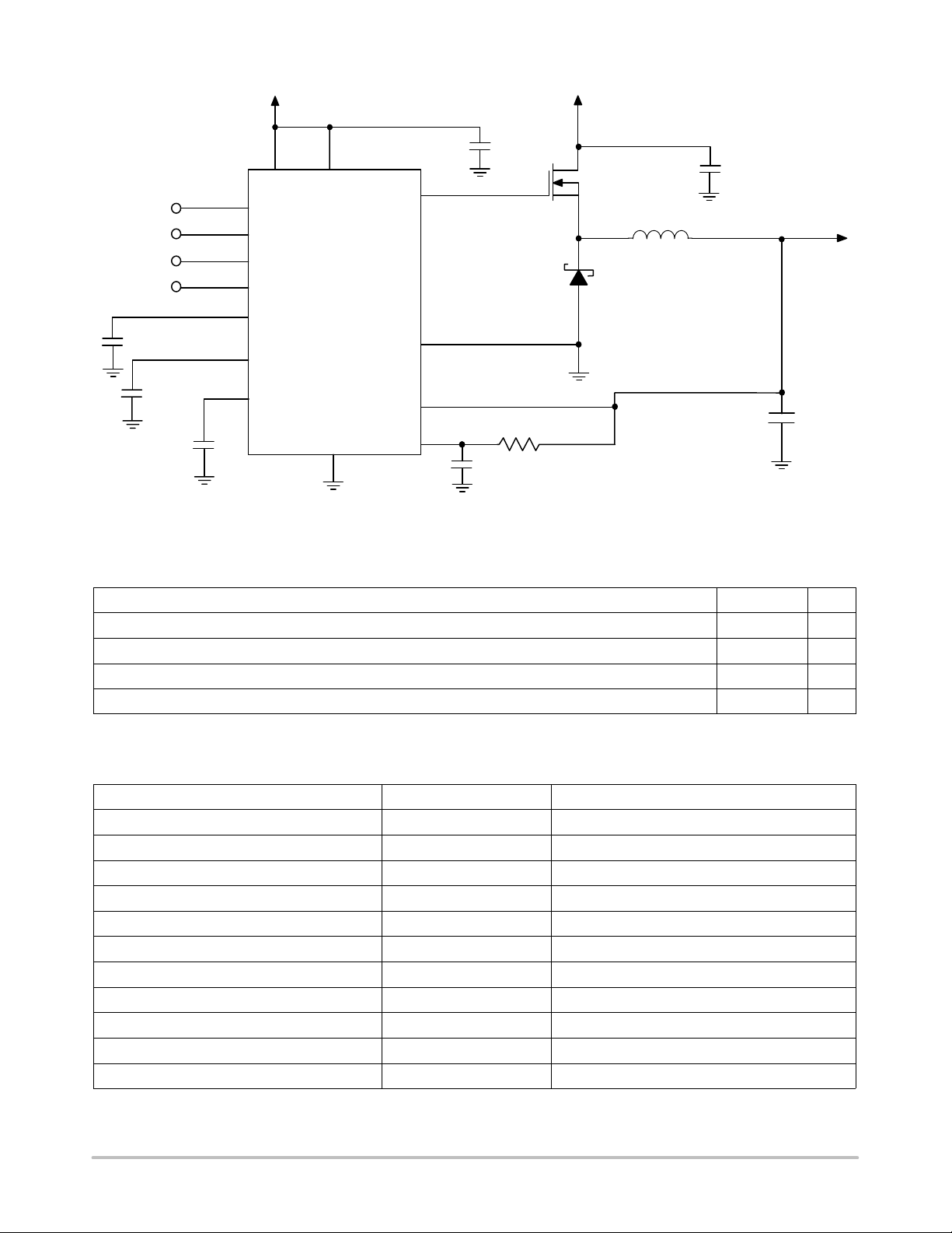
Figure 1. Application Diagram, Switching Power Supply for Core Logic – Pentium Processor with
MMX Technology
ABSOLUTE MAXIMUM RATINGS*
Rating Value Unit
Operating Junction Temperature, T
J
0 to 150 °C
Lead Temperature Soldering: Reflow: (SMD styles only) (Note 1.) 230 peak °C
Storage Temperature Range, T
S
–65 to +150 °C
ESD Susceptibility (Human Body Model) 2.0 kV
1. 60 second maximum above 183°C.
*The maximum package power dissipation must be observed.
ABSOLUTE MAXIMUM RATINGS
Pin Name Max Operating Voltage Max Current
V
CC1
V
CC2
SS 6.0 V/–0.3 V –100 µA
COMP 6.0 V/–0.3 V 200 µA
V
FB
C
OFF
V
FFB
V
– V
ID0
ID3
V
GATE
LGND 0 V 25 mA
PGND 0 V 100 mA DC/1.5 A peak
16 V/–0.3 V 25 mA DC/1.5 A peak
20 V/–0.3 V 20 mA DC/1.5 A peak
6.0 V/–0.3 V –0.2 µA
6.0 V/–0.3 V –0.2 µA
6.0 V/–0.3 V –0.2 µA
6.0 V/–0.3 V –50 µA
20 V/–0.3 V 100 mA DC/1.5 A peak
http://onsemi.com
2

CS5151H
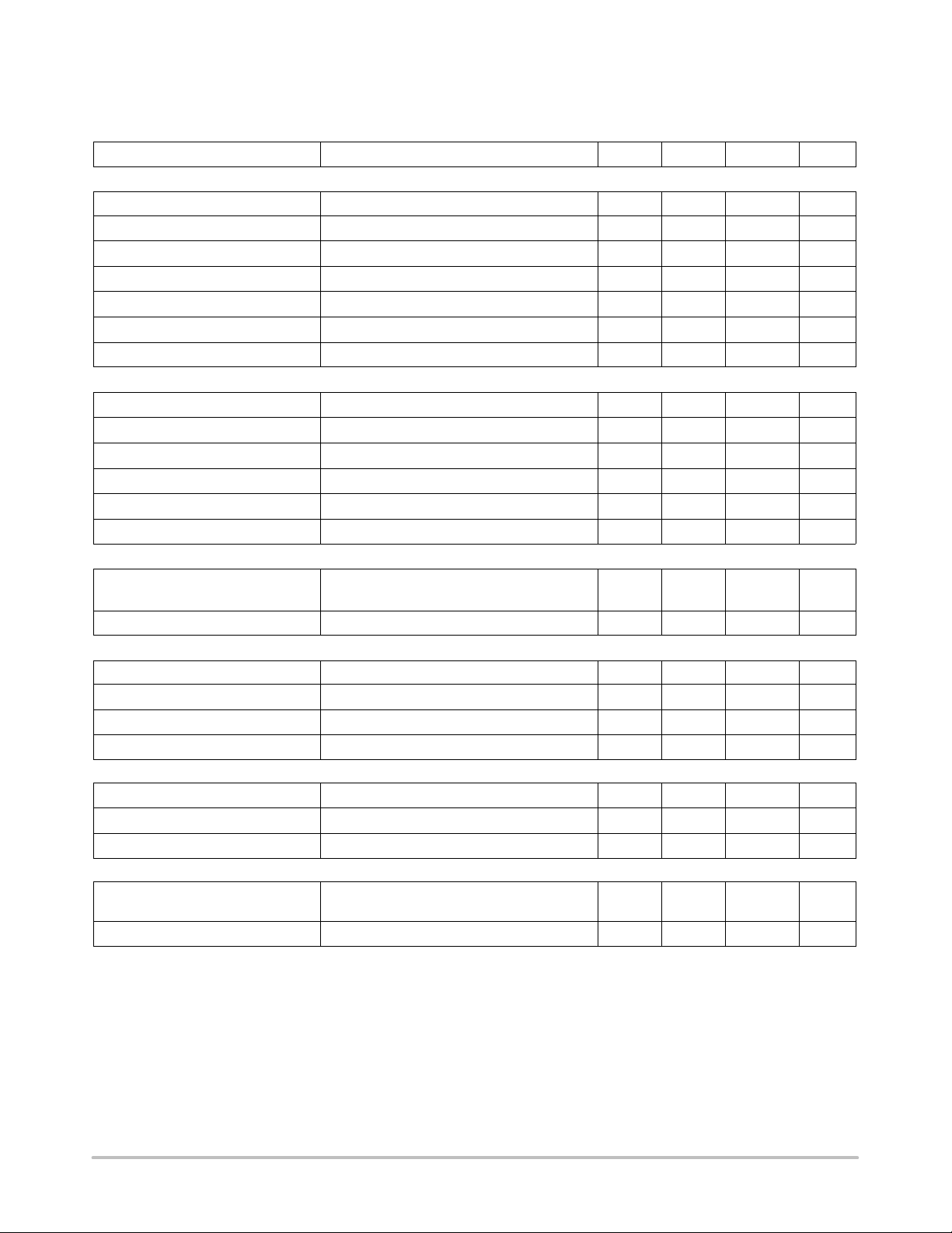
ELECTRICAL CHARACTERISTICS (0°C < T
DAC Code: V
Characteristic
ID2
= V
ID1
= V
ID0
= 1; V
ID3
= 0
CV
;
GATE
< +70°C; 0°C < TJ < +125°C; 8.0 V < V
A
= 1.0 nF; C
= 330 pF; CSS = 0.1 µF, unless otherwise specified.)
OFF
< 14 V; 5.0 V < V
CC1
Test Conditions Min Typ Max Unit
CC2
< 20 V;
Error Amplifier
Bias Current VFB = 0 V – 0.3 1.0 µA
V
FB
Open Loop Gain 1.25 V < V
< 4.0 V; Note 2. 50 60 – dB
COMP
Unity Gain Bandwidth Note 2. 500 3000 – kHz
COMP SINK Current V
COMP SOURCE Current V
COMP CLAMP Current V
= 1.5 V; VFB = 3.0 V; VSS > 2.0 V 0.4 2.5 8.0 mA
COMP
= 1.2 V; VFB = 2.7 V; VSS = 5.0 V 30 50 80 µA
COMP
= 0 V; VFB = 2.7 V 0.4 1.0 1.6 mA
COMP
COMP High Voltage VFB = 2.7 V; VSS = 5.0 V 4.0 4.3 5.0 V
COMP Low Voltage VFB = 3.0 V – 160 600 mV
PSRR 8.0 V < V
V
Monitor
CC1
< 14 V @ 1.0 kHz; Note 2. 60 85 – dB
CC1
Start Threshold Output switching 3.75 3.90 4.05 V
Stop Threshold Output not switching 3.70 3.85 4.00 V
Hysteresis Start–Stop – 50 – mV
DAC
Input Threshold V
Input Pull Up Resistance V
ID0,
ID0,
V
, V
, V
ID1
ID2
ID3
V
, V
, V
ID1
ID2
ID3
1.00 1.25 2.40 V
25 50 100 kΩ
Pull Up Voltage – 4.85 5.00 5.15 V
Accuracy (all codes except 1111) Measure VFB = V
V
ID3
V
ID2
V
ID1
V
ID0
, 25°C ≤ TJ ≤ 125°C – – 1.0 %
COMP
1 1 1 1 – 1.2191 1.2440 1.2689 V
1 1 1 0 – 2.1186 2.1400 2.1614 V
1 1 0 1 – 2.2176 2.2400 2.2624 V
1 1 0 0 – 2.3166 2.3400 2.3634 V
1 0 1 1 – 2.4156 2.4400 2.4644 V
1 0 1 0 – 2.5146 2.5400 2.5654 V
1 0 0 1 – 2.6136 2.6400 2.6664 V
1 0 0 0 – 2.7126 2.7400 2.7674 V
0 1 1 1 – 2.8116 2.8400 2.8684 V
0 1 1 0 – 2.9106 2.9400 2.9694 V
0 1 0 1 – 3.0096 3.0400 3.0704 V
0 1 0 0 – 3.1086 3.1400 3.1714 V
0 0 1 1 – 3.2076 3.2400 3.2724 V
0 0 1 0 – 3.3066 3.3400 3.3734 V
0 0 0 1 – 3.4056 3.4400 3.4744 V
0 0 0 0 – 3.5046 3.5400 3.5754 V
2. Guaranteed by design, not 100% tested in production.
http://onsemi.com
3
CS5151H
ELECTRICAL CHARACTERISTICS (continued) (0°C < T
5.0
V < V
< 20 V; DAC Code: V
CC2
ID2
= V
ID1
= V
ID0
=1; V
ID3
< +70°C; 0°C < TJ < +125°C; 8.0 V < V
A
=
CV
0;
GATE(L)
and CV
GATE(H)
= 1.0 nF; C
< 14 V;
CC1
= 330 pF; CSS = 0.1 µF, unless
OFF
otherwise specified.)
Characteristic
V
GATE
Out SOURCE Sat at 100 mA Measure V
Out SINK Sat at 100 mA Measure V
Out Rise Time 1.0 V < V
Out Fall Time 9.0 V > V
Test Conditions Min Typ Max Unit
CC2
GATE
GATE
GATE
– V
GATE
– V
PGND
< 9.0 V; V
> 1.0 V; V
CC1
CC1
= V
= 12 V – 30 50 ns
CC2
= V
= 12 V – 30 50 ns
CC2
– 1.2 2.0 V
– 1.0 1.5 V
Shoot–Through Current Note 3. – – 50 mA
V
Resistance Resistor to LGND. Note 3. 20 50 100 kΩ
GATE
V
Schottky LGND to V
GATE
@ 10 mA – 600 800 mV
GATE
Soft Start (SS)
Charge Time – 1.6 3.3 5.0 ms
Pulse Period – 25 100 200 ms
Duty Cycle (Charge Time /Pulse Period) × 100 1.0 3.3 6.0 %
COMP Clamp Voltage VFB = 0 V; VSS = 0 0.50 0.95 1.10 V
V
SS Fault Disable V
FFB
= Low 0.9 1.0 1.1 V
GATE
High Threshold – – 2.5 3.0 V
PWM Comparator
Transient Response
V
Bias Current V
FFB
V
= 0 to 5.0 V to V
FFB
V
= V
CC2
= 12 V
CC1
= 0 V – 0.3 – µA
FFB
= 9.0 V to 1.0 V;
GATE
– 100 125 ns
Supply Current
I
CC1
I
CC2
Operating I
Operating I
C
OFF
CC1
CC2
Normal Charge Time V
Extension Charge Time VSS = V
Discharge Current C
No Switching – 8.5 13.5 mA
No Switching – 1.6 3.0 mA
VFB = COMP = V
VFB = COMP = V
= 1.5 V; VSS = 5.0 V 1.0 1.6 2.2 µs
FFB
FFB
to 5.0 V; VFB > 1.0 V 5.0 – – mA
OFF
FFB
FFB
= 0 5.0 8.0 11.0 µs
– 8.0 13 mA
– 2.0 5.0 mA
Time Out Timer
Time Out Time
Fault Mode Duty Cycle V
VFB = V
Record V
FFB
; V
COMP
= 2.0 V;
FFB
Pulse High Duration
GATE
10 30 65 µs
= 0V 35 50 70 %
3. Guaranteed by design, not 100% tested in production.
http://onsemi.com
4

CS5151H
PACKAGE PIN DESCRIPTION
PACKAGE PIN #
16 Lead SO Narrow
1, 2, 3, 4 V
5 SS Soft Start Pin. A capacitor from this pin to LGND in conjunc-
6, 12 NC No Connection.
7 C
PIN SYMBOL FUNCTION
ID0–VID3
OFF
Voltage ID DAC input pins. These pins are internally pulled
up to 5.0 V providing logic ones if left open. The DAC range
is 2.14 V to 3.54 V with 100 mV increments. V
select the desired DAC output voltage. Leaving all 4 DAC
ID0
– V
ID3
input pins open results in a DAC output voltage of 1.244 V,
allowing for adjustable output voltage, using a traditional
resistor divider .
tion with internal 60 µA current source provides Soft Start
function for the controller. This pin disables fault detect function during Soft Start. When a fault is detected, the Soft Start
capacitor is slowly discharged by internal 2.0 µA current
source setting the time out before trying to restart the IC.
Charge/discharge current ratio of 30 sets the duty cycle for
the IC when the regulator output is shorted.
A capacitor from this pin to ground sets the time duration for
the on board one shot, which is used for the constant off time
architecture.
8 V
FFB
Fast feedback connection to the PWM comparator. This pin
is connected to the regulator output. The inner feedback loop
terminates on time.
9 V
10 V
CC2
GATE
Boosted power for the gate driver.
MOSFET driver pin capable of 1.5 A peak switching current.
11 PGND High current ground for the IC. The MOSFET driver is refer-
enced to this pin. Input capacitor ground and the anode of
the Schottky diode should be tied to this pin.
13 V
CC1
Input power for the IC.
14 LGND Signal ground for the IC. All control circuits are referenced to
this pin.
15 COMP Error amplifier compensation pin. A capacitor to ground
should be provided externally to compensate the amplifier.
16 V
FB
Error amplifier DC feedback input. This is the master voltage
feedback which sets the output voltage. This pin can be connected directly to the output or a remote sense trace.
http://onsemi.com
5
V
CC1
SS
V
ID0
V
ID1
V
ID2
V
ID3
V
FB
COMP
V
FFB
LGND
V
CC1
Comparator
–
+
3.90 V
3.85V
4 BIT
DAC
Slow Feedback
Fast Feedback
Monitor
Error
Amplifier
+
–
1.0 V
60 µA
2.0 µA
PWM
Comparator
–
+
–
+
V
FFB
Comparator
5.0 V
Low
2.5 V
CS5151H
SS Low
Comparator
–
+
0.7 V
SS High
Comparator
+
–
Maximum
On–Time
Timeout
Normal
Off–Time
Timeout
Extended
Off–Time
Timeout
Q
R
Q
S
FAULT
Latch
Off–Time
Timeout
FAULT
FAULT
R
S
PMW
Latch
Q
Q
GATE = ON
GATE = OFF
C
OFF
One Shot
R
Q
S
V
CC2
V
GATE
PGND
C
OFF
PWM COMP
Figure 2. Block Diagram
APPLICATIONS INFORMATION
THEORY OF OPERATION
V2 Control Method
The V2 method of control uses a ramp signal that is
generated by the ESR of the output capacitors. This ramp is
proportional to the AC current through the main inductor
and is offset by the value of the DC output voltage. This
control scheme inherently compensates for variation in
either line or load conditions, since the ramp signal is
generated from the output voltage itself. This control
scheme differs from traditional techniques such as voltage
mode, which generates an artificial ramp, and current mode,
which generates a ramp from inductor current.
COMP
Time–Out
Timer
(30 µs)
Edge Triggered
PWM
Comparator
+
C
–
Ramp
Signal
Error
Amplifier
Error
Signal
Figure 3. V2 Control Diagram
V
V
GATE
FFB
E
Output
Voltage
Feedback
V
FB
–
+
Reference
Voltage
http://onsemi.com
6

CS5151H
The V2 control method is illustrated in Figure 3. The
output voltage is used to generate both the error signal and
the ramp signal. Since the ramp signal is simply the output
voltage, it is a ffected by any change in the output regardless
of the origin of that change. The ramp signal also contains
the DC portion of the output voltage, which allows the
control circuit to drive the main switch to 0% or 100% duty
cycle as required.
A change in line voltage changes the current ramp in the
inductor, affecting the ramp signal, which causes the V
control scheme to compensate the duty cycle. Since the
change in inductor current modifies the ramp signal, as in
current mode control, the V2 control scheme has the same
advantages in line transient response.
A change in load current will have an affect on the output
voltage, altering the ramp signal. A load step immediately
changes the state of the comparator output, which controls
the main switch. Load transient response is determined only
by the comparator response time and the transition speed of
the main switch. The reaction time to an output load step has
no relation to the crossover frequency of the error signal
loop, as in traditional control methods.
The error signal loop can have a low crossover frequency,
since transient response is handled by the ramp signal loop.
The main purpose of this ‘slow’ feedback loop is to provide
DC accuracy. Noise immunity is significantly improved,
since the error amplifier bandwidth can be rolled off a t a lo w
frequency. Enhanced noise immunity improves remote
sensing of the output voltage, since the noise associated with
long feedback traces can be effectively filtered.
Line and load regulation are drastically improved because
there are two independent voltage loops. A voltage mode
controller relies on a change in the error signal to
compensate for a deviation in either line or load voltage.
This change in the error signal causes the output voltage to
change corresponding to the gain of the error amplifier,
which is normally specified as line and load regulation. A
current mode controller maintains fixed error signal under
deviation in the line voltage, since the slope of the ramp
signal changes, but still relies on a change in the error signal
for a deviation in load. The V
2
method of control maintains
a fixed error signal for both line and load variation, since the
ramp signal is affected by both line and load.
Constant Off Time
To maximize transient response, the CS5151H uses a
constant of f time method to control the rate of output pulses.
During normal operation, the off time of the high side switch
is terminated after a fixed period, set by the C
capacitor.
OFF
To maintain regulation, the V2 control loop varies switch on
time. The PWM comparator monitors the output voltage
ramp, and terminates the switch on time.
Constant off time provides a number of advantages.
Switch duty cycle can be adjusted from 0 to 100% on a pulse
by pulse basis when responding to transient conditions. Both
0% and 100% duty cycle operation can be maintained for
extended periods of time in response to load or line
transients. PWM slope compensation to avoid
sub–harmonic oscillations at high duty cycles is avoided.
Switch on time is limited by an internal 30 µs timer,
minimizing stress to the power components.
2
Programmable Output
The CS5151H is designed to provide two methods for
programming the output voltage of the power supply . A four
bit on board digital to analog converter (DAC) is used to
program the output voltage from 2.14 V to 3.54 V in 100 mV
steps, depending on the digital input code. If all four bits are
left open, the CS5151H enters adjust mode. In adjust mode,
the designer can choose any output voltage by using resistor
divider feedback to the V
FB
and V
pins, as in traditional
FFB
controllers. The CS5151H is specifically designed to be
upwards compatible with the CS5156H, which uses a five
bit DAC code.
Start Up
Until the voltage o n t he V
supply p in e xceeds t he 3 .9 V
CC1
monitor threshold, the Soft Start and gate pins are held low.
The FAULT latch is reset (no Fault condition). The output
of the error amplifier (COMP) is pulled up to 1.0 V by the
comparator clamp. When the V
pin exceeds the monitor
CC1
threshold, the GATE output is activated, and the Soft Start
capacitor begins charging. The GATE output will remain on,
enabling the NFET switch, until terminated by either the
PWM comparator, or the maximum on time timer.
If the maximum on time is exceeded before the regulator
output voltage achieves the 1.0 V level, the pulse is
terminated. The G ATE pin drives low for the duration of the
extended off time. This time is set by the time out timer and
is approximately equal to the maximum on time, resulting in
a 50% duty cycle. Then, the GATE pin will drive high, and
the cycle repeats.
When regulator output voltage achieves the 1.0 V level
present at the COMP pin, regulation has been achieved and
normal off time will ensue. The PWM comparator
terminates the switch on time, with off time set by the C
capacitor. The V2 control loop will adjust switch duty cycle
as required to ensure the regulator output voltage tracks the
output of the error amplifier.
The Soft Start and COMP capacitors will charge to their
final levels, providing a controlled turn on of the regulator
output. Regulator turn on time is determined by the COMP
capacitor charging to its final value. Its voltage is limited by
OFF
http://onsemi.com
7

CS5151H
o
the Soft Start COMP clamp and the voltage on the Soft Start
pin (see Figures 4 and 5).
M 250 µs
Trace 1– Regulator Output Voltage (1.0 V/div.)
Trace 2– Inductor Switching Node (2.0 V/div.)
Trace 3– 12 V Input (V
Trace 4– 5.0 V Input (1.0 V/div.)
Figure 4. CS5151H Demonstration Board Startup in
Response to Increasing 12 V and 5.0 V Input Voltages.
Extended Off Time is Followed by Normal Off Time
Operation when Output Voltage Achieves Regulation t
and V
CC1
) (5.0 V/div.)
CC2
the Error Amplifier Output.
M 10.0 µs
Trace 1– Regulator Output Voltage (5.0 V/div.)
Trace 2– Inductor Switching Node (5.0 V/div.)
Figure 6. CS5151H Demonstration Board Enable
Startup Waveforms
Normal Operation
During normal operation, switch off time is constant and
set by the C
capacitor. Switch on time is adjusted by the
OFF
V2 control loop to maintain regulation. This results in
changes in regulator switching frequency, duty cycle, and
output ripple in response to changes in load and line. Output
voltage ripple will be determined by inductor ripple current
working into the ESR of the output capacitors (see Figures
7 and 8).
M 2.50 ms
Trace 1– Regulator Output Voltage (1.0 V/div.)
Trace 3– COMP PIn (error amplifier output) (1.0 V/div.)
Trace 4– Soft Start Pin (2.0 V/div.)
Figure 5. CS5151H Demonstration Board Startup
Waveforms
If the input voltage rises quickly, or the regulator output
is enabled externally, output voltage will increase to the
level set by the error amplifier output more rapidly, usually
within a couple of cycles (see Figure 6).
http://onsemi.com
Trace 1– Regulator Output Voltage (10 mV/div.)
Trace 2– Inductor Switching Node (5.0 V/div.)
Figure 7. Peak–to–Peak Ripple on V
I
OUT
8
M 1.00 µs
= 0.5 A (Light Load)
OUT
= 2.8 V,
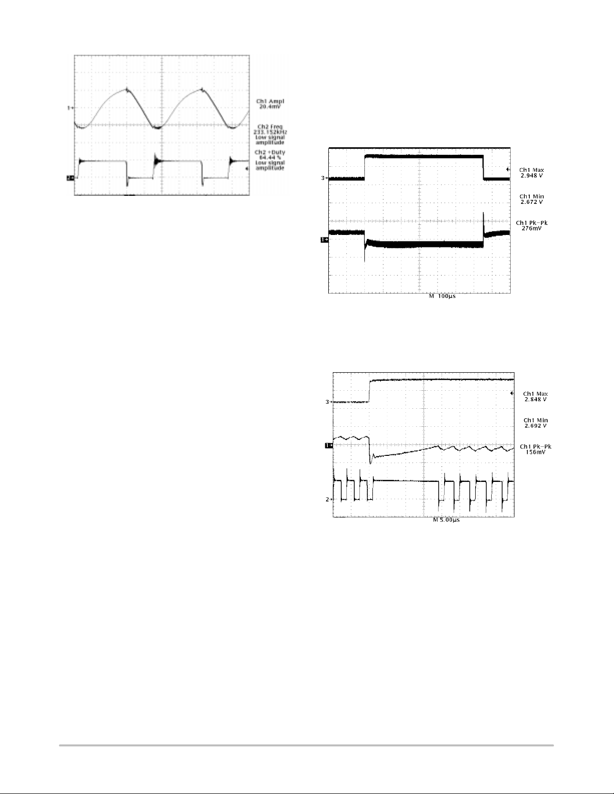
CS5151H
M 1.00 µs
Trace 1– Regulator Output Voltage (10 V/div.)
Trace 2– Inductor Switching Node (5.0 V/div.)
Figure 8. Peak–to–Peak Ripple on V
I
= 13 A (Heavy Load)
OUT
Transient Response
The CS5151H V2 control loop’s 100 ns reaction time
provides unprecedented transient response to changes in
input voltage or output current. Pulse by pulse adjustment of
duty cycle is provided to quickly ramp the inductor current
to the required level. Since the inductor current cannot be
changed instantaneously, regulation is maintained by the
output capacitor(s) during the time required to slew the
inductor current.
Overall load transient response is further improved
through a feature called “adaptive voltage positioning”. This
technique pre–positions the output capacitor’s voltage to
reduce total output voltage excursions during changes in
load.
Holding tolerance to 1.0% allows the error amplifier’s
reference voltage to be targeted +40 mV high without
compromising DC accuracy. A “droop resistor”,
implemented through a PC board trace, connects the error
amplifier’s feedback pin (V
) to the output capacitors and
FB
load and carries the output current. With no load, there is no
DC drop across this resistor, producing an output voltage
tracking the error amplifier’s, including the +40 mV offset.
When the full load current is delivered, an 80 mV drop is
developed across this resistor. This results in output voltage
being offset –40 mV low.
The result of adaptive voltage positioning is that
additional margin is provided for a load transient before
reaching the output voltage specification limits. When load
current suddenly increases from its minimum level, the
output capacitor is pre–positioned +40 mV. Conversely,
when load current suddenly decreases from its maximum
OUT
= 2.8 V,
level, the output capacitor is pre–positioned –40 mV (see
Figures 9, 10, and 11). For best transient response, a
combination of a number of high frequency and bulk output
capacitors are usually used.
If the maximum on time is exceeded while responding to
a sudden increase in load current, a normal off time occurs
to prevent saturation of the output inductor.
Trace 1– Regulator Output Voltage (1.0 V/div.)
Trace 2– Regulator Output Voltage (20 V/div.)
Figure 9. CS5151H Demonstration Board Response
to a 0.5 to 13 A Load Pulse (Output Set for 2.8 V)
Trace 1– Regulator Output Voltage (1.0 V/div.)
Trace 2– Inductor Switching Node (5.0 V/div.)
Trace 3– Output Current (0.5 to 13 Amps) (20 V/div.)
Figure 10. CS5151H Demonstration Board Response to
13 A Load Turn On (Output Set for 2.8 V). Upon
Completing a Normal Off Time, The V
Immediately Connects the Inductor to the Input
Voltage, Providing 100% Duty Cycle. Regulation is
Achieved in Less Than 20 s
2
Control Loop
http://onsemi.com
9
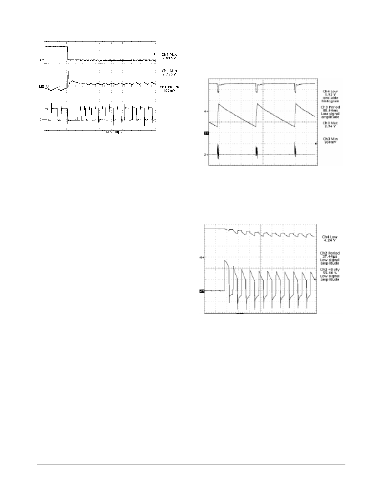
CS5151H
Trace 1– Regulator Output Voltage (1.0 V/div.)
Trace 2– Inductor Switching Node (5.0 V/div.)
Trace 3– Output Current (13 to 0,5 Amps) (20 mV/div.)
Figure 11. CS5151H Demonstration Board Response to
13 A Load Turn Off (Output Set for 2.8 V). V
Topology Immediately Connects Inductor to Ground,
Providing 0% Duty Cycle. Regulation is Achieved in
Less Than 10 s
PROTECTION AND MONITORING FEATURES
V
Monitor
CC1
To maintain predictable startup and shutdown
characteristics an internal V
monitor circuit is used to
CC1
prevent the part from operating below 3.75 V minimum
startup. The V
monitor comparator provides hysteresis
CC1
and guarantees a 3.70 V minimum shutdown threshold.
2
Control
traces than occurs with constant current limit protection (see
Figures 12 and 13).
If the short circuit condition is removed, output voltage
will rise above the 1.0 V level, preventing the FAULT latch
from being set, allowing normal operation to resume.
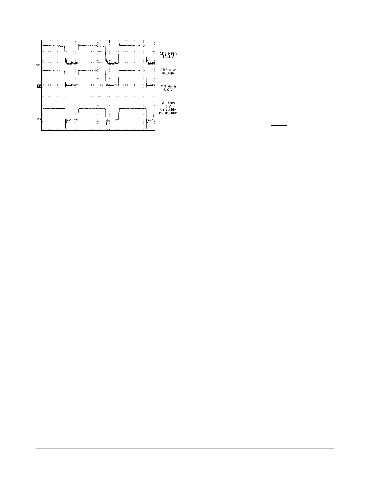
M 25.0 ms
Trace 4– 5.0 V Supply Voltage (2.0 V/div.)
Trace 3– Soft Start Timing Capacitor (1.0 V/div.)
Trace 2– Inductor Switching Node (2.0 V/div.)
Figure 12. CS5151H Demonstration Board Hiccup
Mode Short Circuit Protection. Gate Pulses are
Delivered While the Soft Start Capacitor Charges, and
Cease During Discharge
Short Circuit Protection
A lossless hiccup mode short circuit protection feature is
provided, requiring only the Soft Start capacitor to
implement. If a s hort c ircuit condition o ccurs ( V
the V
low comparator sets the F AULT latch. This causes
FFB
FFB
< 1.0 V),
the MOSFET to shut off, disconnecting the regulator from
it’s input voltage. The Soft Start capacitor is then slowly
discharged by a 2.0 µA current source until it reaches it’s
lower 0.7 V threshold. The regulator will then attempt to
restart normally, operating in it’s extended off time mode
with a 50% duty cycle, while the Soft Start capacitor is
charged with a 60 µA charge current.
If the short circuit condition persists, the regulator output
will not achieve the 1.0 V low V
comparator threshold
FFB
before the Soft Start capacitor is charged to it’s upper 2.5 V
threshold. If thi s happens the cycle will repeat itself until the
short is removed. The Soft Start charge/discharge current
ratio sets the duty cycle for the pulses (2.0 µA/60 µA =
3.3%), while actual duty cycle is half that due to the
extended off time mode (1.65%).
This protection feature results in less stress to the
regulator components, input power supply, and PC board
Trace 4– 5.0 V from PC Power Supply (2.0 V/div.)
Trace 2– Inductor Switching Node (2.0 V/div.)
Figure 13. Startup with Regulator Output Shorted
Overvoltage Protection
M 50.0 µs
Overvoltage protection (OVP) is provided as result of the
normal operation of the V
2
control topology and requires no
additional external components. The control loop responds
to an overvoltage condition within 100 ns, causing the
MOSFET to shut off, disconnecting the regulator from it’s
input voltage.
External Output Enable Circuit
On/off control of the regulator can be implemented
through two additional discrete components (see Figure 14).
http://onsemi.com
10

CS5151H
This circuit operates by pulling the Soft Start pin high, and
the V
Figure 14. Implementing Shutdown with the CS5151H
External Power Good Circuit
the use of four additional external components (see Figure
15). The threshold voltage of the Power Good signal can be
adjusted per the following equation:
the Power Good output to ground for regulator voltages less
than V
Figure 15. Implementing Power Good with the CS5151H
pin low, emulating a short circuit condition.
FFB
5.0 V
MMUN2111T1 (SOT–23)
5
SS
CS5151H
8
V
FFB
IN4148
Shutdown
Input
An optional Power Good signal can be generated through
V
Power Good
(R1 R2) 0.65 V
R2
This circuit provides an open collector output that drives
V
OUT
.
10 k
R1
R2
6.2 k
5.0 V
R3
10 k
PN3904
Power Good
PN3904
Power Good
CS5151H
M 2.50 ms
Trace 3 – 12 V Input (V
Trace 4– 5.0 V Input (2.0 V/div.)
Trace 1– Regulator Output Voltage (1.0 V/div.)
Trace 2– Power Good Signal (2.0 V/div.)
CC1
) and (V
) (10 V/div.)
CC2
Figure 16. CS5151H Demonstration Board During
Power Up. Power Good Signal is Activated when
Output Voltage Reaches 1.70 V.
Selecting External Components
The CS5151H can be used with a wide range of external
power components to optimize the cost and performance of
a particular design. The following information can be used
as general guidelines to assist in their selection.
NFET Power Transistors
Both logic level and standard MOSFETs can be used. The
reference designs derive gate drive from the 12 V supply
which is generally available in most computer systems and
use logic level MOSFETs. A charge pump may be easily
implemented to permit use of standard MOSFETs or support
5.0 V or 12 V only systems (maximum of 20 V). Multiple
MOSFETs may be paralleled to reduce losses and improve
efficiency and thermal management.
Voltage applied to the MOSFET gates depends on the
application circuit used. The gate driver output is specified
to drive to within 1.5 V of ground when in the low state and
to within 2.0 V of its bias supply when in the high state. In
practice, the MOSFET gate will be driven rail to rail due to
overshoot caused by the capacitive load it presents to the
controller IC. For the typical application where V
V
= 12 V and 5.0 V is used as the source for the regulator
CC2
CC1
=
output current, the following gate drive is provided;
V
12 V 5.0 V 7.0 V
GATE
(see Figure 17.)
http://onsemi.com
11
CS5151H
M 1.00 µs
Channel 3 = V
Channel 2– Inductor Switching Node
Figure 17. CS5151H Gate Drive Waveforms Depicting
The most important aspect of MOSFET performance is
RDSON, which effects regulator efficiency and MOSFET
thermal management requirements.
The power dissipated by the MOSFET and the Schottky
diode may be estimated as follows;
Switching MOSFET:
Schottky diode:
Duty Cycle =
VIN V
GATE
M1 = V
GATE
Power I
Power V
FORWARD
– 5.0 V
IN
Rail to Rail Swing
2
LOAD
FORWARD
RDSON duty cycle
V
V
OUT
(I
LOAD
I
LOAD
FORWARD
RDS
(
1 duty cycle
ON OF SYNCH FET
)
“Droop” Resistor for Adaptive Voltage Positioning
Adaptive voltage positioning is used to reduce output
voltage excursions during abrupt changes in load current.
Regulator output voltage is offset +40 mV when the
regulator is unloaded, and –40 mV at full load. This results
in increased margin before encountering minimum and
maximum transient voltage limits, allowing use of less
capacitance on the regulator output (see Figure 9).
To implement adaptive voltage positioning, a “droop”
resistor must be connected between the output inductor and
output capacitors and load. This is normally implemented by
a PC board trace of the following value:
R
DROOP
80 mV
I
MAX
Adaptive voltage positioning can be disabled for
improved DC regulation by connecting the VFB pin directly
to the load using a separate, non–load current carrying
circuit trace.
Input and Output Capacitors
These components must be selected and placed carefully
to yield optimal results. Capacitors should be chosen to
provide acceptable ripple on the input supply lines and
regulator output voltage. Key specifications for input
capacitors are their ripple rating, while ESR is important for
output capacitors. For best transient response, a combination
of low value/high frequency and bulk capacitors placed
close to the load will be required.
)
Output Inductor
The inductor should be selected based on its inductance,
current capability, and DC resistance. Increasing the
inductor value will decrease output voltage ripple, but
degrade transient response.
Off Time Capacitor (C
The C
When the V
the C
timing capacitor sets the regulator off time:
OFF
T
OFF
pin is less than 1.0 V, the current charging
FFB
capacitor is reduced. The extended off time can be
OFF
OFF
C
)
OFF
4848.5
calculated as follows:
T
C
OFF
Off time will be determined by either the T
OFF
24,242.5
time, or the
OFF
time out timer, whichever is longer.
The preceding equations for duty cycle can also be used
to calculate the regulator switching frequency and select the
C
timing capacitor:
OFF
C
OFF
Perioid (1 duty cycle
4848.5
)
where:
Period
switching frequency
1
http://onsemi.com
THERMAL MANAGEMENT
Thermal Considerations for Power
MOSFETs and Diodes
In order to maintain good reliability, the junction
temperature of the semiconductor components should be
kept to a maximum of 150°C or lower. The thermal
impedance (junction to ambient) required to meet this
requirement can be calculated as follows:
Thermal Impedance
T
JUNCTION(MAX)
Power
T
AMBIENT
A heatsink may be added to TO–220 components to
reduce their thermal impedance. A number of PC board
layout techniques such as thermal vias and additional copper
foil area can be used to improve the power handling
capability of surface mount components.
12
CS5151H
EMI Management
As a consequence of large currents being turned on and off
at high frequency, switching regulators generate noise as a
consequence of their normal operation. When designing for
compliance with EMI/EMC regulations, additional
components may be added to reduce noise emissions. These
components are not required for regulator operation and
experimental results may allow them to be eliminated. The
input filter inductor may not be required because bulk filter
and bypass capacitors, as well as other loads located on the
board will tend to reduce regulator di/dt effects on the circuit
board and input power supply. Placement of the power
component to minimize routing distance will also help to
reduce emissions.
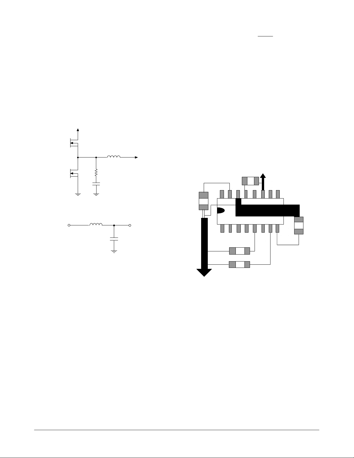
2.0 µH
33 Ω
1000 pF
Figure 18. Filter Components
R
TRACE
80 mV
I
MAX
This causes the output voltage to be +40 mV with no
load, and –40 mV with a full load, improving regulator
transient response. This trace must be wide enough to
carry the full output current. (T ypical trace is 1.0 inch
long, 0.17 inch wide). Care should be taken to
minimize any additional losses after the feedback
connection point to maximize regulation.
7. If DC regulation is to be optimized (at the expense of
degraded transient regulation), adaptive voltage
positioning can be disabled by connecting to V
directly to the load with a separate trace (remote
sense).
8. Place 5.0 V input capacitors close to the switching
MOSFET.
Route gate drive signals V
(pin 10) with a trace
GATE
that is a minimum of 0.025 inches wide.
To the negative terminal
of the input capacitors
1.0 µF
V
COMP
V
CC
0.1 µF
15 11
FB
pin
2.0 µH
+
1200 pF × 3.0/16 V
Figure 19. Input Filter
Layout Guidelines
1. Place 12 V filter capacitor next to the IC and connect
capacitor ground to pin 11 (PGND).
2. Connect pin 11 (PGND) with a separate trace to the
ground terminals of the 5.0 V input capacitors.
3. Place fast feedback filter capacitor next to pin 8 (V
and connect it’s ground terminal with a separate, wide
trace directly to pin 14 (LGND).
4. Connect the ground terminals of the Compensation
capacitor directly to the ground of the fast feedback
filter capacitor to prevent common mode noise from
effecting the PWM comparator.
5. Place the output filter capacitor(s) as close to the load
as possible and connect the ground terminal to pin 14
(LGND).
6. To implement adaptive voltage positioning, connect
both slow and fast feedback pins 16 (V
(V
) to the regulator output right at the inductor
FFB
) and 8
FB
terminal. Connect inductor to the output capacitors via
a trace with the following resistance:
FFB
8
5
SOFT START
OFF TIME
To the negative terminal of the output capacitors
Figure 20. Layout Guidelines
100 pF
V
FFB
)
http://onsemi.com
13

5.0V
CS5151H
MBRS
120
0.1 µF
0.1 µF
330 pF
0.33 µF
MBRS120
MBRS120
1.0 µF
1.0 µF
V
CC1
V
ID0
V
ID1
V
ID2
V
ID3
C
OFF
V
CC2
CS5151H
V
GATE
Si4410DY
MBR1535CT
+
2
1,3
PGND
SS
COMP
LGND
V
FB
V
FFB
3.3 k
100 pF
Figure 21. Additional Application Diagram, 5.0 V to 3.3 V/10 A Converter
12 V
3.3 V
100 µF/10 V × 3
Tantalum
3.0 µH
3.3 V/10 A
+
100 µF/10 V × 3
Tantalum
1.0 µF
+
CC1
V
CC2
CS5151H
V
GATE
V
FB
Si9410
MBR1535CT
2
1,3
V
V
ID0
V
ID1
V
ID2
V
ID3
C
OFF
330 pF
0.1 µF
0.1 µF
SS
COMP
LGND
0.33 µF
PGND
V
FFB
3.3 k
100 pF
Figure 22. Additional Application Diagram, 3.3 V to 2.5 V/7.0 A Converter with 12 V Bias
33 µF/25 V × 3
Tantalum
5.0 µH
+
2.5 V/7.0 A
100 µF/10 V × 2
Tantalum
http://onsemi.com
14

MBRS
120
0.1 µF
CS5151H
5.0V
MBRS120
2
1,3
+
100 µF/10 V × 3
Tantalum
3.0 µH
10 Ω
MBRS120
1.0 µF
1.0 µF
V
CC1
V
ID0
V
ID1
V
ID2
V
ID3
C
OFF
V
CC2
CS5151H
V
GATE
V
FB
Si4410
MBR1535CT
330 pF
0.1 µF
SS
COMP
LGND
0.33 µF
PGND
V
FFB
3.3 k
100 pF
Figure 23. Additional Application Diagram, 5.0 V to 3.3 V/10 A Converter with Current Sharing
Remote
Sense
3.3 V/10 A
100 µF/10 V × 3
+
Tantalum
Connect to other
circuits for current
sharing
http://onsemi.com
15

–T–
–A–
16 9
–B–
18
G
K
C
SEATING
PLANE
D
16 PL
0.25 (0.010) A
M
S
B
T
S
CS5151H
PACKAGE DIMENSIONS
SO–16
D SUFFIX
CASE 751B–05
ISSUE J
8 PLP
M
0.25 (0.010) B
M
S
X 45
R
NOTES:
1. DIMENSIONING AND TOLERANCING PER ANSI
Y14.5M, 1982.
2. CONTROLLING DIMENSION: MILLIMETER.
3. DIMENSIONS A AND B DO NOT INCLUDE
MOLD PROTRUSION.
4. MAXIMUM MOLD PROTRUSION 0.15 (0.006)
PER SIDE.
5. DIMENSION D DOES NOT INCLUDE DAMBAR
PROTRUSION. ALLOWABLE DAMBAR
PROTRUSION SHALL BE 0.127 (0.005) TOTAL
IN EXCESS OF THE D DIMENSION AT
MAXIMUM MATERIAL CONDITION.
F
J
DIM MIN MAX MIN MAX
A 9.80 10.00 0.386 0.393
B 3.80 4.00 0.150 0.157
C 1.35 1.75 0.054 0.068
D 0.35 0.49 0.014 0.019
F 0.40 1.25 0.016 0.049
G 1.27 BSC 0.050 BSC
J 0.19 0.25 0.008 0.009
K 0.10 0.25 0.004 0.009
M 0 7 0 7
P 5.80 6.20 0.229 0.244
R 0.25 0.50 0.010 0.019
INCHESMILLIMETERS
PACKAGE THERMAL DATA
Parameter
R
Θ
JC
R
Θ
JA
V2 is a trademark of Switch Power, Inc.
Pentium is a registered trademark and MMX is a trademark of Intel Corporation.
ON Semiconductor and are trademarks of Semiconductor Components Industries, LLC (SCILLC). SCILLC reserves the right to make changes without
further notice to any products herein. SCILLC makes no warranty, representation or guarantee regarding the suitability of its products for any particular
purpose, nor does SCILLC assume any liability arising out of the application or use of any product or circuit, and specifically disclaims any and all liability,
including without limitation special, consequential or incidental damages. “Typical” parameters which may be provided in SCILLC data sheets and/or
specifications can and do vary in different applications and actual performance may vary over time. All operating parameters, including “Typicals” must be
validated for each customer application by customer’s technical experts. SCILLC does not convey any license under its patent rights nor the rights of others.
SCILLC products are not designed, intended, or authorized for use as components in systems intended for surgical implant into the body, or other applications
intended to support or sustain life, or for any other application in which the failure of the SCILLC product could create a situation where personal injury or
death may occur. Should Buyer purchase or use SCILLC products for any such unintended or unauthorized application, Buyer shall indemnify and hold
SCILLC and its officers, employees, subsidiaries, affiliates, and distributors harmless against all claims, costs, damages, and expenses, and reasonable
attorney fees arising out of, directly or indirectly, any claim of personal injury or death associated with such unintended or unauthorized use, even if such claim
alleges that SCILLC was negligent regarding the design or manufacture of the part. SCILLC is an Equal Opportunity/Affirmative Action Employer.
Typical 28 °C/W
Typical 115 °C/W
16–SO Unit
PUBLICATION ORDERING INFORMATION
NORTH AMERICA Literature Fulfillment:
Literature Distribution Center for ON Semiconductor
P.O. Box 5163, Denver, Colorado 80217 USA
Phone: 303–675–2175 or 800–344–3860 Toll Free USA/Canada
Fax: 303–675–2176 or 800–344–3867 Toll Free USA/Canada
Email: ONlit@hibbertco.com
Fax Response Line: 303–675–2167 or 800–344–3810 Toll Free USA/Canada
N. American Technical Support: 800–282–9855 Toll Free USA/Canada
EUROPE: LDC for ON Semiconductor – European Support
German Phone: (+1) 303–308–7140 (Mon–Fri 2:30pm to 7:00pm CET)
Email: ONlit–german@hibbertco.com
French Phone: (+1) 303–308–7141 (Mon–Fri 2:00pm to 7:00pm CET)
Email: ONlit–french@hibbertco.com
English Phone: (+1) 303–308–7142 (Mon–Fri 12:00pm to 5:00pm GMT)
Email: ONlit@hibbertco.com
EUROPEAN TOLL–FREE ACCESS*: 00–800–4422–3781
*Available from Germany, France, Italy, UK, Ireland
CENTRAL/SOUTH AMERICA:
Spanish Phone: 303–308–7143 (Mon–Fri 8:00am to 5:00pm MST)
Email: ONlit–spanish@hibbertco.com
ASIA/PACIFIC: LDC for ON Semiconductor – Asia Support
Phone: 303–675–2121 (Tue–Fri 9:00am to 1:00pm, Hong Kong Time)
Toll Free from Hong Kong & Singapore:
001–800–4422–3781
Email: ONlit–asia@hibbertco.com
JAPAN: ON Semiconductor, Japan Customer Focus Center
4–32–1 Nishi–Gotanda, Shinagawa–ku, Tokyo, Japan 141–0031
Phone: 81–3–5740–2745
Email: r14525@onsemi.com
ON Semiconductor Website: http://onsemi.com
For additional information, please contact your local
Sales Representative.
http://onsemi.com
16
CS5151H/D
 Loading...