

查询1SMA10供应商
1SMA5.0AT3 Series
400 Watt Peak Power Zener
Transient Voltage Suppressors
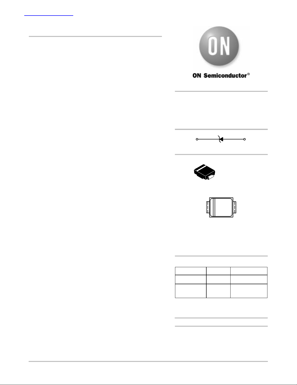
Unidirectional*
The SMA series is designed to protect voltage sensitive
components from high voltage, high energy transients. They have
excellent clamping capability, high surge capability, low zener
impedance and fast response time. The SMA series is supplied in
ON Semiconductor’s exclusive, cost-effective, highly reliable
Surmetic package and is ideally suited for use in communication
systems, automotive, numerical controls, process controls, medical
equipment, business machines, power supplies and many other
industrial/consumer applications.
Specification Features
• Working Peak Reverse Voltage Range − 5.0 V to 78 V
• Standard Zener Breakdown Voltage Range − 6.7 V to 91.25 V
• Peak Power − 400 W @ 1 ms
• ESD Rating of Class 3 (> 16 KV) per Human Body Model
• Response Time is Typically < 1 ns
• Flat Handling Surface for Accurate Placement
• Package Design for Top Slide or Bottom Circuit Board Mounting
• Low Profile Package
• Pb−Free Packages are Available
http://onsemi.com
PLASTIC SURFACE MOUNT
ZENER OVERVOLTAGE
TRANSIENT SUPPRESSORS
5.0 − 78 V, 400 W PEAK POWER
CATHODE ANODE
SMA
CASE 403D
PLASTIC
MARKING DIAGRAM
Mechanical Characteristics
CASE:
Void-free, transfer-molded plastic
FINISH: All external surfaces are corrosion resistant and leads are
readily solderable
MAXIMUM CASE TEMPERATURE FOR SOLDERING PURPOSES:
260°C for 10 Seconds
POLARITY: Cathode indicated by molded polarity notch or polarity
band
MOUNTING POSITION: Any
xx
LLYWW
xx = Specific Device Code
LL = Assembly Location
Y = Year
WW = Work Week
ORDERING INFORMATION
Device Package Shipping
1SMAxxAT3 SMA 5000/Tape & Reel
1SMAxxAT3G SMA
†For information on tape and reel specifications,
including part orientation and tape sizes, please
refer to our Tape and Reel Packaging Specifications
Brochure, BRD8011/D.
Individual devices are listed on page 3 of this data sheet.
*Please see 1SMA10CAT3 to 1SMA78CAT3 for
Bidirectional devices.
= (See Table on Page
5000/Tape & Reel
(Pb−Free)
3)
†
Semiconductor Components Industries, LLC, 2004
April, 2004 − Rev. 6
1 Publication Order Number:
1SMA5.0AT3/D
1SMA5.0AT3 Series
MAXIMUM RATINGS
Rating Symbol Value Unit
Peak Power Dissipation (Note 1) @ TL = 25°C, Pulse Width = 1 ms P
DC Power Dissipation @ TL = 75°C
PK
P
D
Measured Zero Lead Length (Note 2)
Derate Above 75°C
Thermal Resistance from Junction to Lead
DC Power Dissipation (Note 3) @ TA = 25°C
R
JL
P
D
Derate Above 25°C
Thermal Resistance from Junction to Ambient
Forward Surge Current (Note 4) @ TA = 25°C I
Operating and Storage Temperature Range TJ, T
R
FSM
JA
stg
Maximum ratings are those values beyond which device damage can occur. Maximum ratings applied to the device are individual stress limit
values (not normal operating conditions) and are not valid simultaneously . If these limits are exceeded, device functional operation is not implied,
damage may occur and reliability may be affected.
1. 10 X 1000 s, non−repetitive
2. 1″ square copper pad, FR−4 board
3. FR−4 board, using ON Semiconductor minimum recommended footprint, as shown in 403B case outline dimensions spec.
4. 1/2 sine wave (or equivalent square wave), PW = 8.3 ms, duty cycle = 4 pulses per minute maximum.
400 W
1.5
20
50
0.5
4.0
250
W
mW/°C
°C/W
W
mW/°C
°C/W
40 A
−65 to +150 °C
I
I
F
V
VCV
BR
RWM
I
V
R
F
I
T
I
PP
V
Uni−Directional TVS
5. 1/2 sine wave or equivalent, PW = 8.3 ms, non−repetitive
duty cycle.
ELECTRICAL CHARACTERISTICS
(TA = 25°C unless otherwise noted, VF = 3.5 V Max. @
I
= 30 A for all types) (Note 5)
F
Symbol
I
PP
V
C
V
RWM
I
R
V
BR
I
T
I
F
V
F
Maximum Reverse Peak Pulse Current
Clamping Voltage @ I
Working Peak Reverse Voltage
Maximum Reverse Leakage Current @ V
Breakdown Voltage @ I
Test Current
Forward Current
Forward Voltage @ I
Parameter
PP
T
F
RWM
http://onsemi.com
2

ELECTRICAL CHARACTERISTICS
V
Devi
1SMA5.0AT3 Series
Device
ce
Marking
RWM
(Note 6)
I
R
Volts A
@ V
RWM
Breakdown Voltage VC @ I
V
(Volts) (Note 7) @ I
BR
T
Min Nom Max mA
PP
V
C
Volts Amps
1SMA5.0AT3 QE 5.0 400 6.4 6.7 7.0 10 9.2 43.5
1SMA6.0AT3 QG 6.0 400 6.67 7.02 7.37 10 10.3 38.8
1SMA6.5AT3 QK 6.5 250 7.22 7.6 7.98 10 11.2 35.7
1SMA7.0AT3 QM 7.0 250 7.78 8.19 8.6 10 12.0 33.3
1SMA7.5AT3 QP 7.5 50 8.33 8.77 9.21 1 12.9 31.0
1SMA8.0AT3 QR 8.0 25 8.89 9.36 9.83 1 13.6 29.4
1SMA8.5AT3 QT 8.5 5.0 9.44 9.92 10.4 1 14.4 27.8
1SMA9.0AT3 QV 9.0 2.5 10 10.55 11.1 1 15.4 26.0
1SMA10AT3 QX 10 2.5 11.1 11.7 12.3 1 17.0 23.5
1SMA11AT3 QZ 11 2.5 12.2 12.85 13.5 1 18.2 22.0
1SMA12AT3 RE 12 2.5 13.3 14.0 14.7 1 19.9 20.1
1SMA13AT3 RG 13 2.5 14.4 15.15 15.9 1 21.5 18.6
1SMA14AT3 RK 14 2.5 15.6 16.4 17.2 1 23.2 17.2
1SMA15AT3 RM 15 2.5 16.7 17.6 18.5 1 24.4 16.4
1SMA16AT3, G* RP 16 2.5 17.8 18.75 19.7 1 26.0 15.4
1SMA17AT3 RR 17 2.5 18.9 19.9 20.9 1 27.6 14.5
1SMA18AT3, G* RT 18 2.5 20 21.05 22.1 1 29.2 13.7
1SMA20AT3 RV 20 2.5 22.2 23.35 24.5 1 32.4 12.3
1SMA22AT3 RX 22 2.5 24.4 25.65 26.9 1 35.5 11.3
1SMA24AT3 RZ 24 2.5 26.7 28.1 29.5 1 38.9 10.3
1SMA26AT3 SE 26 2.5 28.9 30.4 31.9 1 42.1 9.5
1SMA28AT3 SG 28 2.5 31.1 32.75 34.4 1 45.4 8.8
1SMA30AT3 SK 30 2.5 33.3 35.05 36.8 1 48.4 8.3
1SMA33AT3 SM 33 2.5 36.7 38.65 40.6 1 53.3 7.5
1SMA36AT3 SP 36 2.5 40 42.1 44.2 1 58.1 6.9
1SMA40AT3 SR 40 2.5 44.4 46.75 49.1 1 64.5 6.2
1SMA43AT3 ST 43 2.5 47.8 50.3 52.8 1 69.4 5.8
1SMA45AT3 SV 45 2.5 50 52.65 55.3 1 72.2 5.5
1SMA48AT3 SX 48 2.5 53.3 56.1 58.9 1 77.4 5.2
1SMA51AT3 SZ 51 2.5 56.7 59.7 62.7 1 82.4 4.9
1SMA54AT3 TE 54 2.5 60 63.15 66.3 1 87.1 4.6
1SMA58AT3 TG 58 2.5 64.4 67.8 71.5 1 93.6 4.3
1SMA60AT3 TK 60 2.5 66.7 70.2 73.7 1 96.8 4.1
1SMA64AT3 TM 64 2.5 71.1 74.85 78.6 1 103 3.9
1SMA70AT3 TP 70 2.5 77.8 81.9 86.0 1 113 3.5
1SMA75AT3 TR 75 2.5 83.3 87.7 92.1 1 121 3.3
1SMA78AT3 TS 78 2.5 86.7 91.25 95.8 1 126 3.2
6. A transient suppressor is normally selected according to the working peak reverse voltage (V
the DC or continuous peak operating voltage level
), which should be equal to or greater than
RWM
7. VBR measured at pulse test current IT at an ambient temperature of 25°C
8. Surge current waveform per Figure 2 and derate per Figure 3
*The “G” suffix indicates Pb−Free package available.
(Note 8)
I
PP
http://onsemi.com
3

1SMA5.0AT3 Series
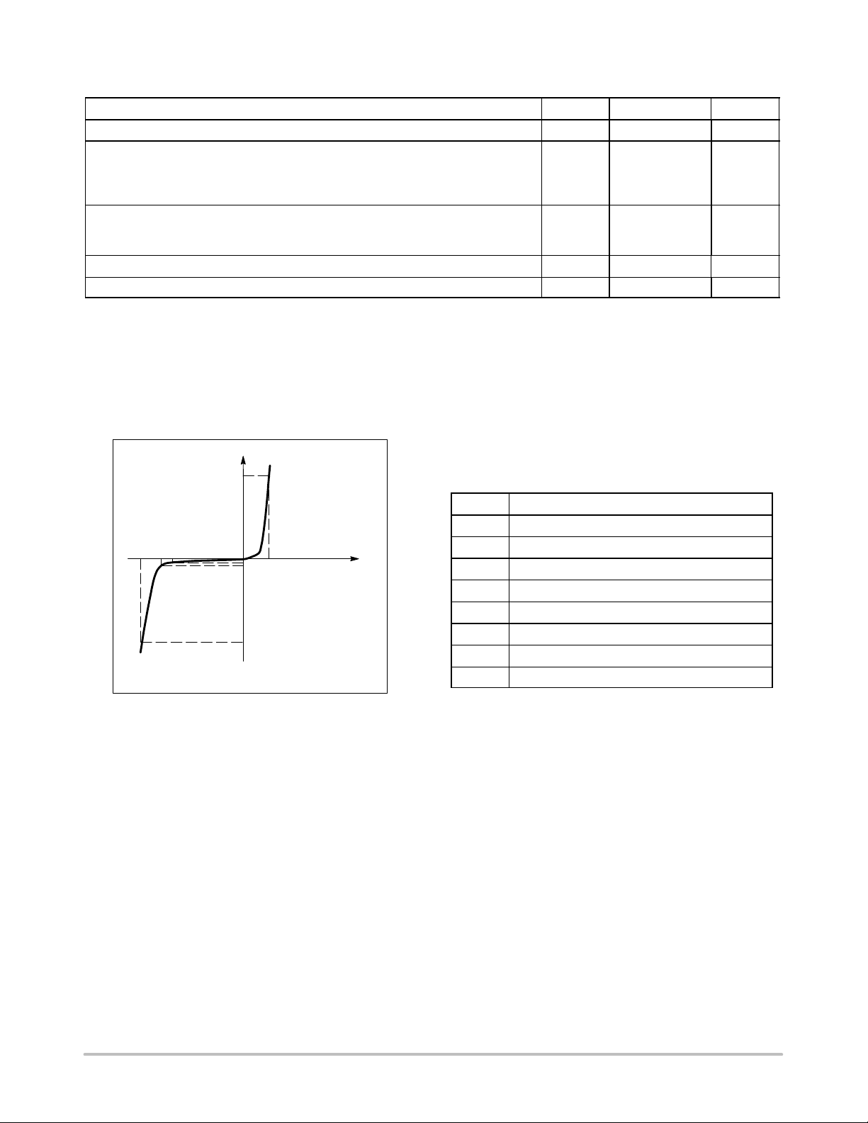
RATING AND TYPICAL CHARACTERISTIC CURVES
100
10
, PEAK POWER (kW)
1
pk
P
0.1
−4
10
120
100
80
60
120
T
= 25°C
A
PW (I
) IS DEFINED AS THE
D
POINT WHERE THE PEAK CURRENT
DECAYS TO 50% OF I
HALF VALUE − Ipp/2
10/1000 s WAVEFORM
AS DEFINED BY R.E.A.
t, TIME (ms)
0.010.001
, PULSE WIDTH (ms)
t
P
0.1 1 10
NONREPETITIVE
PULSE WAVEFORM
SHOWN IN FIGURE 2.
T
= 25°C
A
≤ 10 s
100
PEAK VALUE
80
I
ppm
60
40
, PEAK PULSE CURRENT (%)
ppm
I
20
t
d
0
01 2 3 4
Figure 1. Pulse Rating Curve Figure 2. Pulse Waveform
10,000
10 x 1000 WAVEFORM
AS DEFINED BY R.E.A.
1,000
MEASURED AT
ZERO BIAS
.
pp
T
= 25°C
J
f = 1 MHz
= 50 mV
V
sig
5
p−p
40
PEAK POWER OR CURRENT
PEAK PULSE DERATING IN % OF
20
0
0 40 80 120 160
T
, AMBIENT TEMPERATURE (°C)
A
Figure 3. Pulse Derating Curve Figure 4. Typical Junction Capacitance
6
5
4
3
2
1
, MAXIMUM POWER DISSIPATION (WATTS)
D
P
0
@ TA = 25°C
P
= 0.5 W
D
0
100
C, CAPACITANCE (pF)
10
200
1 2 5 10 20 50 100 200
@ TL = 75°C
P
= 1.5 W
D
25 75 125
50 100 150
T, TEMPERATURE (°C)
MEASURED AT
STAND−OFF
VOLTAGE, V
V
WM
, BREAKDOWN VOLTAGE (VOLTS)
(BR)
Figure 5. Steady State Power Derating
http://onsemi.com
4

S
A
DB
POLARITY INDICATOR OPTIONAL
AS NEEDED
1SMA5.0AT3 Series
SMA
CASE 403D−02
ISSUE A
C
NOTES:
1. DIMENSIONING AND TOLERANCING PER ANSI
Y14.5M, 1982.
2. CONTROLLING DIMENSION: INCH.
3. 403D−01 OBSOLETE, NEW STANDARD IS
403D−02.
DIM MIN MAX MIN MAX
A 0.160 0.180 4.06 4.57
B 0.090 0.115 2.29 2.92
C 0.075 0.095 1.91 2.41
D 0.050 0.064 1.27 1.63
H 0.002 0.006 0.05 0.15
J 0.006 0.016 0.15 0.41
K 0.030 0.060 0.76 1.52
S 0.190 0.220 4.83 5.59
MILLIMETERSINCHES
K
J
H
SOLDERING FOOTPRINT*
4.0
0.157
2.0
0.0787
2.0
0.0787
mm
SCALE 8:1
*For additional information on our Pb−Free strategy and soldering
details, please download the ON Semiconductor Soldering and
Mounting Techniques Reference Manual, SOLDERRM/D.
inches
http://onsemi.com
5

1SMA5.0AT3 Series
SURMETIC is a trademark of Semiconductor Components Industries, LLC.
ON Semiconductor and are registered trademarks of Semiconductor Components Industries, LLC (SCILLC). SCILLC reserves the right to make changes without further notice
to any products herein. SCILLC makes no warranty, representation or guarantee regarding the suitability of its products for any particular purpose, nor does SCILLC assume any liability
arising out of the application or use of any product or circuit, and specifically disclaims any and all liability, including without limitation special, consequential or incidental damages.
“Typical” parameters which may be provided in SCILLC data sheets and/or specifications can and do vary in different applications and actual performance may vary over time. All
operating parameters, including “Typicals” must be validated for each customer application by customer’s technical experts. SCILLC does not convey any license under its patent rights
nor the rights of others. SCILLC products are not designed, intended, or authorized for use as components in systems intended for surgical implant into the body, or other applications
intended to support or sustain life, or for any other application in which the failure of the SCILLC product could create a situation where personal injury or death may occur. Should
Buyer purchase or use SCILLC products for any such unintended or unauthorized application, Buyer shall indemnify and hold SCILLC and its officers, employees, subsidiaries, affiliates,
and distributors harmless against all claims, costs, damages, and expenses, and reasonable attorney fees arising out of, directly or indirectly, any claim of personal injury or death
associated with such unintended or unauthorized use, even if such claim alleges that SCILLC was negligent regarding the design or manufacture of the part. SCILLC is an Equal
Opportunity/Affirmative Action Employer. This literature is subject to all applicable copyright laws and is not for resale in any manner.
PUBLICATION ORDERING INFORMATION
LITERATURE FULFILLMENT:
Literature Distribution Center for ON Semiconductor
P.O. Box 5163, Denver, Colorado 80217 USA
Phone: 303−675−2175 or 800−344−3860 Toll Free USA/Canada
Fax: 303−675−2176 or 800−344−3867 Toll Free USA/Canada
Email: orderlit@onsemi.com
N. American Technical Support: 800−282−9855 Toll Free
USA/Canada
Japan: ON Semiconductor, Japan Customer Focus Center
2−9−1 Kamimeguro, Meguro−ku, Tokyo, Japan 153−0051
Phone: 81−3−5773−3850
http://onsemi.com
ON Semiconductor Website: http://onsemi.com
Order Literature: http://www.onsemi.com/litorder
For additional information, please contact your
local Sales Representative.
1SMA5.0AT3/D
6
 Loading...