

SERVICE MANUAL
SERVICE MANUAL
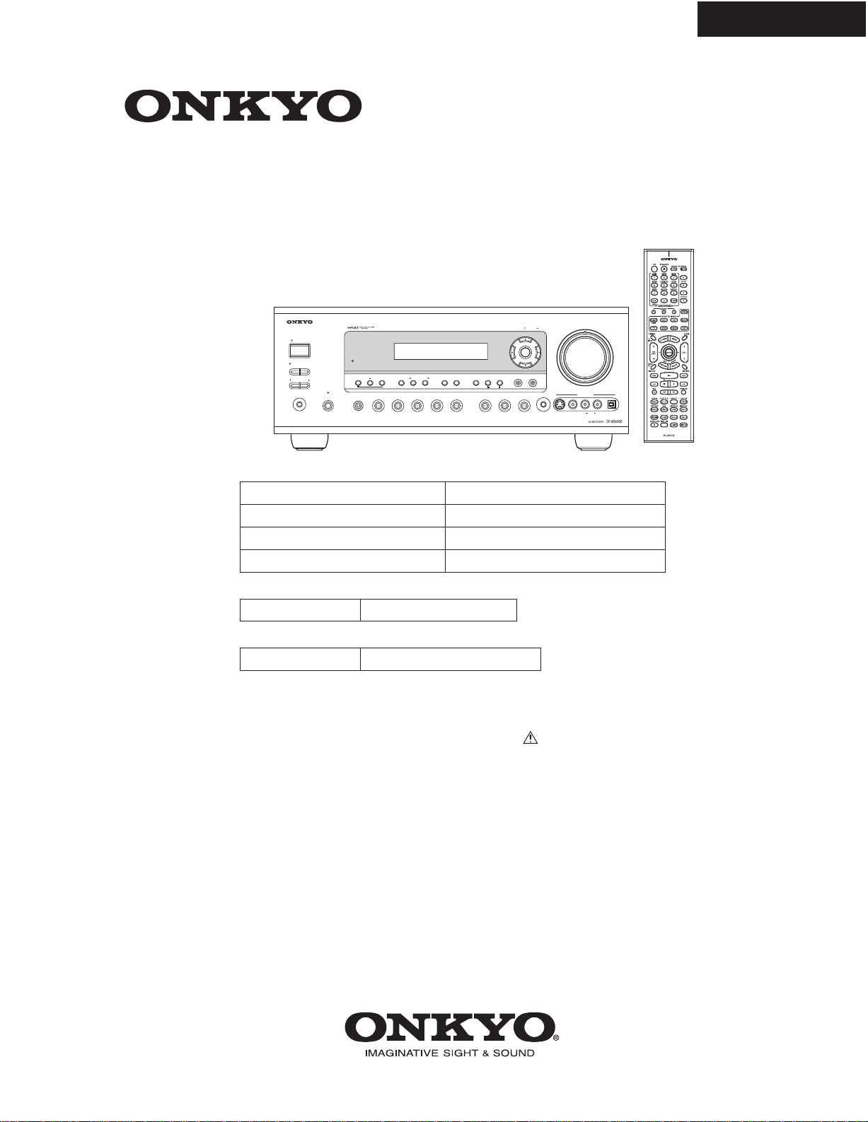
AV RECEIVER
TX-SR603/603E/8360
Ref. No. 3864
042005
MODEL
TX-SR603
MODEL TX-SR603E
MODEL TX-SR8360
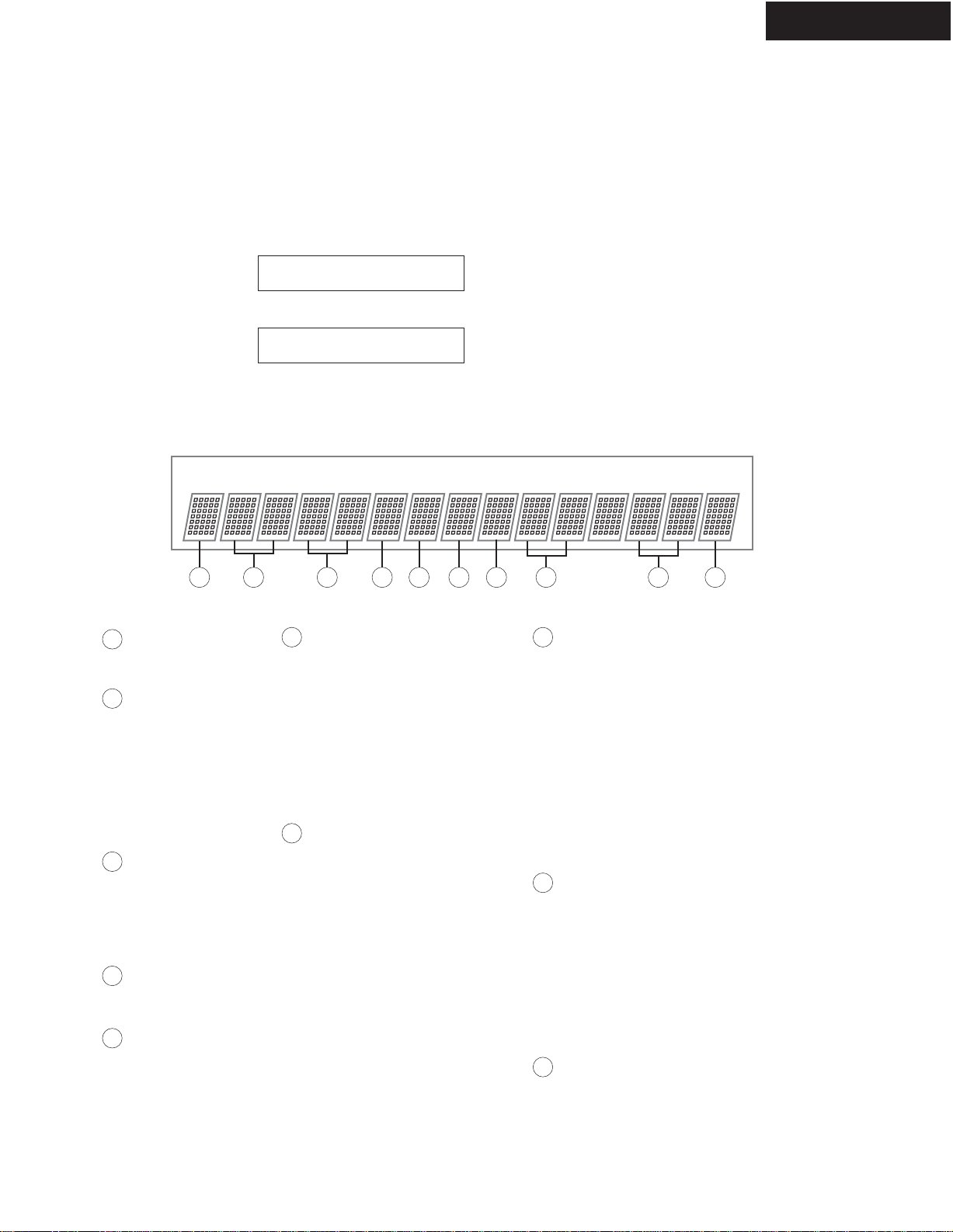
CLEAR
TUNING MODE
TUNING / PRESET
ENTER
RETURN
SETUP
STANDBY/ON
STANDBY
OFF
ZONE2
ZONE 2 LEVEL
PHONES
PURE AUDIO MULTl CH
TONE
+
STEREO
DVD VIDEO 1 VIDEO 2
VCR 1 VCR 2
LISTENING MODE
DISPLAY
DIGITAL INPUT
RT/PTY/TP MEMORY
VIDEO 3 VIDEO 4 TAPE TUNER CD
TX-SR603 Black, Golden and Silver models
B MDD, B MDC, S MDC
B MPA, S MPA
B MWT, G MWT
G MGR, G MGQ, G MGK
TX-SR603E
Black and Silver models
120V AC, 60Hz
230-240V AC, 50Hz
120V/220-230V AC, 50/60Hz
220-230V AC, 50/60Hz
230-240V AC, 50HzB MPP, S MPP
SETUP MIC S VIDEO VIDEO
MASTER VOLUME
VIDEO 4 INPUT
LR
AUDIO
DIGITAL
RC-591M
TX-SR8360
SAFETY-RELATED COMPONENT
WARNING!!
COMPONENTS IDENTIFIED BY MARK ON THE
SCHEMATIC DIAGRAM AND IN THE PARTS LIST ARE
CRITICAL FOR RISK OF FIRE AND ELECTRIC SHOCK.
REPLACE THESE COMPONENTS WITH ONKYO
PARTS WHOSE PART NUMBERS APPEAR AS SHOWN
IN THIS MANUAL.
MAKE LEAKAGE-CURRENT OR RESISTANCE
MEASUREMENTS TO DETERMINE THAT EXPOSED
PARTS ARE ACCEPTABLY INSULATED FROM THE
SUPPLY CIRCUIT BEFORE RETURNING THE
APPLIANCE TO THE CUSTOMER.
Golden model
220-230V AC, 50/60HzG MGR
SPECIFICATIONS
TX-SR603/603E/8360
Amplifier Section
Power Output
2 channel driven: North American: 85 W + 85 W
(8 , 20Hz-20kHz, FTC)
European: 120 W + 120 W
(6 , 1kHz, DIN)
Asian, Australian: 150 W + 150 W
(6 , 1kHz, JEITA)
Dynamic Power 220 W + 220 W (3 , Front)
165 W + 165 W (4 , Front)
100 W + 100 W (8 , Front)
THD
(Total Harmonic Distortion) 0.08 % (Power Rated)
Damping Factor 60 (Front, 1kHz, 8 )
Input Sensitivity and Impedance 200 mV/ 47 k (LINE)
Output Level and Impedance 200 mV/ 470 (REC OUT)
Frequency Response 10 Hz-100 kHz/ +1 dB-3 dB (Direct
mode)
Tone Control 10 dB, 50 Hz (BASS)
10 dB, 10 kHz (TREBLE)
SN Ratio 106 dB (LINE IHF-A)
Speaker Impedance North American: 6 Others: 4 -
Video Section
Input Sensitivity/Output Level
and Impedance 1 Vp-p /75 (Component and S-Video Y)
0.7 Vp-p /75 (Component Pb/Cb,Pr/Cr)
0.28 Vp-p /75 (S-Video C)
1 Vp-p /75 (Composite)
Component Video
Frequency Response 5 Hz-50 MHz
Tuner Section
FM
Tuning Frequency Range North American: 87.5 MHz-107.9 MHz
Others: 87.5 MHz- 108.0 MHz
Usable Sensitivity Stereo: 17.2 dBf 2 V(75 IHF)
Mono: 11.2 dBf 1 V(75 IHF)
S/N Ratio Stereo: 70 dB (IHF-A)
Mono: 76 dB (IHF-A)
THD Stereo: 0.3 % (1kHz)
Mono: 0.2 % (1kHz)
Frequency Response 30 Hz-15 kHz / 1 dB
Stereo Separation 45 dB (1kHz)
AM
Tuning Frequency Range North American: 530 kHz-1700 kHz
Others: 522 kHz-1611 kHz
Usable Sensitivity 30 V
S/N Ratio 40 dB
THD 0.70%
General
Power Supply North American: AC 120 V, 60 Hz
Australian and European:
AC 230-240 V, 50 Hz
Others: AC 120/220-230 V, 50/60 Hz
AC 230-240 V, 50Hz
AC 220-230 V, 50/60 Hz
Power Consumption North American: 6.7A
Others: 650 W
Stand-by Power Consumption 1.0 W
Dimensions
(W x H x D) 435 W x 175 H x 430 D mm
17-1/8" W x 6-7/8" H x 16-15/16" D inches
Weight North American, Australian,
European, Singapore
and East southern asian: 13.6 kg
30.0 lbs
Others: 14.8 kg
32.6 lbs
Video Inputs
Component Video Input 1, 2, 3
S-Video Compatible Jack Input DVD, VIDEO1, VIDEO2, VIDEO3, VIDEO4
A/V Input DVD, VIDEO1, VIDEO2, VIDEO3, VIDEO4
Video Outputs
Component Video Output OUT
S-Video Compatible Jack Output MONITOR OUT, VIDEO1, VIDEO2
A/V Output MONITOR OUT, VIDEO1, VIDEO2
Audio Inputs
Digital Inputs Optical: 4(North American)/ 3(other)
Coaxial: 2
Analog Inputs DVD(MULTICHANNEL), VIDEO1,
VIDEO2, VIDEO3, VIDEO4, TAPE, CD
Multichannel Inputs 6
Audio Outputs
Digital Outputs 1(Optical ) 0(Coaxial )
Analog Outputs TAPE, VIDEO1, VIDEO2
Subwoofer Pre Outputs 1
Speaker Outputs 9
Phones 1
Other Jacks
IR Input 1
12V Trigger Out 1
Specifications and features are subject to change without notice.

SERVICE PROCEDURE
1. Replacing the fuses
This symbol located near the fuse indicates that the
fuse used is show operating type, For continued protection against
fire hazard, replace with same type fuse, For fuse rating, refer to
the marking adjacent to the symbol.
Ce symbole indique que le fusible utilise est e lent.
Pour une protection permanente, n'utiliser que des fusibles de meme
type. Ce demier est indique la qu le present symbol est apposre.
<Notes>
<DC> : TX-SR603 Canadian model
<DD> : TX-SR603 American model
<GK> : TX-SR603 Korean model
<GQ> : TX-SR603 Hong kong model
<GR> : TX-SR603 Chinese model
<PA> : TX-SR603 Australian model
<WT> : TX-SR603 World wide model
<PP> : TX-SR603E European model
<8360> : TX-SR8360 Chinese model
TX-SR603/603E/8360
REF NO.
F901
F901
F901 or
F901 or
F902
F902 or
F902 or
F903
F903 or
F903
F903 or
F903 or
F6901
F6901 or
F6902
F6902 or
F9501
F9501 or
F9501 or
PART NAME
FUSE
FUSE
FUSE
FUSE
FUSE
FUSE
FUSE
FUSE
FUSE
FUSE
FUSE
FUSE
FUSE
FUSE
FUSE
FUSE
FUSE
FUSE
FUSE
DESCRIPTION
10A-UL
5A-SE-EAK
5A-SE-TL250V
5A-SE-TL250V
5A-SE-EAK
5A-SE-TL250V
5A-SE-TL250V
5A-UL/T-237
5A-T/UL-ST2
2.5A-SE-EAK
2.5A-SE-TL250V
2.5A-SE-TL250V
12A-UL/T-314
12A-TUL-250V
12A-UL/T-314
12A-TUL-250V
2.5A-SE-EAK
2.5A-SE-TL250V
2.5A-T/UL-ST2
PART NO.
252199
252078
252244
252278
252078
252244
252278
252164
252258
252075
252241
252275
252196
252301
252196
252301
252075
252241
252254
REMARKS
!, <DD, DC>
!, <WT>
!, <WT>
!, <WT>
!, <PP, PA, WT, GK, GR, GQ>, <8360>
!, <PP, PA, WT, GK, GR, GQ>, <8360>
!, <PP, PA, WT, GK, GR, GQ>
!, <DD, DC>
!, <DD, DC>
!, <PP, PA, WT, GK, GR, GQ>, <8360>
!, <PP, PA, WT, GK, GR, GQ>, <8360>
!, <PP, PA, WT, GK, GR, GQ>, <8360>
!
!
!
!
!
!
!
2. To initialize the unit
1. Press and the hold down the VIDEO 1/VCR button, then press the STANDBY/ON button when the unit is Power on.
2. After " Clear " is displayed, the preset memory and each mode stored in the memory, are initialized and will return to
the factory settings.
3. To check version of microprocessor
Main microprocessor Q701 only.
1. Press and the hold down the DISPLAY button , then press the STANDBY/ON button when the unit is Power on.
Version is displayed on FL display only for 3 seconds.
Ex.
2. Press the STANDBY/ON button to Power off.
Ver.1.01/05305a
4. Memory Backup
The AV receiver uses a battery-less memory backup system in order to retain radio presets and other settings
when it's unplugged or in the case of a power failure.
Although no batteries are required, the AV receiver must be plugged into an AC outlet in order to charge the
backup system. Once it has been charged, the AV receiver will retain the settings for several weeks,
although this depends on the environment and will be shorter in humid climates.
OPERATION CHECK-1
SPEAKER PROTECT-1 (DC VOLTAGE DETECTION)
[When]
1. Exchange power transistors (Q6050 - Q6066).
2. Exchange amplifier PC board ass'y (NAAF-8523).
[Procedure]
<Note>
No load. No input.
1. Press and the hold down the CD button , then press the STANDBY/ON button when the unit is Power ON.
" Test - _ " is displays it only for 5 seconds.
TX-SR603/603E/8360
Test - _
2. Press the VIDEO 3 button, while the character of " Test - _ " is displayed.
Unit will be in the state of " Test-4-00 ".
Blinks
Test - 4-00
3. Repeatedly press TONE
+ button until the character of " Test-4-21 " is displayed.
Test - 4-21
Checking the operation starts automatically as follows.
Test - 4-21
Front L ch
Protect OK
Check
Test - 4-22
Front R ch
Protect OK
Check
Test - 4-23
Center ch
Protect OK
Test - 4-24
Check
Surround L ch
Check
Protect OK
Test - 4-25
Protect OK
Test - 4-26
Protect OK
Test - 4-27
Protect OK
Protect
Surround R ch
Check
Surround Back L ch
Check
Surround Back R ch
Check
If all channel are OK, the character of " Test - 4 - 35 " is displayed.
Test - 4-35
4. Press the STANDBY/ON button.
Turn off
Clear

OPERATION CHECK-2
SPEAKER PROTECT-2 (CURRENT DETECTION)
[When]
1. Exchange power transistors (Q6050 - Q6066).
2. Exchange amplifier PC board ass'y (NAAF-8523).
[Procedure]
<Note>
No input.
Do not check two or more channels at the same time.
Do not connect dummy load to speaker terminals fro seconds 2 or more.
1. Press and the hold down the CD button , then press the STANDBY/ON button when the unit is Power ON.
" Test - _ " is displays it only for 5 seconds.
TX-SR603/603E/8360
Test - _
2. Press the VIDEO 3 button, while the character of " Test - _ " is displayed.
Unit will be in the state of " Test-4-00 ".
Blinks
Test - 4-00
3. Repeatedly press TONE
+ button until the character of " Test-4-35 " is displayed.
Test - 4-35
4. Connect the Dummy load of 3 ohms to the Front Lch speakers terminal.
At this time, check the speaker relay is not turned off.
Test - 4-35
5. Connect the dummy load of 1 ohm to the Front Lch speakers terminal.
At that time, you check the speaker relay is turned off and " Protect " is displayed.
Protect
Disconnect the dummy load at once when check the display of " Protect ".
Test - 4-35
6. Check other channels according to the same procedure.
7. Press the STANDBY/ON button.
Clear
Turn off
OPERATION CHECK-3
CONTROL OF POWER SUPPLY (OUTPUT SENSOR AND THERMAL SENSOR)
[When]
1. Exchange power transistors (Q6050 - Q6066).
2. Exchange power amplifier PC board ass'y (NAAF-8523).
3. Exchange thermal sensor PC board ass'y (NAETC-8526).
[Procedure]
<Note>
No output. No input.
Output sensor
1. Press and the hold down the CD button , then press the STANDBY/ON button when the unit is Power ON.
" Test - _ " is displays it only for 5 seconds.
TX-SR603/603E/8360
Test - _
2. Press the VIDEO 3 button, while the character of " Test - _ " is displayed.
Unit will be in the state of " Test-4-00 ".
Blinks
Test - 4-00
3. Repeatedly press TONE
+ button until the character of " Test-4-37 " is displayed.
Test - 4-37
4. Adjusts MASTER VOLUME to Max. position.
At this time, check the character of " FM STEREO " displayed.
And, check relay RL6901 and RL6902 are turned off in 2 - 3 seconds.
FM STEREO
Test - 4-37
5. Press the STANDBY/ON button.
Turn off
Clear
Thermal sensor
1. Press and hold down the DISPLAY button, then press the STANDBY button when the unit is power ON.
" Ver. 0.50/05131a " is displays it only for 2 seconds.
<Ex.>
Ver. 0.50/05131a
2. Press the TONE button, while the character of " Ver.0.50/05131a " is displayed.
<Ex.>
3. Check the displayed temperature is +/-20 C of the ambient temperatures.
4. Press STANDBY/ON button.
T: 25 C/ 77 F
Turn off
Clear
OPERATION CHECK-4
DSP DEBUG MODE
Check the operation of the circuit around DSP by the display in this mode.
This information helps to pursue the faulty point.
To set in DSP debug mode
1. Press and hold down the DISPLAY button, then press the STANDBY button when the unit is power ON.
" Ver. 0.50/05131a " is displays it only for 2 seconds.
<Ex.>
Ver. 0.50/05131a
2. Press the DISPLAY button, while the character of " Ver.0.50/05131a " is displayed.
E1A48K015FF 23o
To exit
Press STANDBY/ON button.
Content of display
TX-SR603/603E/8360
1 42 5 6 87 103 9
--------- DIR --------- ------ MEMORY/DOWNLOAD -----
AUTOBOOT DSP AB CODE
1
UNLOCK
E = UNLOCK
= LOCK
Digital Selecter
2
D = DIGITAL
A = ANALOG
1 = COAX1
2 = OOAX2
3 = OPT1
4 = OPT2
5 = OPT3
7 = FRONT
3
Sampling Frequency
96 = 96kHz
48 = 48kHz
44 = 44kHz
32 = 32kHz
-- = Not detect
Pre Emphasis
4
K = OFF
e = ON
DIR Status
5
0 = ANALOG
1 = PCM
2 = NOT_PCM
3 = DATA
4 = DTSCD
5 = MCH
6 = NOT DECIED
6
0 = FLASH
1 = ab_ac3_pl2
2 = ab_dts_pl2
3 = ab_neo6
4 = sgen_ab
5 = ab_pl2fs
6 = ab_dts_6dol
7 = ab_dts9624
8 = aac_pl2
AUTOBOOT DSP C CODE
7
0 = ac_dts9624
1 = c_neo6
2 = c_oos_no_sd
3 = c_oos
4 = c_oob
5 = c_pl2
6 = c_pl2xthx
7 = c_thx
8 = c_spsetup
9 = version
------------------------- DSP ----------------------------------------
DSP Status
8
00 = Power off
01 = Power on wait
10 = DSP reset
11 = DSP reset wait
12 = DSP AB boot ready
13 = DSP AB boot start
14 = DSP AB boot
15 = DSP C boot ready
16 = DSP C boot start
17 = DSP C boot
18 = DSP soft reset
20 = DSP C app start
DSP Detect Format
9
00 = Null
01 = Dolby Digital
03 = Pause
04 = MPEG1 L1
05 = MPEG1 L23/ MPEG2 w/o
06 = MPEG2 w/e
07 = MPEG2 AAC
08 = MPEG2 L1
09 = MPEG2 L2/3
10
DSP Decode
o = Decode OK
x = Decode NG
-- = Analog in
21 = DSP C HW Config set
22 - 2A = DSP C SW Config set
3F = DSP C kick start
40 = DSP AB App start
41 = DSP AB HW Config set
42 - 4B = DSP AB SW Config set
AF = DSP ab kick start
0B = DTS1
0C = DTS2
0D = DTS3
1B = MPEG2 AAC1
1C = MPEG2 AAC2
20 = Silent
22 = DTS CD
23 = PCM
TX-SR603/603E/8360
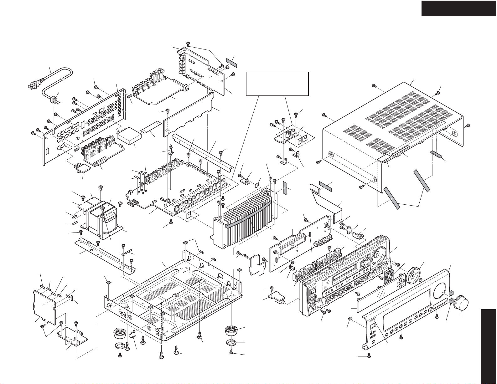
EXPLODED VIEWS-1
P901
F9501C
F902C
F902
A041
A030
x 4 pcs.
U18
F9501
A002
x 4 pcs.
F903c
F903
U20
A022
F901
A068
x 37 pcs.
A093
U19
F6901C
U10
A033
A031
A017
A017
F6901
T901
U24
A014
A002
P101
A018
F6902
U09
A002
x 2 pcs.
U07
A015
U01
A002
x 3 pcs.
A017
A002
x 4 pcs.
U22
A052
A002
x 2 pcs.
A017
U03
A002
Refer to
<Fig-1> in
EXPLODED VIEWS-2
A002
x 4 pcs.
A002
U12
U13
A043
A017
U04
A054
A007
A002
A017
U02
A005
A002
x 4 pcs.
U11
A046
x 2 pcs.
A002
x 3 pcs.
A050
A017
P701
A006
A002
x 2 pcs.
U08
U06
A102
A060
A109
DD, DC Only
A001
A071
A017
A058
A061
x 6 pcs.
A056
A073
U15
A002
x 3 pcs.
U17
F901C
A018
x 4 pcs.
A020
x 3 pcs.
A021
x 2 pcs.
U05
A064
x 4 pcs.
A066
x 8 pcs.
A068
x 4 pcs.
A002
x 6 pcs.
A070
A081
A068
x 3 pcs.
A077
A111
x 2 pcs.
TX-SR603/603E/8360
A110

EXPLODED VIEWS-2
<Fig-1>
TX-SR603/603E/8360
Q6056
Q6066
Q6050A
x 14
A049
x14
Q6055
Q6065
Q6054
Q6064
Q6053
Q6063
Q6052
Q6062
Q6051
Q6061
Q6050
Q6060
TX-SR603/603E/8360
A
BLOCK DIAGRAM
1
2
3
SETUP MIC
VIDEO4
INPUT
TAPE OUT
TAPE IN
VIDEO3 IN
VIDEO2 OUT
VIDEO2 IN
VIDEO1 OUT
VIDEO1 IN
FRONT
SURROUND
DVD
CENTER
(MULTI INPUT)
SUBWOOFER
CD
L
R
L
R
MIC AMP
BCDEFGH
TUNER UNIT
51
52
53
54
55
56
57
58
59
60
61
62
63
64
65
66
67
68
69
70
71
73
73
74
NJW1157
41
43
27
Z2_L
29
28
Z2_R
30
RECOUT_L
21
23
25
RECOUT_R
22
24
26
SOURCE_L
SOURCE_R
V1_OUT_L
V1_OUT_R
TAPE_OUT_R
TAPE_OUT_L
+
+
V2_OUT_L
V2_OUT_R
12
17
11
18
10
19
20
21
9
8
42
44
-6dB
NJU7311
46
45
48
47
4
25
3
26
MIX_L
2
MIX_R
27
+9.7dB
INVERT
-6dB
VOLIN_SBL
7
VOLIN_SBR
22
5
24
6
23
ADLT+
ADRT+
ADLT-
ADRT-
MCH_SW
DAC_CT
DAC_SW
DAC_SL
DAC_SR
DAC_SBR
DAC_SBL
MCH_CT
DAC_FL
DAC_FR
MCH_SR
MCH_SL
80
88
81
89
82
90
87
95
83
91
84
92
85
93
86
94
4
+6dB
DIGITAL
COAXIAL
IN1
IN2
IN 4
IN 1
5
OPTICAL
IN 2
ADLT+
ADLT-
RX0
RX1
RX6
RX2
RX3
RX4
TX
ADRT-
ADRT+
16
15
14
13
49
48
43
47
46
45
44
42
50
2ch ADC
DIR
VLSCLPF
37
36
IN 3
CS42518
OUT
VLSCLPF
+6dB
LPF
35
34
32
33
LPF
LPF
31
30
28
29
8ch DAC

A
A
VOLUME
TONE
TONE
1
2
3
+20.2dB
8
4
FL_PO
FR_PO
CT_PO
SW_PO
SL_PO
POWER
AMPLIFIER
+29dB
+29dB
+29dB
+29dB
+29dB
TX-SR603TX-SR603
PHONES
SPEAKERS
L
FRONT
R
CENTER
L
SURROUND
R
LPF
SR_PO
5
SBL_PO
6
SBR_PO
7
PREOUT
SUBWOOFER
+29dB
+29dB
L
SURROUND
BACK
R
L
ZONE2
R
ZONE2 LINEOUT
Z2L_PO
Z2R_PO
Z2LMUT
AMUT
SBMUT
4M Bit
FLASH ROM
MX29LV040
LPF
26
27
22
LPF
23
21
20
110
62
109
63
107
64
106
1
118
58
86
54
134
81
80
DSP
CS494003
L
R
2M Byte
SD_RAM
IC42S16100
DE-MODULATOR
To Microprocessor
Z2RL
SBRL
SPRLCS
HPIN
SPRLF
12V TRIGGER
CONTROL
IR
RI
INTERFACE
12V TRIGGER OUT
ZONE 2
IR IN
RI
TX-SR603/603E/8360 TX-SR603/603E/8360
A
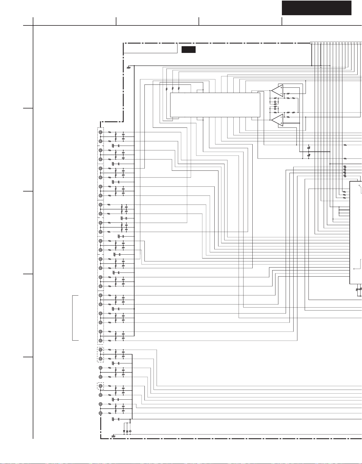
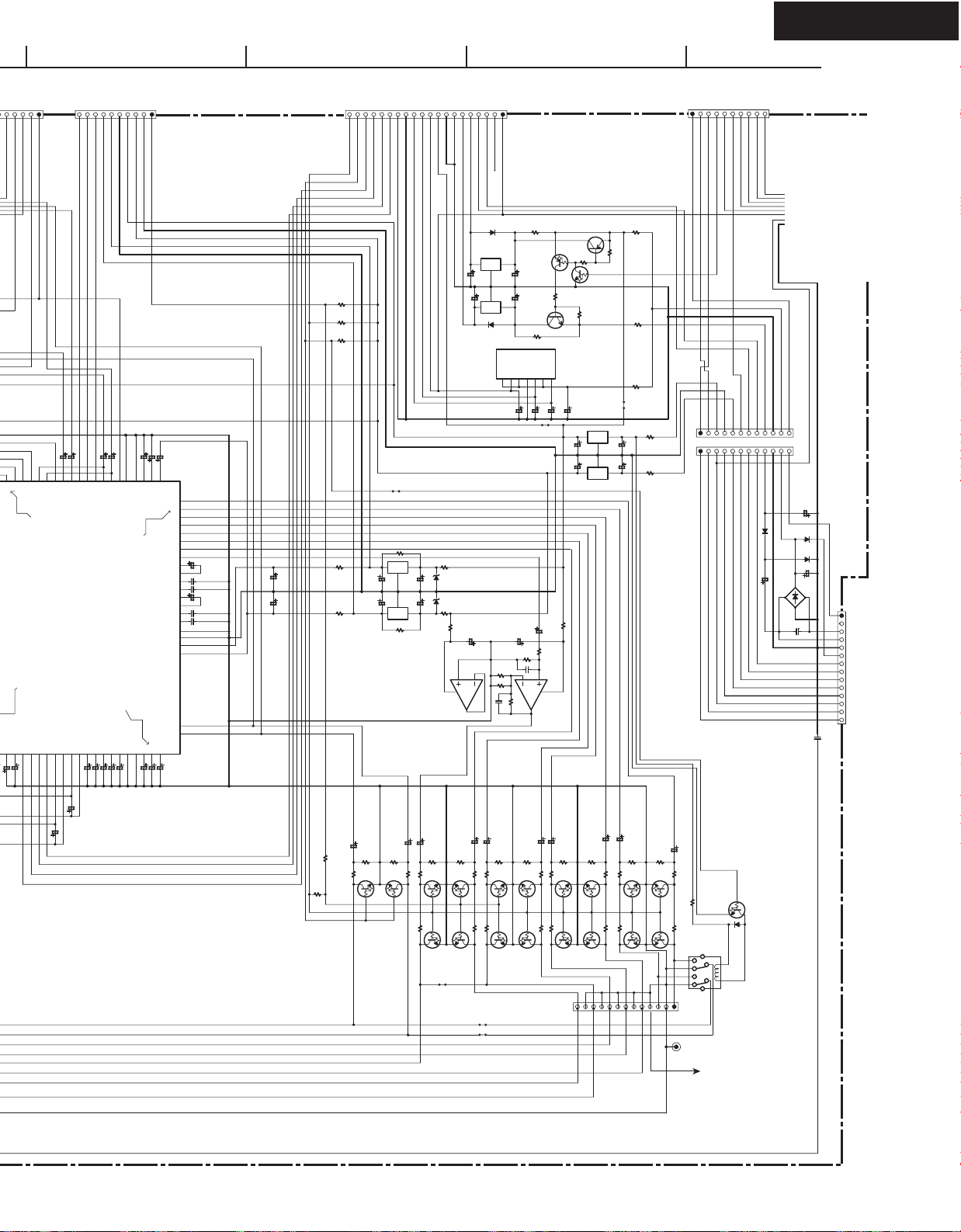
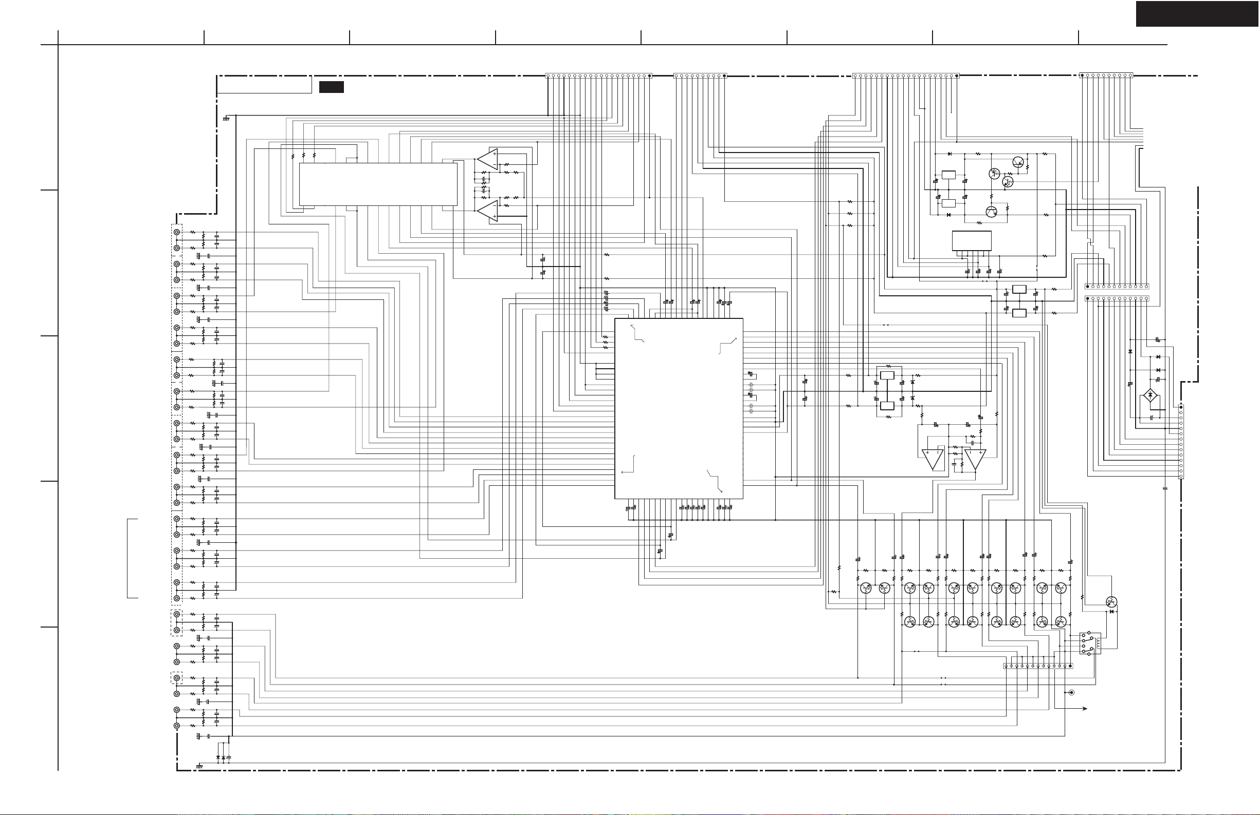
SCHEMATIC DIAGRAMS-1
AUDIO INPUT SECTION
1
P7901
NC
R5501
NC
R5502
R5542
NC
P7902
2
TAPE OUT
TAPE IN
VIDEO3 IN
VIDEO2 OUT
3
VIDEO2 IN
VIDEO1 OUT
VIDEO1 IN
FRONT R
FRONT L
4
DVD IN
SURR R
SURR L
SUBWOOFER
CENTER
ZONE2
LINEOUT
PREOUT
SUBWOOFER
5
CD
R5503
330
R5504
R5544
330
R5505
R5545
330
R5506
R5546
330
R5507
R5547
330
R5508
R5548
330
R5700
330
R5702
330
P7903
R5705
330
R5707
330
R5513
R5553
330
R5514
R5554
330
P7904
R5515
R5555
330
R5516
R5556
330
R5517
R5557
330
R5518
R5558
330
P7905
R5519
330
R5520
330
R5521
330
R5522
R5562
330
R5523
R5563
330
R5524
330
R5564
P7906
R5525
R
100
R5526
L
P7907
100
R5527
NC
R5528
NC
R5529
100
R5530
NC
R5531
NC
R5532
NC
P6906
NC
R5566
R5567
R5568
R5569
R5570
R5571
R5572
NAAF-8523(1/2)
P5505
A_GND
V1OUT_R
R5541
C5501
NC
NC
C5502
NC
NC
C5701
NC
R5543
C5503
NC
221J
C5504
NC
221J
C5702
103J
C5505
56K
NC
C5506
NC
C5507
221J
C5508
221J
NC
C5513
221J
C5514
221J
C5515
C5516
C5517
221J
C5518
221J
C5519
221J
C5520
221J
C5521
221J
C5522
221J
C5523
221J
C5524
221J
C5525
NC
C5526
NC
C5527
NC
C5528
NC
C5529
102J
C5530
NC
C5531
NC
C5532
NC
NC
NC
D5710
C5509
221J
C5510
221J
C5704
103J
C5511
NC
C5512
NC
PRE_SW/SBL
C5712
TAPEOUT_L
PRE_R
PRE_L
PRE_SR
PRE_SL
PRE_C
PRE_SBR
PRE_SW/SBL
NC
TO_P6906
R5559
R5560
R5561
R5565
56K
56K
R5552
NC
NC
56K
56K
22K
22K
NC
NC
22K
NC
NC
NC
56K
NC
NC
R5549
R5550
R5551
NC
NC
56K
56K
NC
NC
56K
56K
C5703
NC
NC
NC
C5706
103J
C5707
NC
C5708
103J
C5709
103J
C5710
103J
C5711
NC
C5705
D5711
BCDEFGH
TO NADG-8514
U09
C5669
220/25
C5668
220/25
MULTI_SW
MULTI_SR
MULTI_SL
MULTI_C
AIN_R
AIN_L
TUPACK_L
AMPLIFIER PC BOARD
FSWDAT
FSWSTB
FSWCLK
TAPEOUT_R
220
220
220
R5581
R5583
R5582
17181920212223242526272829
CK
NC
DATA
Q5502
NJU7311AM
VSSSTNC
15 16
SOURCE_R
TAPEOUT_R
TUNER_R
TUNER_L
CD_R
CD_L
TAPE_R
TAPE_L
VIDEO3_R
VIDEO3_L
V2OUT_R
V2OUT_L
VIDEO2_R VIDEO2_R
VIDEO2_L VIDEO2_L
V1OUT_L
VIDEO1_R
VIDEO1_L
MULTI_R
MULTI_L
MULTI_SR
MULTI_SL
MULTI_SW
MULTI_C
R_COM4
L_COM4
12
13
14
R7
L7
11
R_COM3
L_COM3
10
SOURCE_L
R6
L6
9
V1OUT_R
R5
L5
8
V1OUT_L
R_COM2
L_COM2
7
DAC_SBR
R4
L4
6
DAC_SBL
Z2_R
R3
L3
5
Z2_L
R_COM
L_COM
4
DMIXR
DAC_FR
R1
R2
L2L1VEE
2
3
DMIXL
DAC_FL
30
VDD
1
330J
330J
7
10K
R5590
C5590
C5591
R5598
10K
1
4
Q5503
Q5503
8
10K
R5594
10K
R5595
5
6
R5592
2
3
10K
R5591
1.2K
470
R5593
1.2K
470
R5596
R5597
R5599
10K
NJM4565M-D
TUPACK_R
VIDEO4_L
MIC
VLTNDAT
VLTNCLK
VLTNSTB
VIDEO4_R
R5666
VLTNDAT
VLTNCLK
VLTNSTB
R5589
R5588
R5587
MIC
MIC
VIDEO4_R
VIDEO4_L
TUPACK_R
TUPACK_L
TUNER_R
TUNER_L
CD_R
CD_L
TAPE_R
TAPE_L
VIDEO3_R
VIDEO3_L
VIDEO1_R
VIDEO1_L
MULTI_R Z2_L
MULTI_L Z2_R
AIN_L
AIN_R
FSWSTB
22
R5667
22
C5571
C5569 10/50
C5570 10/50
C5568 10/50
220
220
220
DAC_FL
FSWCLK
FSWDAT
DAC_SBR
10/50
81
82
LAIN
80
LATCH
79
CLOCK
78
DAT
77
DGND
76
NC
75
R12IN
74
L12IN
73
R11IN
72
L11IN
71
R10IN
70
L10IN
69
R9IN
68
L9IN
67
R8IN
66
L8IN
65
R7IN
64
L7IN
63
R6IN
62
L6IN
61
R5IN
60
L5IN
59
R4IN
58
L4IN
57
R3IN
56
L3IN
55
54
53
52
51
VSSOUT
VDDOUT
49
50
10/50
10/50
C5567
C5566
SOURCE_L
SOURCE_R
<Note>
NC=No mount of parts.
TO NADG-8514
P303
+7V
DAC_FL
DAC_FR
DAC_SW
RSAIN
CAIN
FR+
ADLT-
LBAIN
FL-
RBAIN
FL+
ADLT+
10/50
10/50
C5573
C5572
LBIN
RBIN
SWAIN
Q5501
NJW1157B
DCR_IN
DCL_IN
DCR_OUT
AIN_L
AIN_R
C5564
10/50
C5565
DAC_CT
10/50
DAC_SBL
DAC_SBR
10/50
81828384858687888990919293949596979899
LAIN
LSAIN
RAIN
R2IN
L2IN
R1IN
L1IN
FR-
VSSOUT
VDDOUT
50
10/50
ADRT-
ADRT+
C5566
<Note>
NC=No mount of parts.
DAC_SL
DAC_SR
CBIN
LSBIN
DCL_OUT
DCCAP_SW
47/25
C5563
-7V
10/50
10/50
C5574
C5575
LBBIN
RBBIN
RSBIN
DCCAP_RB
DCCAP_LB
DCCAP_RS
47/25
47/25
C5560
C5562 47/25
C5561
+12VA
GND
SWBIN
LOUT
ROUT
COUT
DCCAP_C
DCCAP_R
DCCAP_LS
GND
47/25
C5559
-12VA
10/50
C5576
GND
VSSOUT2
FIL_BL
FIL_TL
FIL_BR
FIL_TR
REC_A1L
REC_A1R
REC_A2L
REC_A2R
REC_A3L
REC_A3R
DCCAP_L
REC_A4L
REC_A4R
REC_A1L
REC_A1R
GND
C5558 47/25
P301
SB/PREMUTE
1/100
10/50
C5577
C5578
100
1
2
TCCAP
3
VDDOUT2
4
LSOUT
5
RSOUT
6
LBOUT
7
RBOUT
8
SWOUT
9
DC_L1
10
DC_L2
11
12
DC_R1
13
DC_R2
14
15
16
GND
17
GND
18
V+
19
V-
20
21
22
23
24
25
26
27
28
29
30
31323334353637383940414243444546474849
47/25
C5557
C5556 47/25
FL_OUT
FR_OUT
CT_OUT
SL_OUT
SR_OUT
SBL_OUT
SBR_OUT
SW_OUT
C5555
224J
472J
C5554
224J
C5550
4.7/50
C5553
4.7/50
472J
C5551
C5552
C5673
C5674
220/25
220/25
P302
SB/PREMUTE
R5813
NC
R5814
AMUT
Z2MUT
R5680
100K
R5681
100K
R5682
100K
R5671
22
R5672
22
0
TO NADG-8514
AMUT
Z2MUT
ADRT-
ADRT+
ADLT-
R5808
C5671
10/50
C5672
10/50
Q5672
79L07
Z2_R
47/50
C5609
R5608
R5609
220K
2.2K
R5619
RN1441
Q5609
ADLT+
J5620
O
O
R5809
220K
G
G
C5608
I
I
47/50
2.2K
NC
NC
Z2_L
Q5608
2.5VDSP
RN1441
3.3VDSP
Q5671
R5665
10/50
R5664
10/50
C5666 C5667
SW
C5607
10/50
R5607
220K
270
R5618
R5617
Q5607
100
R5627
Q5617
RN1441
J5654
NC
PRE_SW/SBL
78L07
D5671
NC
D5672
NC
22
R5663
RN1441
22
4
R5606
220K
5
10S
-5V_VIDEO
+5V_VIDEO
LM2940CT-5.0
C5652
220/25
10/50
C5653
D5651
C5643
22/50
22
C5665
220/25
6
Q5630
7
SBR_OUT
47/50
C5606
2.2K
R5616
Q5606
0
R5626
NC
Q5616
J5659
J5658
POFF
D5650
Q5654
O
G
G
79M05FA
SBL_OUT
R5605
RN1441
NC
NC
MPU_GND
Q5655
C5642
22/50
R5632
15K
R5633
1.2K
220K
R5615
0
5V
TO POWER AMP
R5811
Q5652
RN2402
I
10/50
C5650
10/50
C5651
IO
R5812
5.0V2
GND4
MODE1
VCC
3
C5664
C5630
220/25
R5631
47K
2
103J
R5634
10K
C5632
SW
47/50
C5605
C5604
R5604
220K
2.2K
Q5605
RN1441
Q5604
NC
NC
R5625
Q5614
Q5615
NC
Q5653
2SD1468-SR
NC
PURE AUDIO SWITCH
Q5640
AN34060A
2.5V7
3.3V5
NC6
J5620
22
10/16
220
R5630
C5631
221J
3
8
1
Q5630
NJM4565M
SL_OUT
SR_OUT
47/50
R5603
220K
2.2K
R5614
R5613
Q5603
RN1441
0
R5624
R5623
PRE_SR
PRE_SL
PRE_C
PRE_SBR
PRE_SW/SBL
2SB1068-K
Q5650
R5653
1K
Q5651
RN1402
KRC102S
18K
R5655
47K
R5656
C5640
C5641
22/50
22/50
Q5660 78M12HF
IO
G
10/50
C5662
G
10/50
C5663
IO
79M12HF
Q5661
R5662
CT_OUT
47/50
C5602
C5603
47/50
R5602
220K
2.2K
2.2K
R5612
Q5602
RN1441
RN1441
0
0
NC
NC
R5622
Q5612
Q5613
R5650
47K
R5652
VPOWER
C5660
C5661
FR_OUT
R5601
220K
2.2K
R5611
RN1441
Q5601
0
R5621
0.22
R5651
0.22
R5640
0.22
J5644
10/50
10/50
C5601
47/50
NC
R5660
12
R5661
22
Q5611
+12V
-12V
R5600
220K
Q5610
FL_OUT
47/50
C5600
R5610
Q5600
NC
TO NADG-8514
2.2K
RN1441
0
R5620
P5504
PRE_R
PRE_L
P5503
-VP
JL5501B
JL5501A
NC
R5668
RL5700
FLAC2
FLAC1
FLAC1
FLAC2
HPDET
VPOWER
A_GND
+24V
A1_GND
NC
SEC1H
APOWER
APOWER
-24V
APOWER
VOLH
POFF
POFF
Q5700
D5700
NC
NAAF-8540
P311B
PRO
THRM
TO NAAF-8523
(2/2)
-VP
-12V
DGND
+12V
10S
10S
-12V
+12V
-VP
MPUGND
RN1N4003
D9020
C9020
1000/16
D9005
C9005
334J MMT
NC
+24V
10/50
C9021
D3SBA20
C9017
102J
D9011
RN1N4003
D9021
RN1N4003
C9010
4700/16
+12VD
P9502
TO NAPS-8535
TX-SR603/603E/8360
A
SCHEMATIC DIAGRAMS-1
AUDIO INPUT SECTION
1
P7901
NC
R5501
NC
R5502
R5542
NC
P7902
2
TAPE OUT
TAPE IN
VIDEO3 IN
VIDEO2 OUT
3
VIDEO2 IN
VIDEO1 OUT
VIDEO1 IN
FRONT R
FRONT L
4
DVD IN
SURR R
SURR L
SUBWOOFER
CENTER
ZONE2
LINEOUT
PREOUT
SUBWOOFER
5
CD
R5503
330
R5504
R5544
330
R5505
R5545
330
R5506
R5546
330
R5507
R5547
330
R5508
R5548
330
R5700
330
R5702
330
P7903
R5705
330
R5707
330
R5513
R5553
330
R5514
R5554
330
P7904
R5515
R5555
330
R5516
R5556
330
R5517
R5557
330
R5518
R5558
330
P7905
R5519
330
R5520
330
R5521
330
R5522
R5562
330
R5523
R5563
330
R5524
330
R5564
P7906
R5525
R
100
R5526
L
P7907
100
R5527
NC
R5528
NC
R5529
100
R5530
NC
R5531
NC
R5532
NC
P6906
NC
R5566
R5567
R5568
R5569
R5570
R5571
R5572
NAAF-8523(1/2)
P5505
A_GND
V1OUT_R
R5541
C5501
NC
NC
C5502
NC
NC
C5701
NC
R5543
C5503
NC
221J
C5504
NC
221J
C5702
103J
C5505
56K
NC
C5506
NC
C5507
221J
C5508
221J
NC
C5513
221J
C5514
221J
C5515
C5516
C5517
221J
C5518
221J
C5519
221J
C5520
221J
C5521
221J
C5522
221J
C5523
221J
C5524
221J
C5525
NC
C5526
NC
C5527
NC
C5528
NC
C5529
102J
C5530
NC
C5531
NC
C5532
NC
NC
NC
D5710
C5509
221J
C5510
221J
C5704
103J
C5511
NC
C5512
NC
PRE_SW/SBL
C5712
TAPEOUT_L
PRE_R
PRE_L
PRE_SR
PRE_SL
PRE_C
PRE_SBR
PRE_SW/SBL
NC
TO_P6906
R5559
R5560
R5561
R5565
56K
56K
R5552
NC
NC
56K
56K
22K
22K
NC
NC
22K
NC
NC
NC
56K
NC
NC
R5549
R5550
R5551
NC
NC
56K
56K
NC
NC
56K
56K
C5703
NC
NC
NC
C5706
103J
C5707
NC
C5708
103J
C5709
103J
C5710
103J
C5711
NC
C5705
D5711
BCDEFGH
DAC_SBL
LSAIN
RSAIN
RAIN
FR-
FR+
ADRT+
P303
DAC_SW
LBAIN
CAIN
FL-
ADLT-
ADLT+
RBAIN
FL+
AIN_R
TO NADG-8514
+7V
DAC_CT
DAC_SL
DAC_SR
-7V
10/50
10/50
C5573
RBIN
Q5501
DCL_IN
AIN_L
10/50
C5564
10/50
CBIN
LSBIN
RSBIN
DCL_OUT
DCCAP_SW
DCCAP_RB
47/25
C5563
C5562 47/25
10/50
C5574
C5575
LBBIN
RBBIN
DCCAP_LB
DCCAP_RS
47/25
47/25
C5560
C5561
10/50
C5572
LBIN
SWAIN
NJW1157B
DCR_IN
DCR_OUT
C5565
+12VA
-12VA
GND
GND
SWBIN
LOUT
ROUT
COUT
DCCAP_C
DCCAP_R
DCCAP_L
DCCAP_LS
GND
GND
47/25
C5559
SB/PREMUTE
1/100
10/50
10/50
C5576
C5577
C5578
100
TCCAP
VSSOUT2
VDDOUT2
LSOUT
RSOUT
LBOUT
RBOUT
SWOUT
DC_L1
DC_L2
FIL_BL
FIL_TL
DC_R1
DC_R2
FIL_BR
FIL_TR
GND
GND
V+
VREC_A1L
REC_A1R
REC_A2L
REC_A2R
REC_A3L
REC_A3R
REC_A4L
REC_A4R
REC_A1L
REC_A1R
31323334353637383940414243444546474849
47/25
C5558 47/25
C5557
C5556 47/25
P301
10
11
12
13
14
15
16
17
18
19
20
21
22
23
24
25
26
27
28
29
30
1
2
3
4
5
6
7
8
9
FL_OUT
FR_OUT
CT_OUT
SL_OUT
SR_OUT
SBL_OUT
SBR_OUT
SW_OUT
C5555
224J
472J
C5554
224J
C5550
4.7/50
C5553
4.7/50
472J
C5551
C5552
C5673
C5674
220/25
220/25
P302
SB/PREMUTE
R5813
NC
R5814
AMUT
Z2MUT
R5680
100K
R5681
100K
R5682
100K
R5671
22
R5672
22
0
TO NADG-8514
AMUT
Z2MUT
ADRT-
ADRT+
ADLT-
R5808
C5671
10/50
C5672
10/50
Q5672
79L07
Z2_R
47/50
C5609
R5608
R5609
220K
2.2K
R5619
RN1441
Q5609
ADLT+
J5620
O
O
R5809
220K
G
G
C5608
I
I
47/50
2.2K
2.5VDSP
NC
NC
Z2_L
RN1441
Q5608
C5666 C5667
R5618
3.3VDSP
Q5671
R5665
10/50
R5664
10/50
R5663
SW
C5607
10/50
R5607
220K
270
R5617
Q5607
100
R5627
Q5617
RN1441
J5654
NC
PRE_SW/SBL
78L07
22
D5671
NC
D5672
NC
22
R5606
220K
RN1441
-5V_VIDEO
+5V_VIDEO
C5652
220/25
10/50
C5653
D5651
22
C5665
220/25
5
4
Q5630
7
C5606
2.2K
R5626
NC
Q5616
10S
POFF
MPU_GND
D5650
Q5654
LM2940CT-5.0
O
I
G
G
IO
79M05FA
Q5655
C5643
C5642
22/50
22/50
C5664
220/25
R5632
15K
6
R5633
1.2K
C5632
SBR_OUT
SBL_OUT
47/50
47/50
R5605
220K
2.2K
R5615
R5616
RN1441
Q5606
0
0
R5625
NC
J5659
NC
J5658
5V
TO POWER AMP
R5811
NC
Q5652
RN2402
10/50
C5650
10/50
C5651
Q5653
R5812
NC
3.3V5
5.0V2
GND4
MODE1
VCC
3
J5620
10/16
C5630
R5631
47K
2
103J
R5634
1
10K
SW
C5605
C5604
47/50
R5604
220K
2.2K
R5614
Q5605
RN1441
Q5604
NC
NC
R5624
Q5614
Q5615
PRE_SBR
PRE_SW/SBL
2SB1068-K
Q5650
R5653
1K
18K
R5655
2SD1468-SR
PURE AUDIO SWITCH
Q5640
AN34060A
2.5V7
NC6
Q5660 78M12HF
C5662
C5663
Q5661
22
R5662
220
R5630
C5631
221J
3
8
Q5630
NJM4565M
SL_OUT
SR_OUT
C5603
47/50
R5603
220K
2.2K
R5613
RN1441
Q5603
RN1441
0
0
NC
R5623
Q5613
PRE_SR
PRE_SL
PRE_C
R5656
C5641
22/50
10/50
10/50
R5602
220K
RN1441
Q5612
Q5651
RN1402
KRC102S
47K
C5640
22/50
IO
G
G
IO
79M12HF
CT_OUT
47/50
C5602
2.2K
R5612
Q5602
0
NC
R5622
R5650
47K
R5652
VPOWER
C5660
C5661
FR_OUT
R5601
220K
2.2K
R5611
RN1441
Q5601
0
R5621
0.22
R5651
0.22
R5640
0.22
J5644
10/50
10/50
C5601
47/50
NC
R5660
12
R5661
22
R5600
Q5611
+12V
-12V
220K
Q5610
NC
TO NADG-8514
-VP
FLAC2
FLAC1
HPDET
VPOWER
A_GND
JL5501B
JL5501A
FLAC2
FLAC1
+24V
A1_GND
FL_OUT
47/50
C5600
2.2K
R5610
NC
Q5600
RN1441
0
R5668
R5620
NC
RL5700
P5504
PRE_R
PRE_L
P5503
NAAF-8540
SEC1H
APOWER
APOWER
-24V
APOWER
VOLH
POFF
POFF
Q5700
D5700
NC
THRM
10S
10S
NC
P311B
PRO
-12V
DGND
-12V
MPUGND
RN1N4003
D9020
C9020
1000/16
TO NAAF-8523
(2/2)
-VP
+12V
+24V
+12V
-VP
10/50
C9021
D9011
RN1N4003
D9021
RN1N4003
C9010
4700/16
+12VD
P9502
D9005
D3SBA20
C9005
334J MMT
C9017
102J
TO NAPS-8535
TO NADG-8514
U09
TUPACK_L
TUPACK_R
VIDEO4_L
AMPLIFIER PC BOARD
FSWDAT
FSWSTB
FSWCLK
TAPEOUT_R
220
220
220
R5581
R5583
R5582
17181920212223242526272829
CK
NC
DATA
Q5502
NJU7311AM
VSSSTNC
15 16
SOURCE_R
TAPEOUT_R
TUNER_R
TUNER_L
CD_R
CD_L
TAPE_R
TAPE_L
VIDEO3_R
VIDEO3_L
V2OUT_R
V2OUT_L
VIDEO2_R VIDEO2_R
VIDEO2_L VIDEO2_L
V1OUT_L
VIDEO1_R
VIDEO1_L
MULTI_R
MULTI_L
MULTI_SR
MULTI_SL
MULTI_SW
MULTI_C
R_COM4
L_COM4
12
13
14
R7
L7
11
R_COM3
L_COM3
10
SOURCE_L
R6
L6
9
V1OUT_R
V1OUT_L
Z2_R
DAC_SBR
R5
L5
8
R_COM2
L_COM2
7
R4
L4
6
Z2_L
DAC_SBL
R3
L3
5
R_COM
L_COM
4
DMIXR
DAC_FR
R1
R2
L2L1VEE
2
3
DMIXL
DAC_FL
30
VDD
1
330J
330J
7
10K
R5590
C5590
C5591
R5598
10K
1
4
Q5503
Q5503
8
10K
R5594
10K
R5595
5
6
R5592
2
3
10K
R5591
1.2K
470
R5593
1.2K
470
R5596
R5597
R5599
10K
NJM4565M-D
C5669
220/25
C5668
220/25
MULTI_SW
MULTI_SR
MULTI_SL
MULTI_C
AIN_R
AIN_L
VIDEO4_R
MIC
VLTNDAT
VLTNCLK
VLTNSTB
R5666
VLTNDAT
VLTNCLK
VLTNSTB
R5589
R5588
R5587
MIC
MIC
VIDEO4_R
VIDEO4_L
TUPACK_R
TUPACK_L
TUNER_R
TUNER_L
CD_R
CD_L
TAPE_R
TAPE_L
VIDEO3_R
VIDEO3_L
VIDEO1_R
VIDEO1_L
MULTI_R Z2_L
MULTI_L Z2_R
AIN_L
AIN_R
DAC_FL
DAC_FR
FSWCLK
FSWDAT
FSWSTB
DAC_SBR
22
R5667
22
C5571
10/50
C5569 10/50
C5570 10/50
C5568 10/50
81828384858687888990919293949596979899
LAIN
80
LATCH
79
220
CLOCK
78
220
DAT
77
220
DGND
76
NC
75
R12IN
74
L12IN
73
R11IN
72
L11IN
71
R10IN
70
L10IN
69
R9IN
68
L9IN
67
R8IN
66
L8IN
65
R7IN
64
L7IN
63
R6IN
62
L6IN
61
R5IN
60
L5IN
59
R4IN
58
R2IN
L4IN
57
L2IN
R1IN
R3IN
56
L1IN
L3IN
55
54
53
52
51
VSSOUT
VDDOUT
50
10/50
10/50
ADRT-
C5567
C5566
SOURCE_L
SOURCE_R
<Note>
NC=No mount of parts.
TX-SR603/603E/8360 TX-SR603/603E/8360
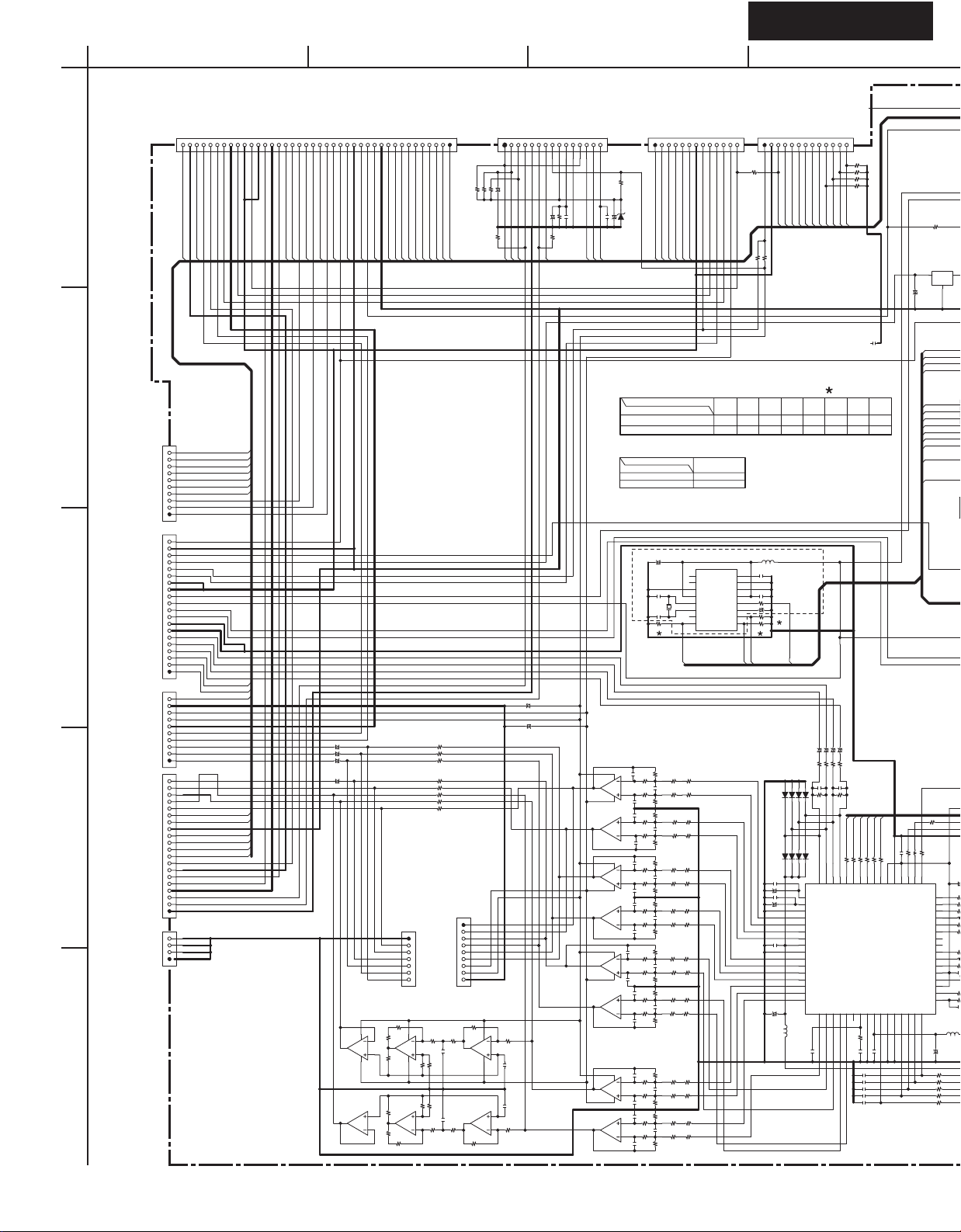
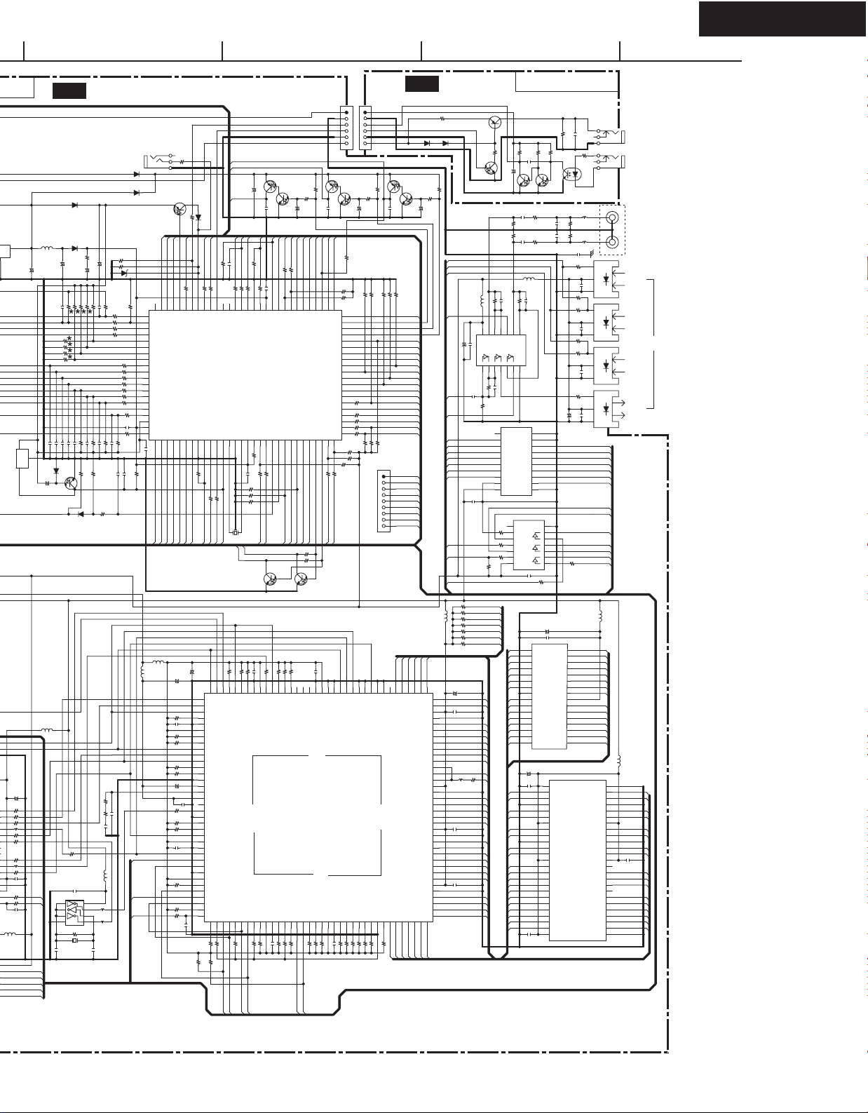
A
SCHEMATIC DIAGRAMS-2
DSP SECTION
1
2
TO NAAF-8523TO NAAF-8523TO NAAF-8523TO NAAF-8523
3
4
5
3938373635343332313029282726252423222120191817161514131211
40
P701A
GNDMIC
MICDET
+7V
OPTF
MICOUT
PROTECT
10
THERMAL
9
VOLH
8
SEC1H
7
APOWER
6
HPDET
5
VPOWER
4
FAC1
3
FAC2
2
-VP
1
P311A
+5VDIS
20
19
18
POFFV
+10S
17
16
15
14
GNDV
13
+12VTRG
12
+5VDSP
11
10
+3.3V
9
+2.5V
GNDDG
8
7
ADLT+
6
ADLT-
5
4
3
2
1
P302A
SBZ2MUT
10
GND+12V
9
-12VA
8
+12VA
7
GND+7
6
+7V
5
-7V
4
DAC_SR
3
DAC_SL
2
DAC_CT
1
P301A
20
19
18
17
DAC_SBR
16
FSWSDO
15
FSWCLK
14
13
GNDDG
12
FSWSTB
VOLSTB
11
VOLCLK
10
VOLDAT
9
MICOUT
8
GNDMIC
7
V4_R
6
V4_L
5
GNDV4A
4
3
TU_R
TU_L
2
GNDTU
1
P303A
4
3
2
1
E301
-7V
V4C
GND+7
VIDEO+5V/
SW+12V
VIDEO-5V
ADRT+
ADRTZ2MUT
AMUT
DAC_SW
DAC_SBL
DAC_FL
DAC_FR
V4Y
TO NADIS-8513
V4V
V4_L
GNDV4A
V4_R
FAC1
LEDSTBY
LEDPURE
VOLB
FAC2
VOLA
KEYINT3
-VP
C524
Q503:A
NJM4580M-D
Q503:B
NJM4580M-D
+5VDIS
C526
+
C525
+
C523
+
+
7
1
KEYINT2
GNDDG
10/50
40P
KEYINT1
8
4
+5.6DIS
BCDEFGH
NADG-8514
TO NAVD-8476TO NAVD-8476
KEYINT0
10/50
10/50
10/50
6
5
3
2
10
KEY3
GNDDG
R572
7
R582
NJM4580M-D
R581
1
R571
R561
987654321
FLDCS
FLDCLK
FLDSDO
KEY1
KEY0
KEY2
R596
R595
R593
R594
R597
R591
R592
R598
JL402B
NC
1
2
3
4
5
6
7
TO NAAF-8519
Q502:A
R562
NJM4580M-D
22K
R532
8
6
1.5K
22K
5
4
1.5K
22K
R552
Q502:B
22K
R551
3
1.5K
2
R531
1.5K
22K
22K
REMIN
FLDRST
LEDZONE2
R105 NC
0
0
0
0
0
NC
NC
0
P401A
NC
1
2
3
4
5
6
7
8
9
TO NAAF-8519
R512
10K
R522
7
1.5K
122J
C512
Q501:A
NJM4580M-D
22K
R542
Q501:B
NJM4580M-D
22K
R541
1
122J
C511
R521
10K
1.5K
R511
123456789
NC
+
C105
NC
R107NCR106
STEREO
NC
R104
8
R502
6
10K
5
4
C502
C501
3
10K
2
R501
SD
272J
272J
C531
C532
TUMUT
TU_R
+
FIL_FL
GNDTU
+
220/16
220/16
FIL_FR
TU_L
FIL_CT
DET
R103
FIL_SL
FIL_SW
C104
+
NC
NC
FIL_SR
1011121314
NC
NC
C103
R102
+12VA
FIL_SBL
FIL_SBR
Q401:B
NJM4580M-D
P101A
15
C102 NC
PLLCLK
PLLSDO
PLLCE
-12VA
7
Q404:A
NJM4580M-D
1
Q404:B
NJM4580M-D
7
Q403:A
NJM4580M-D
1
Q403:B
NJM4580M-D
7
Q402:A
NJM4580M-D
1
Q402:B
NJM4580M-D
Q401:A
NJM4580M-D
7
1
123456789
NC
P2004
NC
R101
NC
C101
+
+12VA
-12VA
NC
D101
OSDCS
FLDSDO
FLDCLK
Refer to following table about the parts displayed by mark " ".
DESTINATION
MPA, MWT, MGR, MGQ, MGK
MPP
CIRCUIT NO.
DESTINATION
MPP
Other
POFFV
+12VTRG
C111
+
100/16
C116
330J
C117
X111
330J
4.332MHz
R113
R478
4.7K
R438
180
8
4
8
4
8
4
8
4
R458
6
101J
C428
470
180
R468
5
472J
C408
R428
470
4.7K
101J
C418
R448
180
R427
R467
4.7K
3
681J
R447
C417
470
R477
2
472J
C407
180
R437
470
681J
C427
4.7K
R457
R436
R476
4.7K
R456
6
681J
C426
180
470
R466
5
472J
C406
R426
180
470
4.7K
681J
R446
C416
R425
R465
681J
3
6
4.7K
C415
R445
180
R475
472J
2
C405
180
R435
470
681J
C425
4.7K
R455
R434
470
R474
4.7K
R454
153J
C420
180
R464
5
333J
C404
R424
180
4.7K
470
153J
R444
C419
R423
C423
C422
C412
C411
C421
C413
470
4.7K
681J
R443
R463
180
472J
C403
R473
R433
180
470
681J
4.7K
R453
R432
R472
680
180
10K
R452
101
R422
NC
R462
680
C402
180
10K
101
R442
R421
680
R461
101
10K
R441
180
NC
C401
R431
R471
101
180
680
10K
R451
3
2
6
5
3
2
FSWSTB
FSWSDO
FSWCLK
VIDEO+5V/SW+12V
CIRCUIT NO.
R111,112,113
Q111 BU1924FS
9
T2
10
T1
11
VSS2
12
VDD2
13
XI
14
XO
15
NC
16
RCLK1QUAL
RDSCLK
R418
3.3K
R408
3.3K
R407
3.3K
R417
3.3K
R416
3.3K
R406
3.3K
R405
470
3.3K
R415
3.3K
R414
3.3K
R404
3.3K
R403
3.3K
R413
3.3K
R412
3.3K
R402
3.3K
R401
3.3K
R411
3.3K
V4Y
220K
000J
101112
VIDEO-5V
RDATA
R687
10K
10K
VSS3
VSS1
VDD1
V4C
CMP
MUX
1
2345678
13
P2005
R691
NC
V4V
-12VA
+12V/SW+12V
NC
0
R698
R699
R787
R686
10K
10K
10K
10K
L111
022M
8
7
6
5
4
+
3
Vref
2
R111
RDSSIG
RDSDAT
C303
104Z
C304
C305 NC
C306
100/16
C307
NC
C308
220/6.3
SDET
SYNC
VSYNC
R786
33K
33K
MPP Only
C115
561J
C113
104Z
1K
R114
C114
2.2/100
R112
DET
D302
D304
D303
D301
47/25
+
+
+
L302
022M
9
101112
13
R653
NC
R652
NC
R651
NC
R650
NC
VMUT
VCRST
VCSCL
VCSDA
SPRLZ2
SPRLSB
SPRLCS
SPRLF
C724
124J
R685
R785
R688
NO
10K
NO
56K
10/50
10/50
C323
C324
+
+
56
56
R324
R323
C325
222J
R325
3.9K
DIRINT_3V
DIRCS_3V
DIRRST_3V
220
220
220
R307
R308
R309
13
11
14
10
12
INT1
_RST
AINR-
AINL+
AINR+
Q421
CS42518/28-CQ
AOUTB2+:31
AOUTA2+:32
473K
C310
R788
10K
33K
C326
222J
R326
3.9K
DIGSDI_3V
DIGSDO_3V
220
220
R305
R306
9
8
CS/AD0
CDIN/AD1
CDOUT/SAD
64:CX_SDIN2
63:CX_SDIN3
62:CX_SDIN4
2.7K
R311
C311
C332
C333
C334
C335
C336
DIGCLK_3V
220
R304
7
6
CCLK/SCL
50:TXP
49:RXP0
104Z
330J
330J
330J
330J
330J
10K
10K
10/50
10/50
C322
C321
+
+
56
56
R321
R322
D306
D308
D305
D307
16
15
17
AINL-
VQ
18
FLT+
19
REFGND
20
AOUTB4-
21
AOUTB4+
22
AOUTA4+
23
AOUTA4-
24
VA
25
AGND1
26
AOUTB3-
27
AOUTB3+
28
AOUTA3+
29
AOUTA3-
30
AOUTB2-
31
32
AOUTA2-34AOUTB1-35AOUTB1+36AOUTA1+37AOUTA1-38MUTEC39LPFLT40AGND241VARX42RXP7/GP743RXP6/GP644RXP5/GP545RXP4/GP446RXP3/GP347RXP2/GP248RXP1/GP1
33
222J
C309
5
VLC
47
C302 NC
R303
3
4
VD1
DGND1
SAI_SLCK
SAI_LRCK
CX_SDOUT
SAI_SDOUT
CX_LRCK
0
R603
Q721
S812C56AUA-C3G-T2
IGO
+
C701
100/16
KEYINT3
KEYINT2
KEYINT1
KEYINT0
NC
Q702
R302
47
47
L312 LM182
R301
C301
220/6.3
1
2
+
R319
64
R318
63
R317
62
CX_SCLK
CX_SDIN1
L313
61
R315
60
R314
59
OMCK
58
ADCIN1
57
ADCIN2
R313
56
L311
55
RMCK
R312
54
C313
53
VLS
52
NC
DGND2
51
VD2
R331
330
50
R332
330
49
C331
330J
022M
L303
+
C312
220/6.3
R333
330
330
R334
R335
330
R336
330
R337
330
HPDET
MICDET
VOLB
VOLA
O
G
330
330
022M
L303
220/6.3
330
330
330
330
330
KEYINT3
KEYINT2
KEYINT1
KEYINT0
Q702
C301
220/6.3
R319
R318
R317
L313
R315
R314
R313
L311
R312
C313
NC
R331
R332
C331
330J
U03 DSP PC BOARD
+5VCPU
D702
1SS355
D701
1SS355
HPDET
MICDET
VOLB
VOLA
KEY3
KEY2
KEY1
KEY0
OSDCS
2
I
NC
O
1
+
C702
100/16
G
47
47
47
47
47
47
LM182
47
COAX1
OPT2
COAX2
OPT3
OPTF
+
3
TX
OPT1
C706
L701
470K
R785
R786
R787
R788
102K
C715
D703
+
1/50
RN1404
L301
022M
C703
100/16
102K
C716
1SS355
Q703
LM182
Q171
C172
+
10K
102K
R682
C714
102K
102K
C718
C717
R316
C171
TC7WU04FU
1
2
3
4
GND
R171
1M
12.288MHz
X171
120J
C704
R687
R688
2.7K
102K
R693
C719
D706
1SS355
47
104Z
VD
PCB
1K
R601
+
C705
+
DX-5R5L224
102K
R686
R685
C713
R782
R783
R784
INT3
INT2
INT1
BAND
2.7K
102K
102K
R694
C720
C721
1M
R602 10K
R604
R605
0
R257
R258
8
L172
7
LM182
6
L173
5
LM182
C173
+VCC
R674
100/16
UDZS5.1B
10K
1K
R781
R681
R789
R790
R791
R792
R793
R794
R795
4.7K
2.7K
R695
C722 102K
C710
330
2.7K
C205
680J
C206
L171
022M
120J
U07
JL121B
1
2
3
4
5
1K
R647
R747
2.2K
+
474K
C747
10/50
SPRLCS
PLLCLK
PLLSDO
PLLCE
TUMUT
SPRLF
56
575859606162636465
SPRLSB
SPRLCS
SPRLF/SPRLSW
TUMUT
PLLCE
PLLSDO
PLLCLK
FCE
VOLDAT
VOLCLK
VOLSTB
AMUT : 49
DSPRST
FEPM
DSPFINT
DSPINT
DSPBUSY
FCLK : 33
DIGCLK
FRXD : 32
DIGSDI
FTXD : 31
DIGSDO
~DIRRST
~DSPFCS
~DSPCS
VMUTMON
VMUTV1
VCTRLA
2526272829
10
10
R730
R729
VCSCL
DIRRST
DSPFCS
DSPCS
220
R727
R728
220
Q731
RN1404
C213
104Z
93
91
92
94
90
VSS1
VDD1
AUDATA6,GPIO30
AUDATA5,GPIO29
AUDATA7,XMT958B,GPIO31
SD_ADDR10,EXTA10
SD_ADDR4,EXTA4
SD_ADDR5,EXTA5
Q201
CS494003
SD_DATA6,EXTD6
SD_DATA5,EXTD5
SD_DATA4,EXTD4
SD_DATA3,EXTD3
C208
R218
R217
R216
10K
10K
10K
104Z
DSPFINT_3V
DSPFCS_3V
6
Q714
RN2402
Q713
C752
RN1404
NC
SPRLSB
R753
R658
NC
R659
NC
5152535455
50
49
48
--47
--46
45
44
43
42
41
40
39
38
37
R736
36
35
R734
34
R733
33
R732
32
R731
31
VCTRLB
30
R630
1K
R629
1K
R618
10K
VCSDA
88
85
87
86
NC289NC1
LRCLK1
SCLKN,GPIO22
LRCLKN,GPIO23
SD_BA,EXTA19
VDDSD1
VSSSD1
_SD_CS
VDDSD4
VSSSD4
SD_DQM0
R221
R220
R219
10K
10K
10K
C748
R222
10K
R748
10/50
2.2K
+
10K
R641
220
220
220
220
220
83
R223
10K
P721
R773
LEDSTBY
220K
80
NU
~LEDSTBY
HPRL
81
82
83
84
85
INIT3
86
INIT2
87
INIT1
88
BAND
89
~KEYINT3
90
~KEYINT2
91
~KEYINT1
92
~KEYINT0
93
KEY3
94
KEY2
95
KEY1
96
AVSS
97
98
99
100
FLDSDO
FLDCLK
123456789
C723
104Z
FLDCLK
FLDSDO
L202
022M
L201
022M
DACDA2
DACDA1
DACBCK
+PLLVDD
DACLRCK
ADSDO
SRCLRCK
R255
10K
R256
10K
104Z
DSPCLKIN
SRCDO
SRCBCK
330
Q705
RN2402
SYSOUT
LEDZONE2
LEDPURE
~SYSOUT
LEDPURE
81 : HPDET
82 : NU
83 : VOLB
84 : VOLA
97 : KEY0
98 : VREF
99 : AVCC
100 : NU
FLDCS
~FLDRST
FSWSDO
FLDCS
FLDRST
FSWSDO
C201
+
+VDSP
100/16
R249
10K
C215
104Z
R250
10K
R251
10K
C204
+
2.2M
C216
R259
R260
10K
R261
10K
C217
104Z
R266
10K
R269
3.3K
220
R270
C219
IRIN
1K
R774
RDSCLK
R7751K
FSWSTB
FSWSTB
FSWCLK
100/16
47
101J
R203
R201
RI
D712
D711
NC
R673
D707
NC
R683
1K
1K
1K
4.7K
4.7K
4.7K
4.7K
4.7K
4.7K
4.7K
R797
C709
104Z
2.7K
R800
220
R696
104Z
C711
104Z
R612 47K
122J
DSPCS_3V
DSPBUSY_3V D5
DSPRST_3V D3
Z2MUT
SBZ2MUT
+
C754
AMUT
D708
1SS355
SYSIN
22K
RDSDAT
RDSSIG
1K
1K
R772
R771
RDSSIG
SYSINNU~RDSCLK
M30622MGP-236FPU0
FSWCLK
BYTE
CNVSS
101112131415161718192021222324
10K
R708
220
R709
SDET
CNVSS
DACDA4
DACDA3
+
C202
108
109
110
111
112
113
114
115
116
117
CMPREQ,FLRCLKN2
118
CMPDAT,FSDATAN2
119
FLRCLKN1
120
_WR,_DS,GPIO10
121
_RD,R/_W,GPIO11
122
PLLVSS
123
FILT2
124
FILT1
125
PLLVDD
126
XTALO
127
CLKIN,XTALI
128
CLKSEL
129
_CS,GPIO9
130
A0,GPIO13
131
FSDATAN1
132
VDD4
133
VSS4
134
FSCLKN1,STCCLK2
135
_SCS
136
SCDIN
137
VSS5
138
VDD5
139
140
141
142
143
144
1
3.3K
3.3K
R202
3.3K
R215
22K
TRGZ2
VOLH
THERMAL
PROTECT
R663
R661
C712 104Z
1K
1K
1K
R763
R766
R765
R767
1K
67686970717273747576777879
66
SEC1H
VSS
VOLH
THERMAL
PROTECT
FANCTRL
FANHNURDSDAT
Q701
COMPA
COMPB
~RESET
XOUT
VSS
XIN
VCC1
~NMI
10K
R717
C707
104Z
RESET
R718 220
R624
220
R622
R621
R710
6.000MHz
SYNC
X701
VMUT
VCRST
10K
10K
10K
C214
104Z
R242
R239
R240
103
107
105
104
106
101
102
VSS2
SCLK0
LRCLK0
AUDATA2
HDATA4,GPIO4
HDATA3,GPIO3
AUDATA4,GPIO28
AUDATA3,XMT958A
109 :
110 :
111 :
112 :
113 :
114 :
115 :
116 :
139 :
140 :
141 :
142 :
143 :
144 :
UHS0,GPIO182UHS1,GPOI193_INTREQ4FA1,FSCDIN5GPOI206FA0,FSCCLK7FSCDIO,FSCDOUT
3.3K
DSPINT_3V
DIGSDO_3V
GPIO219FDAT710VDD611VSS612FHS0,_FWR,_FDS
8
10K
R208
R209
R205
10K
10K
DIGSDI_3V
DIGCLK_3V
Q712
RN2402
470/6.3
Q711
474K
C751
RN1404
SD
STEREO
220
220
SEC1H
APOWER
VPOWER
R759
R758
104Z
C708
~STEREO/PLLSDI
~SD
VPOWER
APOWER
VCC2
SPRLB : 50
FBUSY : 34
---
~REMIN
POFF
DIRINT1
DIRINT0
~DIRCS
POFF
220
R719
10K
10K
10K
DIRINT1
REMIN
DIRINT0
DIRCS
VSYNC
Q732
RN1404
10K
10K
47
R235
R234 10K
R238
R236
95
99
96
97
98
100
VDD2
MCLK
SCLK1
HDATA7,GPIO7
HDATA6,GPIO6
HDATA5,GPIO5
AUDATA1
AUDATA0
CMPCLK,FSCLKN2
HDATA2,GPIO2
VSS3
VDD3
HDATA3,GPIO3
HDATA0,GPIO0
A1, GPIO12
SCDOUT, SCDIO
HINBSY, GPIO8
SCCLK
UHS,_CS_OUT,GPIO17
_RESET
FSH1,_FRD,FR/_W
FDAT615_FCS16_FINTREQ17FDBCK18FDAT519FDAT420VDD721VSS722FDAT323FDBDA24FDAT225DBDA26DBCK27FDAT128TEST29FDAT030_NV_WE,GPIO16
13
14
C207104Z
R211
R210
R212
10K
3.3K
3.3K
IR IN TERMINAL PC BOARD
JL121A
+5.6IR
1
+12TRG
GNDTRG
2
3
IR_
TZ2
4
GNDIR
5
6
Q716
RN2402
1K
10K
R636
R648
10K
R639
P751A
10K
R631
474K
10K
R640
R632 10K
1
2
3
4
5
6
7
8
9
Q715
C753
RN1404
10K
R642
SPRLZ2
AMUTA
SBZ2MUTA
Z2MUTA
FCE
VOLDAT
VOLCLK
VOLSTB
DSPRST
FEPM
DSPFINT
DSPINT
DSPBUSY
DIGCLK
DIGSDI
DIGSDO
FBUSY
FCLK
FRXD
FTXD
10K
R646
RESET
CNVSS
FRXD
FCLK
+VCC
FBUSY
FTXD
GNDDG
APOWER
R749
2.2K
+
TO FLASH WRITER
A0A1A2A3RAS
CAS
80
81
82
78
79
73
74
75
76
77
NC484NC3
_SD_RAS
_SD_CAS
SDATAN3,GPIO27
SDATAN2,GPIO26
SDATAN1,GPIO25
SDATAN0,GPIO24
: 72
: 71
: 70
: 69
: 68
: 67
: 66
: 43
: 42
: 41
: 40
: 39
: 38
: 37
R224
10K
SD_ADDR3,EXTA3
SD_ADDR6,EXTA6
SD_CLK_EN
SD_ADDR7,EXTA7
SD_ADDR8,EXTA8
SD_CLK_IN
SD_ADDR9,EXTA9
SD_CLK_OUT
VDDSD2
VSSSD2
SD_ADAT8,EXTA11
SD_DATA9,EXTA11
SD_DATA10,EXTA13
SD_DATA11,EXTA14
SD_DATA12,EXTA15
VDDSD3
VSSSD3
SD_DATA13,EXTA16
SD_DATA14,EXTA17
SD_DATA15,EXTA18
SD_DQM1
SD_DATA7,EXTD7
_NV_OE,GPIO15
_NV_CS,GPIO14
_SD_WE34SD_DATA0,EXTD0
31
32
33
R22510K
BT_WE
BT_OE
BT_CS
SD_WED0D1
SD_ADDR1,EXTA1
SD_ADDR2,EXTA2
NC5
SD_DATA1,EXTD1
35
36
D2
R127
3.3
D122D121
1K
R649
C749
10/50
OPT1
OPT2
OPT3
TX
NC
NC
NC
L203
022M
NC
NC
NC
NC
+3.3DSPIO
C203
+
72
100/16
71
BA/EA19
C212
70
104Z
69
68
67
SD_ADDR0,EXTA0
66
65
64
63
62
61
60
L211
59
58
LL241
57
SD8/EA11
56
55
SD9/EA12
54
SD10/EA13
SD11/EA14
53
SD12/EA15
52
C210
51
104Z
50
SD13/EA16
49
48
47
SA14/EA17
SA15/EA18
46
SD_UDQM
45
44
43
C209
42
104Z
41
40
SD_LDQM
39
38
37
SD_DATA2,EXTD2
Q126
2SB1068
Q127
RN1402
L134
COAX1
104Z
+
C140
C139 100/16
C137
104K
DIRCS_3V
DIRRST_3V
DSPFCS_3V
DSPCS_3V
DIGSDO_3V
DIGCLK_3V
DSPRST_3V
C151
104Z
DSPINT_3V
DIGSDI_3V
DSPFINT_3V
CAS
R277
R276
R275
SD_CS
R274
SD_CKE
R273
SD_UDQM
R272
SD_LDQM
R271
A10
SD_CS
A4
A5
A6
SD_CKE
A7
A8
A9
R226
47
D7
D6
D4
1K
R128
C122
R133
220K
R137
220K
10K
080D
R134
022M
C133
10
12
14
11
13
IN5
IN6
VCC
OUT5
OUT6
1234567
R140
10K
C138
080D
220K
R139
COAX2
11
Y8
12
Y7
13
Y6
14
Y5
15
Y4
16
Y3
17
Y2
18
Y1
19
_G2
20
VCC1_G1
TC74HCT7007AF
8
R163
9
10
220
R164
11
220
12
R165
13
14
220
3.3K
R166
RAS
SD_WE
SD_CKO
NAETC-8518
R126
100K
C126
10K
3.3K
R123
R122
R124
10K
C121
223K
+
100/6.3
Q122
RN1402
Q123
RN1402
C132
104K
C135
104K
L133
022M
10K
R138
C136
8
9
IN4
OUT4
GND
GND
A8
A7
A6
A5
A4
Q151
A3
A2
A1
TC74VHC541FT
Q152
OUT4
IN4
OUT5
IN5
OUT6
IN6
VCC
C152
104Z
A3
A2
A1
A0
D0
D1
D2
D3
D4
D5
D6
D7
BT_CS
A10
BT_OE
C283
100/16
C284
104Z
SD_LDQM
SD_WE
SD_CS
BA/EA19
C287
104Z
R132
10
R136
10
080D
Q131
TC74HCU04AF
10
9
8
7
6
5
4
3
2
7
GND
6
5
4
3
2
1
R162
220
C281
100/16
+
C282
104Z
17
A3
18
A2
19
A1
20
A0
21
DQ0
22
DQ1
23
DQ2
24
VSS
A18/VPP
25
DQ3
26
_WE/A18
DQ4
27
DQ5
28
DQ6
29
DQ7
30
_CE
31
A10
32
_OE1A11
+
1
VCC0
D0
2
DQ0
D1
3
DQ1
4
GNDQ1
D2
5
DQ2
6
D3
DQ3
7
VCCQ1
8
D4
DQ4
9
D5
DQ5
10
GNDQ2
D6
11
DQ6
12
D7
DQ7
13
VCCQ2
14
LDQM
15
_WE
16
CAS
_CAS
RAS
17
_RAS
18
_CS
19
A11
A10
20
A10
A0
21
A0
A1
22
A1
A2
23
A2
A3
24
A3
25
VCC126GND1
C131
C134
Q121
PC817X
75
101J
R131
75
101J
R135
C146
104Z
R141
220
R145
NC
R142
220
R146
NC
R143
220
C143
R144
220
+
C145
100/16
R161
220
+VBOOT
16
A4
15
A5
14
A6
13
A7
12
SD9/EA12
A12
11
SD12/EA15
A15
10
SD13/EA16
A16
9
SA15/EA18
8
VCC
7
6
A17
5
A14
4
A13
3
A8
2
A9
P121
104Z
R121
100
P131
L131
022K
L132
022K
U131
IN
VCC
104Z
C141
GND
U132
IN
VCC
104Z
C142
GND
U133
IN
VCC
104Z
GND
U134
IN
VCC
104Z
C144
GND
DIRCS
DIRRST
DSPFCS
DSPCS
DIGSDO
DIGCLK
DSPRST
DIGSDI
DSPINT
DSPFINT
DIRINT0
DIRINT_3V
DSPBUSY
DSPBUSY_3V
022M
A4
A5
A6
A7
BT_WE
SA14/EA17
SD11/EA14
SD10/EA13
A8
A9
SD8/EA11
+VSD
GND2
DQ15
DQ14
GNDQ4
DQ13
DQ12
VCCQ4
DQ11
DQ10
GNDQ3
DQ9
DQ8
VCCQ3
NC2
IC42S16100
UDQM
CLK
CKE
NC1
Q282
A9
A8
A7
A6
A5
A4
12V TRIGGER
OUT
IR IN
IN 1
IN 2
IN 1
IN 2
IN 3
OUT
L281
Q281
L282
022M
50
SA15/EA18
49
SA14/EA17
48
47
46
SD13/EA16
SD12/EA15
45
44
SD11/EA14
43
42
SD10/EA13
41
40
SD9/EA12
39
SD8/EA11
C288
38
37
104Z
SD_UDQM
36
35
SD_CKO
34
SD_CKE
33
32
A9
A8
31
30
A7
A6
29
A5
28
27
A4
ZONE2
COAXIAL
DIGITAL
OPTICAL
MX26LV040-70
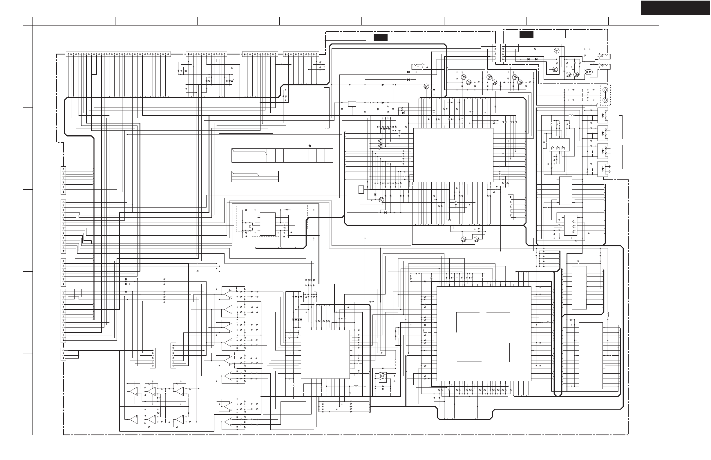
TX-SR603/603E/8360
A
SCHEMATIC DIAGRAMS-2
DSP SECTION
1
2
TO NAAF-8523TO NAAF-8523TO NAAF-8523TO NAAF-8523
3
4
5
3938373635343332313029282726252423222120191817161514131211
40
P701A
GNDMIC
MICDET
+7V
OPTF
MICOUT
PROTECT
10
THERMAL
9
VOLH
8
SEC1H
7
APOWER
6
HPDET
5
VPOWER
4
FAC1
3
FAC2
2
-VP
1
P311A
+5VDIS
20
19
18
POFFV
+10S
17
16
15
14
GNDV
13
+12VTRG
12
+5VDSP
11
10
+3.3V
9
+2.5V
GNDDG
8
7
ADLT+
6
ADLT-
5
4
3
2
1
P302A
SBZ2MUT
10
GND+12V
9
-12VA
8
+12VA
7
GND+7
6
+7V
5
-7V
4
DAC_SR
3
DAC_SL
2
DAC_CT
1
P301A
20
19
18
17
DAC_SBR
16
FSWSDO
15
FSWCLK
14
13
GNDDG
12
FSWSTB
VOLSTB
11
VOLCLK
10
VOLDAT
9
MICOUT
8
GNDMIC
7
V4_R
6
V4_L
5
GNDV4A
4
3
TU_R
TU_L
2
GNDTU
1
P303A
4
3
2
1
E301
-7V
V4C
GND+7
VIDEO+5V/
SW+12V
VIDEO-5V
ADRT+
ADRTZ2MUT
AMUT
DAC_SW
DAC_SBL
DAC_FL
DAC_FR
V4Y
TO NADIS-8513
V4V
V4_L
GNDV4A
V4_R
FAC1
LEDSTBY
LEDPURE
VOLB
FAC2
VOLA
KEYINT3
-VP
C524
Q503:A
NJM4580M-D
Q503:B
NJM4580M-D
+5VDIS
C526
+
C525
+
C523
+
+
7
1
KEYINT2
GNDDG
10/50
40P
KEYINT1
8
4
+5.6DIS
BCDEFGH
KEYINT0
10/50
10/50
10/50
6
5
3
2
10
KEY3
GNDDG
R572
7
R582
NJM4580M-D
R581
1
R571
R561
987654321
FLDCS
FLDCLK
FLDSDO
KEY1
KEY0
KEY2
R596
R595
R593
R594
R597
R591
R592
R598
JL402B
NC
1
2
3
4
5
6
7
TO NAAF-8519
Q502:A
R562
NJM4580M-D
22K
R532
8
6
1.5K
22K
5
4
1.5K
22K
R552
Q502:B
22K
R551
3
1.5K
2
R531
1.5K
22K
22K
REMIN
FLDRST
LEDZONE2
R105 NC
0
0
0
0
0
NC
NC
0
P401A
NC
1
2
3
4
5
6
7
8
9
TO NAAF-8519
R512
10K
R522
7
1.5K
122J
C512
Q501:A
NJM4580M-D
22K
R542
Q501:B
NJM4580M-D
22K
R541
1
122J
C511
R521
10K
1.5K
R511
123456789
NC
+
C105
NC
R107NCR106
STEREO
NC
R104
8
R502
6
10K
5
4
C502
C501
3
10K
2
R501
SD
272J
272J
C531
C532
TUMUT
TU_R
FIL_FL
+
GNDTU
+
220/16
220/16
FIL_FR
TU_L
FIL_CT
DET
R103
FIL_SL
FIL_SW
C104
+
NC
NC
FIL_SR
1011121314
NC
NC
C103
R102
+12VA
FIL_SBL
FIL_SBR
Q401:B
NJM4580M-D
P101A
15
C102 NC
PLLCLK
PLLSDO
PLLCE
-12VA
7
Q404:A
NJM4580M-D
1
Q404:B
NJM4580M-D
7
Q403:A
NJM4580M-D
1
Q403:B
NJM4580M-D
7
Q402:A
NJM4580M-D
1
Q402:B
NJM4580M-D
Q401:A
NJM4580M-D
7
1
123456789
NC
P2004
NC
R101
NC
C101
+
+12VA
-12VA
NC
D101
OSDCS
FLDSDO
FLDCLK
Refer to following table about the parts displayed by mark " ".
DESTINATION
MPA, MWT, MGR, MGQ, MGK
MPP
CIRCUIT NO.
DESTINATION
MPP
Other
POFFV
+12VTRG
C111
+
100/16
C116
330J
C117
X111
330J
4.332MHz
R113
R478
4.7K
R438
180
8
4
8
4
8
4
8
4
R458
6
101J
C428
470
180
R468
5
472J
C408
R428
470
4.7K
101J
C418
R448
180
R427
R467
4.7K
3
681J
R447
C417
470
R477
2
472J
C407
180
R437
470
681J
C427
4.7K
R457
R436
R476
4.7K
R456
6
681J
C426
180
470
R466
5
472J
C406
R426
180
470
4.7K
681J
R446
C416
R425
R465
681J
3
6
4.7K
C415
R445
180
470
R475
472J
2
C405
180
R435
470
681J
C425
4.7K
R455
R434
470
R474
4.7K
R454
153J
C420
180
R464
5
333J
C404
R424
180
4.7K
470
153J
R444
C419
R423
C423
C422
C412
C411
C421
C413
470
4.7K
681J
R443
R463
180
472J
C403
R473
R433
180
470
681J
4.7K
R453
R432
R472
680
180
10K
R452
101
R422
NC
R462
680
C402
180
10K
101
R442
R421
680
R461
101
10K
R441
180
NC
C401
R431
R471
101
180
680
10K
R451
3
2
6
5
3
2
FSWSTB
FSWSDO
FSWCLK
VIDEO+5V/SW+12V
CIRCUIT NO.
R111,112,113
Q111 BU1924FS
9
T2
10
T1
11
VSS2
12
VDD2
13
XI
14
XO
15
NC
16
RCLK1QUAL
RDSCLK
R418
3.3K
R408
3.3K
R407
3.3K
R417
3.3K
R416
3.3K
R406
3.3K
R405
3.3K
R415
3.3K
R414
3.3K
R404
3.3K
R403
3.3K
R413
3.3K
R412
3.3K
R402
3.3K
R401
3.3K
R411
3.3K
V4Y
220K
000J
101112
V4C
VIDEO-5V
-12VA
R687
10K
10K
CMP
VSS3
VSS1
VDD1
MUX
Vref
RDATA
13
V4V
8
7
6
5
4
3
2
R787
R691
NC
10K
10K
RDSSIG
RDSDAT
TO NAVD-8476TO NAVD-8476
1
P2005
+12V/SW+12V
NC
0
R698
R699
R686
10K
10K
L111
022M
+
R111
C303
104Z
C304
C305 NC
C306
100/16
C307
NC
C308
220/6.3
2345678
VCSDA
SDET
SYNC
VSYNC
R786
33K
33K
MPP Only
C115
561J
C113
104Z
1K
R114
C114
2.2/100
R112
DET
D302
D304
D306
D303
D305
D301
47/25
+
17
18
+
19
20
21
22
23
24
25
26
27
28
29
30
31
32
+
L302
022M
NADG-8514
9
101112
13
R653
NC
R652
NC
R651
NC
R650
NC
VMUT
VCRST
VCSCL
SPRLZ2
SPRLSB
SPRLCS
SPRLF
C724
124J
R685
R785
R688
NO
10K
NO
56K
10/50
10/50
C323
C324
+
+
56
56
R324
R323
C325
222J
R325
3.9K
DIRINT_3V
DIRCS_3V
DIRRST_3V
220
220
220
R307
R308
R309
13
11
14
10
12
INT1
_RST
AINR-
AINL+
AINR+
Q421
CS42518/28-CQ
AOUTB2+:31
AOUTA2+:32
473K
C310
R788
10K
33K
C326
222J
R326
3.9K
DIGSDI_3V
DIGSDO_3V
220
220
R305
R306
9
8
CS/AD0
CDIN/AD1
CDOUT/SAD
64:CX_SDIN2
63:CX_SDIN3
62:CX_SDIN4
2.7K
R311
C311
C332
C333
C334
C335
C336
DIGCLK_3V
220
R304
5
7
6
VLC
CCLK/SCL
50:TXP
49:RXP0
104Z
330J
330J
330J
330J
330J
C302 NC
4
DGND1
10K
10K
10/50
10/50
C322
C321
+
+
56
56
R321
R322
D308
D307
16
15
AINL-
VQ
FLT+
REFGND
AOUTB4AOUTB4+
AOUTA4+
AOUTA4VA
AGND1
AOUTB3AOUTB3+
AOUTA3+
AOUTA3AOUTB2-
AOUTA2-34AOUTB1-35AOUTB1+36AOUTA1+37AOUTA1-38MUTEC39LPFLT40AGND241VARX42RXP7/GP743RXP6/GP644RXP5/GP545RXP4/GP446RXP3/GP347RXP2/GP248RXP1/GP1
33
222J
C309
0
R603
Q721
S812C56AUA-C3G-T2
IGO
+
C701
100/16
R302
47
47
47
L312 LM182
R301
R303
3
1
2
VD1
64
63
62
CX_SCLK
CX_LRCK
CX_SDIN1
61
SAI_SLCK
60
SAI_LRCK
59
OMCK
58
ADCIN1
57
ADCIN2
56
CX_SDOUT
55
RMCK
54
SAI_SDOUT
53
VLS
52
DGND2
51
VD2
50
49
+
C312
R333
R334
R335
R336
R337
330
330
022M
L303
220/6.3
330
330
330
330
330
KEYINT3
KEYINT2
KEYINT1
KEYINT0
Q702
C301
220/6.3
R319
R318
R317
L313
R315
R314
R313
L311
R312
C313
NC
R331
R332
C331
330J
U03 DSP PC BOARD
+5VCPU
D702
1SS355
D701
1SS355
HPDET
MICDET
VOLB
VOLA
KEY3
KEY2
KEY1
KEY0
OSDCS
2
I
NC
O
1
+
C702
100/16
G
47
47
47
47
47
47
LM182
47
COAX1
OPT2
COAX2
OPT3
OPTF
+
3
TX
OPT1
C706
L701
470K
R785
R786
R787
R788
102K
C715
D703
+
1/50
RN1404
L301
022M
C703
100/16
102K
C716
1SS355
Q703
LM182
Q171
C172
+
10K
102K
R688
R682
C714
102K
102K
102K
C718
C717
C719
1SS355
R316
47
C171
TC7WU04FU
1
2
3
4
GND
R171
1M
12.288MHz
X171
120J
C704
DX-5R5L224
R686
R687
2.7K
102K
R693
C720
R602 10K
D706
104Z
VD
PCB
1K
R601
+VCC
R674
+
C705
+
100/16
UDZS5.1B
10K
102K
R685
1K
R781
R681
C713
R782
R783
R784
INT3
INT2
INT1
BAND
R789
R790
R791
R792
R793
R794
R795
4.7K
2.7K
2.7K
102K
R694
R695
C721
C722 102K
1M
C710
R604
R605
0
330
R257
2.7K
R258
C205
680J
C206
L171
022M
8
L172
7
LM182
6
L173
5
LM182
120J
C173
U07
JL121B
1
2
3
4
5
P721
R773
LEDSTBY
220K
80
NU
~LEDSTBY
HPRL
81
82
83
84
85
INIT3
86
INIT2
87
INIT1
88
BAND
89
~KEYINT3
90
~KEYINT2
91
~KEYINT1
92
~KEYINT0
93
KEY3
94
KEY2
95
KEY1
96
AVSS
97
98
99
100
FLDSDO
FLDCLK
123456789
C723
104Z
FLDCLK
FLDSDO
L202
022M
L201
022M
DACDA2
DACDA1
DACBCK
+PLLVDD
DACLRCK
ADSDO
SRCLRCK
R255
10K
R256
10K
104Z
DSPCLKIN
SRCDO
SRCBCK
330
Q705
RN2402
SYSOUT
LEDZONE2
LEDPURE
~SYSOUT
LEDPURE
81 : HPDET
82 : NU
83 : VOLB
84 : VOLA
97 : KEY0
98 : VREF
99 : AVCC
100 : NU
FLDCS
~FLDRST
FSWSDO
FLDCS
FLDRST
FSWSDO
C201
+
+VDSP
100/16
R249
10K
C215
104Z
R250
10K
R251
10K
C204
+
2.2M
C216
R259
R260
10K
R261
10K
C217
104Z
R266
10K
R269
3.3K
220
R270
C219
IRIN
1K
R774
RDSCLK
R7751K
FSWSTB
FSWSTB
FSWCLK
100/16
47
101J
R203
R201
RI
D712
D711
NC
R673
D707
NC
R683
1K
1K
1K
4.7K
4.7K
4.7K
4.7K
4.7K
4.7K
4.7K
R797
C709
104Z
2.7K
R800
220
R696
104Z
C711
104Z
R612 47K
122J
DSPCS_3V
DSPBUSY_3V D5
DSPRST_3V D3
Z2MUT
SBZ2MUT
+
C754
470/6.3
AMUT
D708
1SS355
SYSIN
22K
RDSDAT
RDSSIG
1K
1K
R772
R771
RDSSIG
SYSINNU~RDSCLK
M30622MGP-236FPU0
FSWCLK
BYTE
CNVSS
101112131415161718192021222324
10K
R708
220
R709
SDET
CNVSS
DACDA4
DACDA3
+
C202
108
109
110
111
112
113
114
115
116
117
CMPREQ,FLRCLKN2
118
CMPDAT,FSDATAN2
119
FLRCLKN1
120
_WR,_DS,GPIO10
121
_RD,R/_W,GPIO11
122
PLLVSS
123
FILT2
124
FILT1
125
PLLVDD
126
XTALO
127
CLKIN,XTALI
128
CLKSEL
129
_CS,GPIO9
130
A0,GPIO13
131
FSDATAN1
132
VDD4
133
VSS4
134
FSCLKN1,STCCLK2
135
_SCS
136
SCDIN
137
VSS5
138
VDD5
139
140
141
142
143
144
1
3.3K
3.3K
R202
3.3K
R215
22K
TRGZ2
R661
FANHNURDSDAT
PROTECT
C712 104Z
1K
R767
67686970717273747576777879
PROTECT
FANCTRL
VOLH
THERMAL
1K
1K
R766
R765
66
VSS
VOLH
THERMAL
R663
SEC1H
R763
1K
SEC1H
Q701
COMPA
COMPB
~RESET
XOUT
VSS
XIN
VCC1
~NMI
10K
R717
C707
104Z
RESET
R718 220
R624
R622
R621
6.000MHz
X701
VMUT
VCRST
10K
10K
R242
R239
R240
103
105
104
106
102
SCLK0
AUDATA2
HDATA4,GPIO4
HDATA3,GPIO3
AUDATA3,XMT958A
10K
R205
DIGSDI_3V
DSPINT_3V
DIGCLK_3V
DIGSDO_3V
10K
10K
10K
VSYNC
10K
C214
104Z
101
100
VSS2
AUDATA4,GPIO28
109 :
110 :
111 :
112 :
113 :
114 :
115 :
116 :
139 :
140 :
141 :
142 :
143 :
144 :
GPIO219FDAT710VDD611VSS612FHS0,_FWR,_FDS
8
R208
R209
10K
10K
220
R710
SYNC
107
LRCLK0
UHS0,GPIO182UHS1,GPOI193_INTREQ4FA1,FSCDIN5GPOI206FA0,FSCCLK7FSCDIO,FSCDOUT
3.3K
Q712
RN2402
Q711
474K
C751
RN1404
SD
STEREO
220
220
APOWER
VPOWER
R759
R758
104Z
C708
~STEREO/PLLSDI
~SD
VPOWER
APOWER
VCC2
FBUSY : 34
---
~REMIN
POFF
DIRINT1
DIRINT0
~DIRCS
POFF
220
R719
DIRINT1
REMIN
DIRINT0
DIRCS
Q732
RN1404
10K
10K
47
R235
R234 10K
R238
R236
95
99
96
97
98
VDD2
MCLK
SCLK1
HDATA6,GPIO6
HDATA5,GPIO5
AUDATA1
AUDATA0
CMPCLK,FSCLKN2
HDATA2,GPIO2
VSS3
VDD3
HDATA3,GPIO3
HDATA0,GPIO0
A1, GPIO12
SCDOUT, SCDIO
HINBSY, GPIO8
SCCLK
UHS,_CS_OUT,GPIO17
_RESET
FSH1,_FRD,FR/_W
13
14
C207104Z
R211
R210
R212
10K
3.3K
3.3K
6
Q714
RN2402
1K
R647
R747
2.2K
+
C747
10/50
PLLCLK
PLLSDO
PLLCE
TUMUT
SPRLF
56
575859606162636465
SPRLF/SPRLSW
TUMUT
PLLCE
PLLSDO
PLLCLK
SPRLB : 50
AMUT : 49
DSPRST
DSPFINT
DSPBUSY
FCLK : 33
FRXD : 32
FTXD : 31
~DIRRST
~DSPFCS
~DSPCS
VMUTMON
2526272829
DIRRST
DSPFCS
DSPCS
R727
R728
Q731
RN1404
C213
104Z
93
91
92
94
90
VSS1
HDATA7,GPIO7
AUDATA6,GPIO30
AUDATA5,GPIO29
AUDATA7,XMT958B,GPIO31
Q201
CS494003
FDAT615_FCS16_FINTREQ17FDBCK18FDAT519FDAT420VDD721VSS722FDAT323FDBDA24FDAT225DBDA26DBCK27FDAT128TEST29FDAT030_NV_WE,GPIO16
R218
R217
R216
10K
10K
10K
DSPFINT_3V
DSPFCS_3V
C748
+
Q713
474K
C752
RN1404
NC
SPRLCS
SPRLSB
R753
R658
NC
R659
NC
5152535455
SPRLSB
SPRLCS
50
49
48
--47
--46
FCE
45
VOLDAT
44
VOLCLK
43
VOLSTB
42
41
FEPM
40
39
DSPINT
38
37
DIGCLK
R736
36
DIGSDI
35
DIGSDO
R734
34
R733
33
R732
32
R731
31
VMUTV1
VCTRLA
VCTRLB
30
R630
1K
R629
1K
R618
10
10
10K
R730
R729
VCSDA
VCSCL
220
220
88
85
87
86
NC289NC1
VDD1
LRCLK1
SCLKN,GPIO22
LRCLKN,GPIO23
SD_ADDR10,EXTA10
SD_BA,EXTA19
VDDSD1
VSSSD1
_SD_CS
SD_ADDR4,EXTA4
SD_ADDR5,EXTA5
SD_DATA6,EXTD6
VDDSD4
VSSSD4
SD_DATA5,EXTD5
SD_DQM0
SD_DATA4,EXTD4
SD_DATA3,EXTD3
C208
R222
R221
R220
R219
10K
10K
10K
10K
104Z
10/50
220
220
220
220
220
R748
2.2K
10K
R641
83
R223
10K
IR IN TERMINAL PC BOARD
JL121A
+5.6IR
1
+12TRG
GNDTRG
2
3
IR_
TZ2
4
GNDIR
5
6
Q716
RN2402
1K
10K
R636
R648
10K
P751A
R639
10K
R631
474K
10K
R640
R632 10K
C753
10K
R642
1
2
3
4
5
6
7
8
9
Q715
RN1404
SPRLZ2
AMUTA
SBZ2MUTA
Z2MUTA
FCE
VOLDAT
VOLCLK
VOLSTB
DSPRST
FEPM
DSPFINT
DSPINT
DSPBUSY
DIGCLK
DIGSDI
DIGSDO
FBUSY
FCLK
FRXD
FTXD
10K
R646
RESET
CNVSS
FRXD
FCLK
+VCC
FBUSY
FTXD
GNDDG
APOWER
R749
2.2K
+
TO FLASH WRITER
A0A1A2A3RAS
CAS
80
81
82
78
79
73
74
75
76
77
NC484NC3
_SD_RAS
_SD_CAS
SDATAN3,GPIO27
SDATAN2,GPIO26
SDATAN1,GPIO25
SDATAN0,GPIO24
: 72
: 71
: 70
: 69
: 68
: 67
: 66
: 43
: 42
: 41
: 40
: 39
: 38
: 37
R224
10K
SD_ADDR3,EXTA3
SD_ADDR6,EXTA6
SD_CLK_EN
SD_ADDR7,EXTA7
SD_ADDR8,EXTA8
SD_CLK_IN
SD_ADDR9,EXTA9
SD_CLK_OUT
VDDSD2
VSSSD2
SD_ADAT8,EXTA11
SD_DATA9,EXTA11
SD_DATA10,EXTA13
SD_DATA11,EXTA14
SD_DATA12,EXTA15
VDDSD3
VSSSD3
SD_DATA13,EXTA16
SD_DATA14,EXTA17
SD_DATA15,EXTA18
SD_DQM1
SD_DATA7,EXTD7
_NV_OE,GPIO15
_NV_CS,GPIO14
_SD_WE34SD_DATA0,EXTD0
31
32
33
R22510K
BT_WE
BT_OE
BT_CS
SD_WED0D1
SD_ADDR1,EXTA1
SD_ADDR2,EXTA2
NC5
SD_DATA1,EXTD1
35
36
D2
R127
3.3
D122D121
1K
R649
C749
10/50
OPT1
OPT2
OPT3
TX
DIRCS_3V
DIRRST_3V
DSPFCS_3V
DSPCS_3V
DIGSDO_3V
DIGCLK_3V
DSPRST_3V
NC
NC
NC
L203
022M
NC
NC
NC
NC
+3.3DSPIO
C203
+
72
100/16
71
BA/EA19
C212
70
104Z
69
68
67
SD_ADDR0,EXTA0
66
65
64
SD_CKE
63
62
61
60
L211
59
58
LL241
57
SD8/EA11
56
55
SD9/EA12
54
SD10/EA13
SD11/EA14
53
SD12/EA15
52
C210
51
104Z
50
SD13/EA16
49
48
47
SA14/EA17
SA15/EA18
46
SD_UDQM
45
44
43
C209
42
104Z
41
40
SD_LDQM
39
38
37
SD_DATA2,EXTD2
Q126
2SB1068
Q127
RN1402
L134
COAX1
104Z
+
C140
C139 100/16
C137
104K
C151
104Z
DSPINT_3V
DIGSDI_3V
DSPFINT_3V
CAS
R277
R276
R275
SD_CS
R274
SD_CKE
R273
SD_UDQM
R272
SD_LDQM
R271
A10
SD_CS
A4
A5
A6
A7
A8
A9
R226
47
D7
D6
D4
1K
R128
C122
100/6.3
R133
220K
R137
220K
10K
080D
R134
022M
C133
10
12
14
11
13
IN5
IN6
VCC
OUT5
OUT6
1234567
R140
10K
C138
080D
220K
R139
COAX2
11
Y8
12
Y7
13
Y6
14
Y5
15
Y4
16
Y3
17
Y2
18
Y1
19
_G2
20
VCC1_G1
TC74HCT7007AF
8
R163
9
10
220
R164
11
220
12
R165
13
14
220
3.3K
R166
RAS
SD_WE
A3
A2
A1
A0
D0
D1
D2
D3
D4
D5
D6
D7
BT_CS
A10
BT_OE
SD_CKO
R124
+
C132
104K
C135
104K
10K
R138
8
9
IN4
Q151
Q152
OUT4
IN4
OUT5
IN5
OUT6
IN6
VCC
C152
104Z
SD_LDQM
SD_WE
SD_CS
BA/EA19
NAETC-8518
R126
100K
104Z
C126
R121
10K
3.3K
R123
R122
10K
C121
223K
Q123
RN1402
R132
10
R136
10
L133
022M
080D
C136
OUT4
GND
Q131
TC74HCU04AF
10
GND
9
A8
8
A7
7
A6
6
A5
5
A4
4
A3
3
A2
2
A1
TC74VHC541FT
GND
R162
220
100/16
17
A3
18
A2
19
A1
20
A0
21
DQ0
22
DQ1
23
DQ2
24
VSS
25
DQ3
26
DQ4
27
DQ5
28
DQ6
29
DQ7
30
_CE
31
A10
32
_OE1A11
C283
100/16
+
C284
104Z
D0
D1
D2
D3
D4
D5
D6
D7
CAS
RAS
A10
A0
A1
A2
A3
C287
104Z
Q122
RN1402
Q121
PC817X
101J
C131
R131
101J
R135
C134
C146
104Z
+
C145
100/16
7
6
5
4
3
2
R161
1
220
C281
+
C282
104Z
16
A4
15
A5
14
A6
13
A7
12
A12
11
A15
10
A16
9
A18/VPP
8
VCC
7
_WE/A18
6
A17
5
A14
4
A13
3
A8
2
A9
1
VCC0
2
DQ0
3
DQ1
4
GNDQ1
5
DQ2
6
DQ3
7
VCCQ1
8
DQ4
9
DQ5
10
GNDQ2
11
DQ6
12
DQ7
13
VCCQ2
14
LDQM
15
_WE
16
_CAS
17
_RAS
18
_CS
19
A11
20
A10
21
A0
22
A1
23
A2
24
A3
25
VCC126GND1
100
P131
L131
022K
75
75
L132
022K
R141
220
104Z
C141
R145
NC
R142
220
104Z
C142
R146
NC
R143
220
104Z
C143
R144
220
104Z
C144
DIRCS
DIRRST
DSPFCS
DSPCS
DIGSDO
DIGCLK
DSPRST
DIGSDI
DSPINT
DSPFINT
DIRINT0
DIRINT_3V
DSPBUSY
DSPBUSY_3V
+VBOOT
A4
A5
A6
A7
SD9/EA12
SD12/EA15
SD13/EA16
SA15/EA18
BT_WE
SA14/EA17
SD11/EA14
SD10/EA13
SD8/EA11
GND2
GNDQ4
VCCQ4
GNDQ3
VCCQ3
IC42S16100
UDQM
Q282
DQ15
DQ14
DQ13
DQ12
DQ11
DQ10
IN
VCC
GND
IN
VCC
GND
IN
VCC
GND
IN
VCC
GND
A8
A9
+VSD
DQ9
DQ8
NC2
CLK
CKE
NC1
U134
022M
A9
A8
A7
A6
A5
A4
U133
P121
U131
U132
L281
50
49
48
47
46
45
44
43
42
41
40
39
38
37
36
35
34
33
32
31
30
29
28
27
SD_UDQM
12V TRIGGER
OUT
ZONE2
IR IN
IN 1
COAXIAL
IN 2
DIGITAL
IN 1
IN 2
OPTICAL
IN 3
OUT
Q281
MX26LV040-70
L282
022M
SA15/EA18
SA14/EA17
SD13/EA16
SD12/EA15
SD11/EA14
SD10/EA13
SD9/EA12
SD8/EA11
C288
104Z
SD_CKO
SD_CKE
A9
A8
A7
A6
A5
A4

TX-SR603/603E/8360 TX-SR603/603E/8360
A
SCHEMATIC DIAGRAMS-3
POWER AMPLIFIER SECTION-1
1
Refer to following table about the parts displayed by mark " ".
Transistors
CIRCUIT NO.
Q5000 - 5002
Q5010 - 5012
Q5003 - 5006
Q5013 - 5016
Q5030 -5036
Q5040 - 5046
Q5050 - 5056
NOTE
2
THE COMPONENTS IDENTIFIED BY MARK ARE CRITICAL FOR SAFETY
REPLACE ONLY WITH PART NUMBER SPECIFIED.
VOLTAGE (MEASURED WITH VOLTMETER) IS DC VOLTAGE.(NO INPUT SIGNAL).
ALL PNP TRANSISTORS ARE EQUIVALENT TO 2SA1015-GR UNLESS OTHERWISE NOTED.
ALL NPN TRANSISTORS ARE EQUIVALENT TO 2SC1815-GR UNLESS OTHERWISE NOTED.
ALL DIODES ARE EQUIVALENT TO 1SS133 UNLESS OTHERWISE NOTED.
ELECTROLYTIC CAPACITORS ( ) ARE IN uF/WV.
ALL CAPACITORS ARE IN pF/50WV UNLESS OTHERWISE NOTED.
EX) 030- 3pF 330- 33pF 331- 330pF 333- 0.033uF
ALL RESISTORS ARE IN OHMS 1/4WATTS UNLESS OTHERWISE NOTED.
THE THICK LINES ON PC BOARD ARE THE PRINTING SIDE OF THE PARTS.
EX) PRINTING SIDE
CIRCUIT IS SUBJECT TO CHANGE FOR IMPROVEMENT.
<Note>
NC=No mount of parts.
3
DESCRIPTION
2SC2240-BL
2SC2240-BL, KTC3200-BL
2SA949-Y
2SC2229-Y
2SC2240-GR, BL
!
BCDEFGH
18K
R5163
100
(1/4W)
52.5V
C5083
040C
C5093
101K
(1/4W)
C5084
040C
C5094
101K
R5233
R5234
1.1V
R5033
120K
-1.1V
Q5043
R5173
100
(1/4W)
52.5V
1.1V
R5034
120K
-1.1V
R5174
100
(1/4W)
Q5033
C5053
47/50
120K
Q5034
C5054
47/50
120K
Q5044
R5203
NC
R5204
NC
(1/4W)
P6003A
(1/4W)
P6004A
52.0V
0V
-52.2V
R5164
100
52.0V
0V
-52.2V
SL
R5003
1K
C5003
101K
R5043
D5003
MTZJ5.6B
DZ-5.6BSB
SR
R5004
1K
C5004
101K
R5044 2.2K
D5004
MTZJ5.6B
DZ-5.6BSB
C5013
10/50
2.2K
C5014
10/50
R5013
56K
R5014
56K
R5093
100K
-0.1V
R5023
330
-47.5V
R5103
100K
R5094
100K
-0.1V
R5024
330
-47.5V
R5104
100K
R5113
1K
C5033
Q5003 Q5013
-0.65V
C5023
10/50
R5114
C5034
Q5004 Q5014
-0.65V
C5024
10/50
51.5V
NC
R5053
4.7K
Q5053
-48.1V
R5063
1.2K
R5073
NC
1K
NC
R5054
4.7K
Q5054
-48.1V
R5064
1.2K
R5074
NC
R5083
470
51.5V
R5084
470
C5043
220/25
C5044
220/25
C5103
10/100
C5113
10/100
-51.7V
C5104
10/100
C5114
10/100
R5133
18K
R5134
-51.7V
18K
18K
R5165
(1/4W)
100
52.0V
0V
100
52.0V
0V
C5085
040C
C5095
101K
-52.2V
R5166
(1/4W)
C5086
040C
C5096
101K
-52.2V
R5235
R5236
52.5V
1.1V
R5035
120K
-1.1V
R5175
100
(1/4W)
52.5V
1.1V
R5036
120K
-1.1V
R5176
100
(1/4W)
Q5035
C5055
47/50
120K
Q5045
Q5036
C5056
47/50
120K
Q5046
R5205
NC
R5206
NC
(1/4W)
P6005A
(1/4W)
JL6006A
SBL
C5015
R5005
10/50
1K
R5015
2.2K
56K
R5025
R5105
C5005
101K
4
R5045
D5005
MTZJ5.6B
DZ-5.6BSB
SBR
C5016
R5006
10/50
1K
R5016
C5006
101K
56K
R5026
5
2.2K
R5046
D5006
MTZJ5.6B
DZ-5.6BSB
R5106
R5095
100K
-0.1V
330
-47.5V
100K
R5096
100K
-0.1V
330
-47.5V
100K
C5035
Q5005
-0.65V
C5025
10/50
R5116
1K
Q5006 Q5016
-0.65V
C5026
10/50
R5115
1K
NC
C5036
NC
R5055
4.7K
Q5055
-48.1V
R5065
1.2K
R5075
NC
R5056
4.7K
Q5056
-48.1V
R5066
1.2K
R5076
NC
Q5015
51.5V
R5085
51.5V
R5086
C5045
220/25
470
C5046
220/25
470
C5105
10/100
R5135
C5115
10/100
-51.7V
C5106
10/100
C5116
10/100
-51.7V
R5136
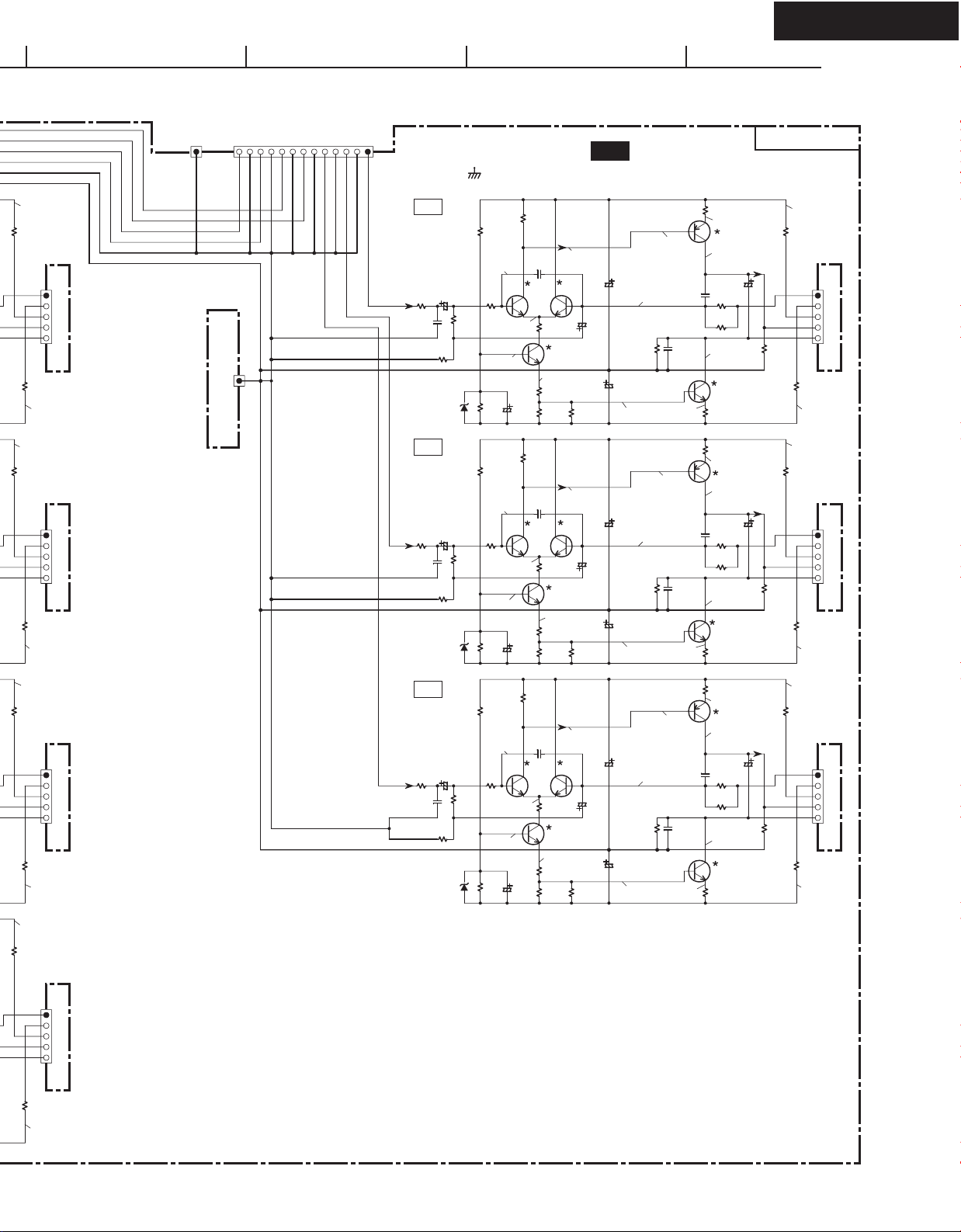
NC
NC
53.0V
R5183
10
(1/4W)
P6003A
NF
-B1
+B1
B+
B-
R5193
10
(1/4W)
53.0V
R5184
10
(1/4W)
P6004A
NF
-B1
+B1
B+
B-
(1/4W)
TO NAAF-8523
-53.0V
TO NAAF-8523
R5194
10
-53.0V
TO NAAF-8523
P5503A
E
TO NAAF-8523
TO NAAF-8523
SBR
SBL
(BUS-BAR)
P6011B
P5504A
L
C
SR
R
SL
R5000
1K
C5000
101K
R5040
D5000
MTZJ5.6B
DZ-5.6BSB
R5001
1K
C5001
101K
R5041
D5001
MTZJ5.6B
DZ-5.6BSB
P5019
L
C5010
47/50
R5010
56K
2.2K
R
C5011
47/50
R5011
56K
2.2K
R5090
100K
-0.1V
R5020
330
-47.5V
R5100
100K
R5091
100K
-0.1V
R5021
330
-47.5V
R5101
100K
-0.65V
C5020
10/50
-0.65V
C5021
10/50
R5110
1K
C5030
NC
Q5000
R5111
1K
C5031
NC
Q5001
R5050
4.7K
Q5050
-48.1V
R5060
1.2K
R5070
NC
R5051
4.7K
Q5051
-48.1V
R5061
1.2K
R5071
NC
U22
DRIVER AMPLIIER PC BOARD
R5160
100
(1/4W)
52.5V
Q5010
Q5011
51.5V
R5080
470
51.5V
R5081
C5040
220/25
C5041
220/25
470
C5100
10/100
C5110
10/100
C5101
10/100
C5111
10/100
-51.7V
R5130
22K
-51.7V
R5131
22K
52.0V
[65.1V]
0V
-52.2V
100
52.0V
0V
-52.2V
C5080
040C
C5090
101K
R5161
(1/4W)
C5081
040C
C5091
101K
R5230
R5231
1.1V
R5030
120K
-1.1V
R5170
100
(1/4W)
52.5V
1.1V
R5031
120K
-1.1V
R5171
100
(1/4W)
Q5030
C5050
47/50
120K
Q5040
Q5031
C5051
47/50
120K
Q5041
R5200
22K
R5201
22K
53.0V
R5180
10
(1/4W)
P6000A
NF
-B1
+B1
B+
B-
R5190
(1/4W)
-53.0V
53.0V
R5181
10
(1/4W)
P6001A
NF
-B1
+B1
B+
B-
R5191
(1/4W)
-53.0V
TO NAAF-8523
10
TO NAAF-8523
10
NAAF-8540
NC
NC
53.0V
R5185
10
(1/4W)
P6005A
NF
-B1
+B1
B+
B-
R5195
10
(1/4W)
-53.0V
53.0V
R5186
10
(1/4W)
JL6006A
NF
-B1
+B1
B+
B-
R5196
10
(1/4W)
-53.0V
TO NAAF-8523
TO NAAF-8523
C
R5002
1K
C5002
101K
R5042
D5002
MTZJ5.6B
DZ-5.6BSB
C5012
10/50
2.2K
R5012
56K
R5092
100K
-0.1V
R5022
330
-47.5V
R5102
100K
R5112
1K
C5032
NC
Q5002 Q5012
-0.65V
C5022
10/50
R5052
4.7K
Q5052
-48.1V
R5062
1.2K
R5072
NC
51.5V
R5082
470
C5042
220/25
C5102
10/100
C5112
10/100
-51.7V
R5132
18K
R5162
100
(1/4W)
52.5V
C5082
040C
C5092
101K
R5232
1.1V
R5032
120K
-1.1V
R5172
100
(1/4W)
Q5032
C5052
47/50
120K
Q5042
52.0V
0V
-52.2V
R5202
NC
53.0V
R5182
10
(1/4W)
P6002A
NF
-B1
+B1
B+
B-
(1/4W)
-53.0V
TO NAAF-8523
R5192
10

TX-SR603/603E/8360
A
SCHEMATIC DIAGRAMS-3
POWER AMPLIFIER SECTION-1
1
Refer to following table about the parts displayed by mark " ".
Transistors
CIRCUIT NO.
Q5000 - 5002
Q5010 - 5012
Q5003 - 5006
Q5013 - 5016
Q5030 -5036
Q5040 - 5046
Q5050 - 5056
NOTE
2
THE COMPONENTS IDENTIFIED BY MARK ARE CRITICAL FOR SAFETY
REPLACE ONLY WITH PART NUMBER SPECIFIED.
VOLTAGE (MEASURED WITH VOLTMETER) IS DC VOLTAGE.(NO INPUT SIGNAL).
ALL PNP TRANSISTORS ARE EQUIVALENT TO 2SA1015-GR UNLESS OTHERWISE NOTED.
ALL NPN TRANSISTORS ARE EQUIVALENT TO 2SC1815-GR UNLESS OTHERWISE NOTED.
ALL DIODES ARE EQUIVALENT TO 1SS133 UNLESS OTHERWISE NOTED.
ELECTROLYTIC CAPACITORS ( ) ARE IN uF/WV.
ALL CAPACITORS ARE IN pF/50WV UNLESS OTHERWISE NOTED.
EX) 030- 3pF 330- 33pF 331- 330pF 333- 0.033uF
ALL RESISTORS ARE IN OHMS 1/4WATTS UNLESS OTHERWISE NOTED.
THE THICK LINES ON PC BOARD ARE THE PRINTING SIDE OF THE PARTS.
EX) PRINTING SIDE
CIRCUIT IS SUBJECT TO CHANGE FOR IMPROVEMENT.
<Note>
NC=No mount of parts.
3
DESCRIPTION
2SC2240-BL
2SC2240-BL, KTC3200-BL
2SA949-Y
2SC2229-Y
2SC2240-GR, BL
!
BCDEFGH
TO NAAF-8523
SBR
SBL
(BUS-BAR)
P6011B
P5504A
L
C
SR
R
SL
R5000
1K
C5000
101K
R5040
D5000
MTZJ5.6B
DZ-5.6BSB
R5001
1K
C5001
101K
R5041
D5001
MTZJ5.6B
DZ-5.6BSB
P5019
L
C5010
47/50
R5010
56K
2.2K
R
C5011
47/50
R5011
56K
2.2K
R5090
100K
-0.1V
R5020
330
-47.5V
R5100
100K
R5091
100K
-0.1V
R5021
330
-47.5V
R5101
100K
-0.65V
C5020
10/50
-0.65V
C5021
10/50
R5110
1K
C5030
NC
Q5000
R5111
1K
C5031
NC
Q5001
R5050
4.7K
Q5050
-48.1V
R5060
1.2K
R5070
NC
R5051
4.7K
Q5051
-48.1V
R5061
1.2K
R5071
NC
U22
DRIVER AMPLIIER PC BOARD
R5160
100
(1/4W)
52.5V
Q5010
Q5011
51.5V
R5080
470
51.5V
R5081
C5040
220/25
C5041
220/25
470
C5100
10/100
C5110
10/100
C5101
10/100
C5111
10/100
-51.7V
R5130
22K
-51.7V
R5131
22K
52.0V
[65.1V]
0V
-52.2V
100
52.0V
0V
-52.2V
C5080
040C
C5090
101K
R5161
(1/4W)
C5081
040C
C5091
101K
R5230
R5231
1.1V
R5030
120K
-1.1V
R5170
100
(1/4W)
52.5V
1.1V
R5031
120K
-1.1V
Q5041
R5171
100
(1/4W)
Q5030
C5050
47/50
120K
Q5040
Q5031
C5051
47/50
120K
R5200
22K
R5201
22K
53.0V
R5180
10
(1/4W)
P6000A
NF
-B1
+B1
B+
B-
R5190
10
(1/4W)
-53.0V
53.0V
R5181
10
(1/4W)
P6001A
NF
-B1
+B1
B+
B-
R5191
10
(1/4W)
-53.0V
TO NAAF-8523
TO NAAF-8523
NAAF-8540
SL
R5003
1K
C5003
101K
R5043
D5003
MTZJ5.6B
DZ-5.6BSB
SR
R5004
1K
C5004
101K
R5044 2.2K
D5004
MTZJ5.6B
DZ-5.6BSB
C5013
10/50
2.2K
C5014
10/50
R5013
56K
R5014
56K
R5093
100K
-0.1V
R5023
330
-47.5V
R5103
100K
R5094
100K
-0.1V
R5024
330
-47.5V
R5104
100K
R5113
1K
C5033
Q5003 Q5013
-0.65V
C5023
10/50
R5114
C5034
Q5004 Q5014
-0.65V
C5024
10/50
TO NAAF-8523
P5503A
E
R5203
NC
R5204
NC
53.0V
R5183
10
(1/4W)
P6003A
NF
-B1
+B1
B+
B-
R5193
10
(1/4W)
53.0V
R5184
10
(1/4W)
P6004A
NF
-B1
+B1
B+
B-
(1/4W)
TO NAAF-8523
-53.0V
TO NAAF-8523
R5194
10
-53.0V
TO NAAF-8523
R5163
100
(1/4W)
52.5V
C5083
040C
C5093
101K
(1/4W)
C5084
040C
C5094
101K
R5233
R5234
1.1V
R5033
120K
-1.1V
Q5043
R5173
100
(1/4W)
52.5V
1.1V
R5034
120K
-1.1V
R5174
100
(1/4W)
Q5033
C5053
47/50
120K
Q5034
C5054
47/50
120K
Q5044
52.0V
51.5V
NC
R5053
4.7K
Q5053
-48.1V
R5063
1.2K
R5073
NC
1K
NC
R5054
4.7K
Q5054
-48.1V
R5064
1.2K
R5074
NC
R5083
470
51.5V
R5084
470
C5043
220/25
C5044
220/25
C5103
10/100
C5113
10/100
-51.7V
C5104
10/100
C5114
10/100
R5133
18K
0V
R5134
18K
-51.7V
0V
-52.2V
R5164
100
52.0V
-52.2V
18K
18K
R5165
(1/4W)
100
52.0V
0V
100
52.0V
0V
C5085
040C
C5095
101K
-52.2V
R5166
(1/4W)
C5086
040C
C5096
101K
-52.2V
R5235
R5236
52.5V
1.1V
R5035
120K
-1.1V
R5175
100
(1/4W)
52.5V
1.1V
R5036
120K
-1.1V
R5176
100
(1/4W)
Q5035
C5055
47/50
120K
Q5045
Q5036
C5056
47/50
120K
Q5046
SBL
C5015
R5005
10/50
1K
R5015
2.2K
56K
R5025
R5105
C5005
101K
4
R5045
D5005
MTZJ5.6B
DZ-5.6BSB
SBR
C5016
R5006
10/50
1K
R5016
C5006
101K
56K
R5026
5
2.2K
R5046
D5006
MTZJ5.6B
DZ-5.6BSB
R5106
R5095
100K
-0.1V
330
-47.5V
100K
R5096
100K
-0.1V
330
-47.5V
100K
C5035
Q5005
-0.65V
C5025
10/50
R5116
1K
C5036
Q5006 Q5016
-0.65V
C5026
10/50
R5115
1K
NC
NC
R5055
4.7K
Q5055
-48.1V
R5065
1.2K
R5075
NC
R5056
4.7K
Q5056
-48.1V
R5066
1.2K
R5076
NC
Q5015
51.5V
R5085
51.5V
R5086
C5045
220/25
470
C5046
220/25
470
C5105
10/100
R5135
C5115
10/100
-51.7V
C5106
10/100
C5116
10/100
-51.7V
R5136
R5205
NC
R5206
NC
53.0V
R5185
10
(1/4W)
P6005A
NF
-B1
+B1
B+
B-
R5195
10
(1/4W)
-53.0V
53.0V
R5186
10
(1/4W)
JL6006A
NF
-B1
+B1
B+
B-
R5196
10
(1/4W)
-53.0V
TO NAAF-8523
TO NAAF-8523
C
R5002
1K
C5002
101K
R5042
D5002
MTZJ5.6B
DZ-5.6BSB
C5012
10/50
2.2K
R5012
56K
R5092
100K
-0.1V
R5022
330
-47.5V
R5102
100K
R5112
1K
C5032
NC
Q5002 Q5012
-0.65V
C5022
10/50
R5052
4.7K
Q5052
-48.1V
R5062
1.2K
R5072
NC
51.5V
R5082
470
C5042
220/25
C5102
10/100
C5112
10/100
-51.7V
R5132
18K
R5162
100
(1/4W)
52.5V
C5082
040C
C5092
101K
R5232
Q5032
1.1V
R5032
120K
-1.1V
Q5042
R5172
100
(1/4W)
C5052
47/50
120K
52.0V
0V
-52.2V
R5202
NC
53.0V
R5182
10
(1/4W)
P6002A
NF
-B1
+B1
B+
B-
(1/4W)
-53.0V
TO NAAF-8523
R5192
10
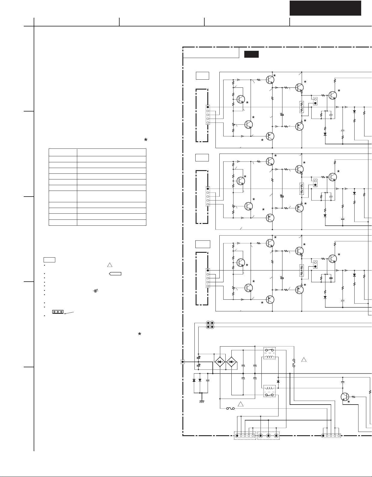
TX-SR603/603E/8360 TX-SR603/603E/8360
A
SCHEMATIC DIAGRAMS-4
POWER AMPLIFIER SECTION-2
1
Refer to following table about the parts displayed by mark " ".
Transistors
2
CIRCUIT NO.
Q6010 - 6016
Q6020 - 6026 2SC1740S-S
Q6030 - 6036 2SC5171, 2SC5993-Q, P
Q6040 - 6046 2SA1930, 2SA2140-Q, P
Q6070 - 6076
Q6701, 6702 2SC2240-GR, BL, KTC3200-GR, BL
Q6703 KTA1268-BL, GR, 2SA992-E, F
Q6050 - 6052
Q6053 - 6055
Q6060 - 6062
Q6063 - 6060
DESCRIPTION
2SC1740S-S
2SC2229-Y
2SA1123-R
2SC5242-O, R
2SC5242-O, R, MN130S-Y, P, O
2SA1962-O, R
2SA1962-O,R, MP130S-Y, P, O
BCDEFGH
NAAF-8523(2/2)
SL
TO NAAF-8540
SR
TO NAAF-8540/8550
P6003B
NF
-B1
+B1
B+
B-
P6004B
NF
-B1
+B1
B+
B-
R6033
470
R6003
5.6K
R6013
3.9K
R6043
2K
R6053
3.3K
R6034
470
R6004
5.6K
R6014
3.9K
R6044
2K
R6054
3.3K
U05
AMPLIFIER PC BOARD
1.0V
IDLING
ADJ.
-0.4V
1.0V
IDLING
ADJ.
-0.4V
-0.3V
-53.0V
-0.3V
-53.0V
R6023 2.2
(1/4W)
1.1V
Q6013
Q6023
-1.1V
R6024 2.2
(1/4W)
1.1V
Q6014
Q6024
-1.1V
0.6V
-0.6V
Q6043
0.6V
-0.6V
Q6044
Q6033
R6073
120
(1/4W)
C6043
47/50
Q6034
R6074
120
(1/4W)
C6044
47/50
R6083
0.22
(1/4W)
R6093
0.22
(1/4W)
R6084
0.22
(1/4W)
R6094
0.22
(1/4W)
0.6V
R6103
0.22x2
-0.6V
0.6V
R6104
0.22x2
-0.6V
53.0V
(5W)
53.0V
(5W)
Q6053
Q6063
Q6054
Q6064
P6083
R6153
P6084
R6154
12K
12K
R6143
22K
ID+
ID-
R6144
22K
ID+
ID-
R6163
D6013
R6164
D6014
33K
C6053
NC
R6193
220K
33K
C6054
NC
R6194
220K
Q6073
Q6074
R6183
47K
C6233
473J
R6233
8.2 (1W)
R6184
47K
R6234
8.2(1W)
C6234
473J
D6003
D6004
R6174
47K
R6173
47K
3
NOTE
THE COMPONENTS IDENTIFIED BY MARK ARE CRITICAL FOR SAFETY
REPLACE ONLY WITH PART NUMBER SPECIFIED.
VOLTAGE (MEASURED WITH VOLTMETER) IS DC VOLTAGE.(NO INPUT SIGNAL).
ALL PNP TRANSISTORS ARE EQUIVALENT TO 2SA1015-GR UNLESS OTHERWISE NOTED.
ALL NPN TRANSISTORS ARE EQUIVALENT TO 2SC1815-GR UNLESS OTHERWISE NOTED.
ALL DIODES ARE EQUIVALENT TO 1SS133 UNLESS OTHERWISE NOTED.
ELECTROLYTIC CAPACITORS ( ) ARE IN uF/WV.
ALL CAPACITORS ARE IN pF/50WV UNLESS OTHERWISE NOTED.
EX) 030- 3pF 330- 33pF 331- 330pF 333- 0.033uF
ALL RESISTORS ARE IN OHMS 1/4WATTS UNLESS OTHERWISE NOTED.
THE THICK LINES ON PC BOARD ARE THE PRINTING SIDE OF THE PARTS.
EX) PRINTING SIDE
CIRCUIT IS SUBJECT TO CHANGE FOR IMPROVEMENT.
<Note>
4
NC=No mount of parts.
Refer to following table about the parts displayed by mark " ".
5
R6025 2.2
-0.4V
-0.3V
-53.0V
C6905
C6904
!
Q6015
334J 100V
334J 100V
(1/4W)
1.1V
Q6025
-1.1V
C6907
C6906
104J
104J
0.6V
-0.6V
Q6045
RL6902
D6906
RL6901
P6005B
NF
-B1
+B1
B+
B-
J011A
D6905
C6903
104J
J010A
R6035
470
R6005
5.6K
R6015
3.9K
R6045
2K
R6055
3.3K
D6904
F6901
12A/250V
NC
JL6951A
1.0V
IDLING
ADJ.
SBL
!
TO NAAF-8540
J011
J010
P6011A
(BUS BAR)
C6901
10000/63
C6902
10000/63
TO NAAF-8540
D6902
D6901
P6906
D6901,6902
RL1N40003
GP104003E
TO NAPS-8524
Q6035
R6075
220
(1/4W)
C6045
47/50
R6085
0.22
(1/4W)
R6095
0.22
(1/4W)
0.6V
-0.6V
P995
P996
P997
53.0V
R6105
0.22x2
(5W)
Q6055
Q6065
!
F6902
12A/250V
P6085
R6165
33K
R6145
22K
ID+
ID-
R6155
12K
C6055
NC
R6195
220K
D6015
TO NAPS-8524
Q6075
JL6952A
R6185
47K
R6235
8.2(1W)
C6235
473J
C6920
NC
D6005
R6902
1K
Q6901
R6175
47K
(1/2W)

R6173
47K
L
TO NAAF-8540
P6000B
NF
-B1
+B1
B+
B-
R6030
R6000
R6010
R6040
R6050
470
5.6K
3.9K
3.3K
R6020 2.2
(1/4W)
1.1V
1.0V
0.6V
-0.6V
Q6040
R6070
(1/4W)
C6040
Q6010
-0.3V
IDLING
Q6020
ADJ.
2K
-0.4V
-1.1V
-53.0V
Q6030
82
47/50
R6080
0.22
(1/4W)
R6090
0.22
(1/4W)
53.0V
0.6V
R6100
0.22x2
(5W)
-0.6V
Q6050
Q6060
P6080
R6150
12K
R6140
22K
ID+
ID-
D6010
R6160
33K
C6050
NC
R6190
220K
Q6070
R6180
47K
R6230
8.2(1W)
C6230
473J
D6000
R6170
47K
R6901
10
(1/2W)
R
TO NAAF-8540
C
TO NAAF-8540
P6001B
NF
-B1
+B1
B+
B-
P6002B
NF
-B1
+B1
B+
B-
R6031
R6001
R6011
R6041
R6051
R6032
R6002
R6012
R6042
R6052
5.6K
3.9K
3.3K
470
5.6K
3.9K
3.3K
470
2K
2K
1.0V
IDLING
ADJ.
-0.4V
1.0V
IDLING
ADJ.
-0.4V
-0.3V
-53.0V
-0.3V
-53.0V
R6021 2.2
(1/4W)
1.1V
Q6011
Q6021
-1.1V
R6022 2.2
(1/4W)
1.1V
Q6012
Q6022
-1.1V
0.6V
-0.6V
Q6041
-0.6V
Q6042
0.6V
Q6031
R6071
(1/4W)
C6041
47/50
Q6032
R6072
82
(1/4W)
C6042
47/50
R6701
22K
D6701
C6701
100/16
82
R6702
10K
R6708
R6081
0.22
(1/4W)
R6091
0.22
(1/4W)
R6082
0.22
(1/4W)
R6092
0.22
(1/4W)
33K
0.6V
R6101
0.22x2
(5W)
-0.6V
0.6V
R6102
0.22x2
(5W)
-0.6V
C6703
223Z
Q6702Q6701
C6704
1/100
D6702
53.0V
53.0V
[66.5V]
Q6051
P6081
Q6061
Q6052
P6082
Q6062
Q6703
R6704
47K
D6703
MTZJ5.1B
DZ5.1BSB
R6706
220K
R6151
12K
R6152
12K
C6706
100/16
R6141
22K
ID+
ID-
R6142
22K
ID+
ID-
R6161
33K
C6051
NC
R6191
220K
D6011
R6162
33K
C6052
NC
R6192
220K
D6012
D6704
MTZJ5.1B
DZ5.1BSB
Q6071
Q6072
5.6K
R6709
R6181
47K
C6231
473J
R6231
8.2
R6182
47K
R6232
8.2
C6232
473J
R6710
(1W)
(1W)
12K
D6001
D6002
R6171
47K
R6172
47K
R6176
47K
R6236
C6236
473J
R6186
47K
R6751
390
(1/2W)
U12
(1W)
8.2
D6006
R6750
390
(1/2W)
NAETC-8526
THERMAL SENSOR
PC BOARD
Q6380
LM61CIZ
GOV
C6380
NC
JL6402B
JL6402A
HPDET
+24V
SEC1H
RLGND
MPUGND
VOLH
PRO
THRM
JL6200A
+B1
-B1
E
SBRSP
IPRO
SBRSP
SBLSP
SRSP
SLSP
CSP
RSP
LSP
JL6600A
SRSPE
SLSPE
SBRSPE
SBLSPE
CSPE
RSPE
LSPE
RLGND
+24V
JL6803A
HPL
HPR
JL891B
THERMAL SENSOR
C6381
NC
5V
TO NAETC-8525
TO NAETC
-8537
TO NAETC
-8537
TO NAETC
-8516
TO NAAF-8523
(1/2)
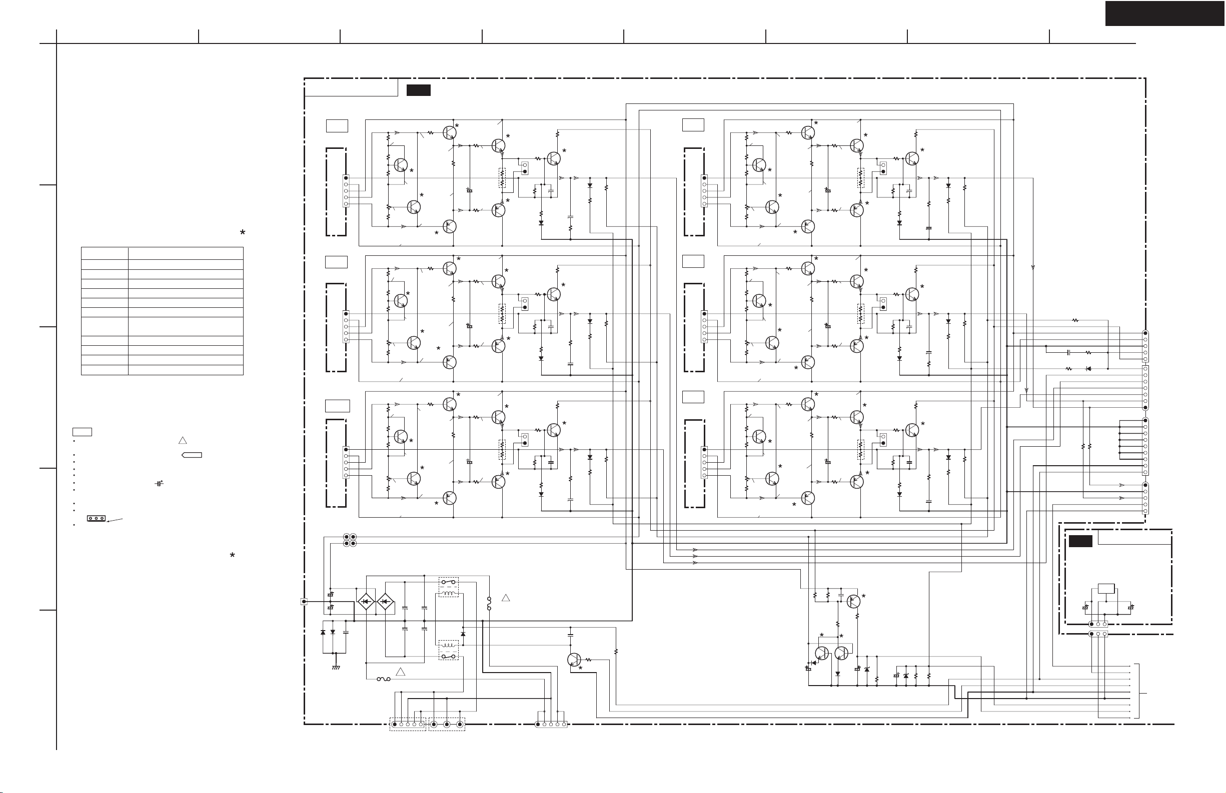
TX-SR603/603E/8360
A
SCHEMATIC DIAGRAMS-4
POWER AMPLIFIER SECTION-2
1
Refer to following table about the parts displayed by mark " ".
Transistors
2
CIRCUIT NO.
Q6010 - 6016
Q6020 - 6026 2SC1740S-S
Q6030 - 6036 2SC5171, 2SC5993-Q, P
Q6040 - 6046 2SA1930, 2SA2140-Q, P
Q6070 - 6076
Q6701, 6702 2SC2240-GR, BL, KTC3200-GR, BL
Q6703 KTA1268-BL, GR, 2SA992-E, F
Q6050 - 6052
Q6053 - 6055
Q6060 - 6062
Q6063 - 6060
3
NOTE
THE COMPONENTS IDENTIFIED BY MARK ARE CRITICAL FOR SAFETY
REPLACE ONLY WITH PART NUMBER SPECIFIED.
VOLTAGE (MEASURED WITH VOLTMETER) IS DC VOLTAGE.(NO INPUT SIGNAL).
ALL PNP TRANSISTORS ARE EQUIVALENT TO 2SA1015-GR UNLESS OTHERWISE NOTED.
ALL NPN TRANSISTORS ARE EQUIVALENT TO 2SC1815-GR UNLESS OTHERWISE NOTED.
ALL DIODES ARE EQUIVALENT TO 1SS133 UNLESS OTHERWISE NOTED.
ELECTROLYTIC CAPACITORS ( ) ARE IN uF/WV.
ALL CAPACITORS ARE IN pF/50WV UNLESS OTHERWISE NOTED.
EX) 030- 3pF 330- 33pF 331- 330pF 333- 0.033uF
ALL RESISTORS ARE IN OHMS 1/4WATTS UNLESS OTHERWISE NOTED.
THE THICK LINES ON PC BOARD ARE THE PRINTING SIDE OF THE PARTS.
EX) PRINTING SIDE
CIRCUIT IS SUBJECT TO CHANGE FOR IMPROVEMENT.
<Note>
4
NC=No mount of parts.
Refer to following table about the parts displayed by mark " ".
5
DESCRIPTION
2SC1740S-S
2SC2229-Y
2SA1123-R
2SC5242-O, R
2SC5242-O, R, MN130S-Y, P, O
2SA1962-O, R
2SA1962-O,R, MP130S-Y, P, O
!
BCDEFGH
NAAF-8523(2/2)
SL
P6003B
NF
-B1
+B1
B+
B-
TO NAAF-8540
SR
NF
-B1
+B1
B+
B-
TO NAAF-8540/8550
SBL
NF
-B1
+B1
B+
B-
TO NAAF-8540
J011
J011A
J010
(BUS BAR)
C6901
10000/63
C6902
10000/63
D6902
P6906
D6901,6902
RL1N40003
GP104003E
D6901
D6905
C6903
104J
P6011A
TO NAAF-8540
P6004B
P6005B
J010A
R6033
470
R6003
5.6K
R6013
3.9K
R6043
2K
R6053
3.3K
R6034
470
R6004
5.6K
R6014
3.9K
R6044
2K
R6054
3.3K
R6035
470
R6005
5.6K
R6015
3.9K
R6045
2K
R6055
3.3K
D6904
F6901
12A/250V
NC
JL6951A
U05
AMPLIFIER PC BOARD
1.0V
IDLING
ADJ.
-0.4V
1.0V
IDLING
ADJ.
-0.4V
1.0V
IDLING
ADJ.
-0.4V
!
-0.3V
-53.0V
-0.3V
-53.0V
-0.3V
-53.0V
C6905
C6904
R6023 2.2
(1/4W)
1.1V
Q6013
Q6023
-1.1V
R6024 2.2
1.1V
Q6014
Q6024
-1.1V
R6025 2.2
(1/4W)
1.1V
Q6015
Q6025
-1.1V
C6907
334J 100V
C6906
334J 100V
(1/4W)
Q6033
R6083
0.22
(1/4W)
0.6V
R6073
120
(1/4W)
C6043
-0.6V
47/50
R6093
0.22
(1/4W)
Q6043
Q6034
R6084
0.22
(1/4W)
0.6V
R6074
120
(1/4W)
-0.6V
C6044
47/50
0.6V
-0.6V
RL6902
D6906
RL6901
Q6035
R6075
220
(1/4W)
C6045
47/50
R6094
0.22
(1/4W)
R6085
0.22
(1/4W)
R6095
0.22
(1/4W)
P995
P996
P997
Q6044
Q6045
104J
104J
TO NAPS-8524
0.6V
R6103
0.22x2
(5W)
-0.6V
0.6V
R6104
0.22x2
(5W)
-0.6V
53.0V
0.6V
R6105
0.22x2
(5W)
-0.6V
53.0V
53.0V
Q6053
Q6063
Q6054
Q6064
Q6055
Q6065
!
F6902
12A/250V
P6085
R6163
33K
R6143
22K
P6083
ID+
ID-
R6153
12K
C6053
NC
R6193
220K
D6013
R6164
33K
R6144
22K
P6084
ID+
ID-
R6154
12K
C6054
NC
R6194
220K
D6014
R6165
33K
R6145
22K
ID+
ID-
R6155
12K
C6055
NC
R6195
220K
D6015
TO NAPS-8524
Q6073
Q6074
Q6075
JL6952A
R6183
47K
C6233
473J
R6233
8.2 (1W)
R6184
47K
R6234
8.2(1W)
C6234
473J
R6185
47K
R6235
8.2(1W)
C6235
473J
C6920
NC
D6003
D6004
D6005
R6902
1K
Q6901
R6174
47K
R6175
47K
R6173
47K
R6901
10
(1/2W)
L
TO NAAF-8540
P6000B
NF
-B1
+B1
B+
B-
R6030
R6000
R6010
R6040
R6050
R
R6001
P6001B
R6011
NF
-B1
+B1
B+
B-
TO NAAF-8540
C
TO NAAF-8540
P6002B
NF
-B1
+B1
B+
B-
R6051
R6032
R6012
R6042
R6052
470
5.6K
3.9K
2K
3.3K
R6031
470
5.6K
3.9K
R6041
2K
3.3K
470
R6002
5.6K
3.9K
2K
3.3K
1.0V
IDLING
ADJ.
-0.4V
1.0V
IDLING
ADJ.
-0.4V
1.0V
IDLING
ADJ.
-0.4V
-0.3V
-53.0V
-0.3V
-53.0V
-0.3V
-53.0V
R6020 2.2
(1/4W)
1.1V
Q6010
Q6020
-1.1V
R6021 2.2
(1/4W)
1.1V
Q6011
Q6021
-1.1V
R6022 2.2
(1/4W)
1.1V
Q6012
Q6022
-1.1V
0.6V
-0.6V
Q6040
0.6V
-0.6V
Q6041
-0.6V
Q6042
0.6V
Q6030
R6070
82
(1/4W)
C6040
47/50
Q6031
R6071
82
(1/4W)
C6041
47/50
Q6032
R6072
82
(1/4W)
C6042
47/50
R6701
22K
D6701
C6701
100/16
(1/4W)
(1/4W)
R6702
10K
R6708
33K
R6080
0.22
R6090
0.22
(1/4W)
R6081
0.22
(1/4W)
R6091
0.22
(1/4W)
R6082
0.22
R6092
0.22
(1/4W)
53.0V
0.6V
R6100
0.22x2
(5W)
-0.6V
53.0V
0.6V
R6101
0.22x2
(5W)
-0.6V
53.0V
[66.5V]
0.6V
R6102
0.22x2
(5W)
-0.6V
C6703
223Z
Q6702Q6701
C6704
1/100
D6702
Q6050
P6080
Q6060
Q6051
P6081
Q6061
Q6052
P6082
Q6062
Q6703
R6704
47K
D6703
MTZJ5.1B
DZ5.1BSB
R6706
220K
R6150
12K
R6151
12K
R6152
12K
C6706
100/16
R6140
22K
ID+
ID-
R6141
22K
ID+
ID-
R6142
22K
ID+
ID-
R6160
33K
C6050
NC
R6190
220K
D6010
R6161
33K
C6051
NC
R6191
220K
D6011
R6162
33K
C6052
NC
R6192
220K
D6012
D6704
MTZJ5.1B
DZ5.1BSB
Q6070
Q6071
Q6072
5.6K
R6709
R6180
47K
R6230
8.2(1W)
C6230
473J
R6181
47K
C6231
473J
R6231
(1W)
8.2
R6182
47K
R6232
(1W)
8.2
C6232
473J
R6710
D6000
D6001
D6002
12K
R6171
47K
R6172
47K
R6170
47K
R6176
47K
473J
47K
R6751
390
(1/2W)
U12
R6236
(1W)
8.2
D6006
R6750
390
(1/2W)
NAETC-8526
C6236
R6186
THERMAL SENSOR
PC BOARD
Q6380
LM61CIZ
GOV
C6380
NC
JL6402B
JL6402A
HPDET
+24V
SEC1H
RLGND
MPUGND
VOLH
PRO
THRM
JL6200A
+B1
-B1
E
SBRSP
IPRO
SBRSP
SBLSP
SRSP
SLSP
CSP
RSP
LSP
JL6600A
SRSPE
SLSPE
SBRSPE
SBLSPE
CSPE
RSPE
LSPE
RLGND
+24V
JL6803A
HPL
HPR
JL891B
THERMAL SENSOR
C6381
NC
5V
TO NAETC-8525
TO NAETC
-8537
TO NAETC
-8537
TO NAETC
-8516
TO NAAF-8523
(1/2)

TX-SR603/603E/8360
A
SCHEMATIC DIAGRAMS-5
SPEAKER TERMINAL SECTION
NAETC-8538
1
2
3
4
U20
CENTER SPEAKER
TERMINALPC BOARD
TO NAVD-8476
BCD
L6602 S1.3C
R6602 22
CSP
CSRLD
R6612 22
J6603
JL6602A
JL6602B
CSPE
RL6600
C6600
103J
D6603
RL6603
C6605 103Z
RL6605
C6607
103Z
RL6607
NC
D6600
C6603
D6605
D6607
103Z
C6642
U19
SPEAKER TERMINAL
PC BOARD
C6640 103J
C6641 103J
FRONT SPEAKERS
L
R
SURROUND SPEAKERS
L
R
P6600
C6643
C6644 103J
C6645 103J
C6646 103J
SURROUND BACK
SPEAKERS
P6605
L
R
ZONE 2 SPEAKERS
P6607
L
R
C6647 103J
C6648 103J
R6690 10
(1/2W)
RL6602
C6602
103J
+24VR
S1.3C
L6600
R6600 22
R6610 22
J6600
NC
L6601
S1.3C
R6601 22
22
R6611
J6604
NC
L6603
S1.3C
R6603
22
22
R6613
J6619
NC
L6604
JL6600B
LSP
RSP
CSP LSPE
SLSP RSPE
SRSP CSPE
SBLSP SLSPE
SBRSP SRSPE
TO NAAF-8523
JL2006B
RLGND
Z2RLD
SBRLD
CSRLD
FRLD
S1.3C
R6604
22
22
R6614
J6620
NC
L6605
S1.3C
R6605 22
R6615
22
J6626
NC
L6606 S1.3C
R6606
22
22
R6616
J6625
NC
CENTER SPEAKER
P6602
103J
NAETC-8537
103J
C6652
102J
C6655
102J
C6656
102J
C6657
102J
C6658
102J
C6650
102J
C6651
102J
C6653
102J
C6654
102J
SBLSPE
SBRSPE
RLGND
+24V
JL6603B
TO NAAF-8523
Refer to following table about the parts displayed
by mark " ".
Transistors
CIRCUIT NO.
Q6016
DESCRIPTION
2SC1740S-S
Q6026 2SC1740S-S
Q6036 2SC5171,
Q6046 2SA1930,
5
Q6076
Q6056 2SC5242-O, R,
Q6066 2SA1962-O,R,
2SC5993-Q, -P
2SA2140-Q, -P
2SC2229-Y
MN130S-Y, P, O
MP130S-Y, P, O
U11
SBR AMPLIFIER PC BOARD
SBR
JL6006B
NF
-B1
+B1
B+
B-
TO NAAF-8540
R6036
470
R6006
5.6K
R6016
3.9K
R6046
2K
R6056
3.3K
1.0V
Q6016
IDLING
ADJ.
-0.4V
-0.3V
-53.0V
R6026 2.2
(1/4W)
1.1V
Q6026
-1.1V
-0.6V
Q6046
0.6V
Q6036
R6076
220
(1/4W)
C6046
47/50
R6086
0.22
(1/4W)
R6096
0.22
(1/4W)
0.6V
R6106
0.22x2
(5W)
-0.6V
53.0V
Q6056
Q6066
P6086
R6156
12K
R6146
22K
ID+
ID-
R6166
D6016
33K
C6056
NC
R6196
220K
NAETC-8525
R6516
NC
Q6076
C6516
NC
C6526
NC
R6526
NC
JL6200B
+B1
-B1
E
SBRSP
IPRO
TO NAAF-8523
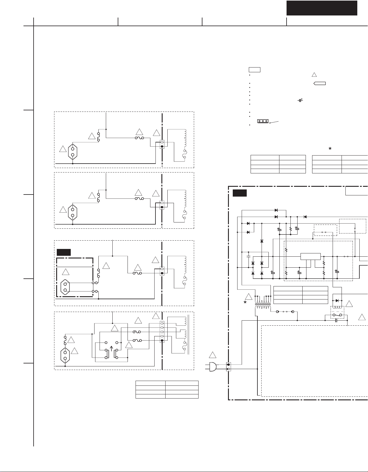
TX-SR603/603E/8360 TX-SR603/603E/8360
A
SCHEMATIC DIAGRAMS-6
POWER SUPPLY SECTION
1
MPP, MPA
F903
T2.5AL250V
!
P902
!
!
!
P902A
AC OUTLET
100W MAX
P902
AC OUTLET
100W MAX
OUTLET
PC BOARD
P926A
P925A
!
!
P902
AC OUTLET
100W MAX
F903
T2.5AL250V
!
!
F903
T2.5AL250V
P926
P925
S902
VOLTAGE
SELECTOR
220V
120V
!
2
MGR, MGQ
3
MGK
U16
NAPS-8534
AC OUTLET 100W MAX
4
MWT
F903
T2.5AL250V
T5AL/250V
F902
T5AL/250V
F902
T5AL/250V
F902
T5AL/250V
F901
!
10A/125V
F902
!
!
!
BCDEFGH
NOTE
THE COMPONENTS IDENTIFIED BY MARK ARE CRITICAL FOR SAFETY
REPLACE ONLY WITH PART NUMBER SPECIFIED.
VOLTAGE (MEASURED WITH VOLTMETER) IS DC VOLTAGE.(NO INPUT SIGNAL).
ALL PNP TRANSISTORS ARE EQUIVALENT TO 2SA1015-GR UNLESS OTHERWISE NOTED.
ALL NPN TRANSISTORS ARE EQUIVALENT TO 2SC1815-GR UNLESS OTHERWISE NOTED.
ALL DIODES ARE EQUIVALENT TO 1SS133 UNLESS OTHERWISE NOTED.
ELECTROLYTIC CAPACITORS ( ) ARE IN uF/WV.
ALL CAPACITORS ARE IN pF/50WV UNLESS OTHERWISE NOTED.
EX) 030- 3pF 330- 33pF 331- 330pF 333- 0.033uF
ALL RESISTORS ARE IN OHMS 1/4WATTS UNLESS OTHERWISE NOTED.
THE THICK LINES ON PC BOARD ARE THE PRINTING SIDE OF THE PARTS.
T901
!
!
P912
T901
P912
!
T901
U15
POWER SUPPLY-1 PC BOARD
!
P912
T901
!
P901
AC-H
AC-G
P901A
P912
!
EX) PRINTING SIDE
CIRCUIT IS SUBJECT TO CHANGE FOR IMPROVEMENT.
<Note>
NC=No mount of parts.
Refer to following table about the parts displayed by mark " ".
T902
DESTINATION
MPP, MPA
MGR, MGQ, MGK
MWT
D930
D931
D932
C921
223Z
!
T902
D921
D923
4
D935
D933
C930
100/35
D922
D924
C922
C922
DESTINATION
MPP, MPA
MGR, MGQ, MGK
MWT
1
3
DESCRIPTION
NPT-1520GQ
NPT-1520GQ
NPT-1520JQ
R934
100K
MWT only
R930
100K
R931
100K
J924
P917
P918
!
T901
DESTINATION
MPP, MPA
MGR, MGQ, MGK
MWT
D934
Except MWT
C933
4.7/50
I
Refer to left diagram
for each destination.
Q930
SI-3010KF
ACG
C931
10/50
DESCRIPTION
2200/16
2200/16
2200/35
J919
O
R932
82K
R933
10K
D925
DESCRIPTION
NPT-1518P
NPT-1518G
NPT-1518DQ
Except
MWT
J922
C932
100/16
NAPS-8533
J921
MPUGND
POWERD POWERD
!
RL901
C901
!
103M
/275VAC
DESTINATION
MPP, MPA
MGR, MGQ, MGK
MWT
AC IN
230-240V, 50Hz
220-230V, 50/60Hz
120V/220V, 50/60Hz
5
NAPS-8535
U17
POWER SUPPLY-2 PC BOARD
D9501-9503:
Except
MWT
J962
C9009
220/35
C9001
334J
MMT
D9009
D9013
D9009,9013
RL1N4003
GP104003E
RL1N4003
D9001
D9003
D9002
D9004
C9003
1000/35
C9004
470/35
J956
R9003
C9014
470/63
8.2K
R9002 22
(1/2W)
R9004
8.2K
C9015
10/50
Q9002
D9012
MTZJ36D
+24V
-24V
SEC2-1
SEC2-2
KTA1268-GR
2SA970-GR
330K
R9005
S3GND
C9016
10/50
J955
NC
-VP
MPUGND
+12VD
+10VS
POWER
POFFV
FLAC1
P9502A
TO NAAF-8523
FLAC2
P931A
P931B
POFFVP POFFVP
+10VS
+12VD
MPUGND
POWERD POWERD
!
E9001
T901
C9708
222J
D9706
D9705
!
R9594
8
9
R9592
10
0.47
(1/2W)
11
R9591
12
0.47(1/2W)
13
F9501
T2.5AL250V
14
15
16
17
18
19
P997
TO NAAF-8523
JL9501B
JL9501A
FLAC1
C9591
104J
FLAC1
FLAC2
FLAC2
P996P995
S3GND
SEC3-2
GND
SEC3-2
MWT only
SEC3-1
SEC2-2
SEC2-1
SEC3-1
SEC2-2
SEC2-1
Refer to following table about
the parts displayed by mark " ".
R9594
DISTINATION
MPA, MWT
MPP, MGR, MGQ, MGK
NC
JL6951B
NC
Q9021
RN2202
R922
10K
Q921
KTC3199-GR
2SC2458-GR
U18
R9022
10K
C9021
1000/16
R923
1K
Q9022
RN2202
NAPS-8536
SEC. TERMINAL-1
PC BOARD
DESCRIPTION
8.2 (1/2W)
5.6 (1/2W)
U10
SEC. TERMINAL-2
PC BOARD
JL6952B
TO NAAF-8523
D9023
D9024D9022
D9025
R9023
10K
Q9023
RN1202
NAETC-8524
D9026
MTZJ12C
DZ-12BSC
R9024
3.3K

TX-SR603/603E/8360
A
SCHEMATIC DIAGRAMS-6
POWER SUPPLY SECTION
1
MPP, MPA
F903
T2.5AL250V
!
P902
!
!
!
P902A
AC OUTLET
100W MAX
P902
AC OUTLET
100W MAX
OUTLET
PC BOARD
P926A
P925A
!
!
P902
AC OUTLET
100W MAX
F903
T2.5AL250V
!
!
F903
T2.5AL250V
P926
P925
S902
VOLTAGE
SELECTOR
220V
120V
!
2
MGR, MGQ
3
MGK
U16
NAPS-8534
AC OUTLET 100W MAX
4
MWT
F903
T2.5AL250V
5
!
F902
T5AL/250V
!
F902
T5AL/250V
!
F902
T5AL/250V
!
F902
T5AL/250V
F901
!
10A/125V
DESTINATION
MPP, MPA
MGR, MGQ, MGK
MWT
BCDEFGH
P912
P912
P912
P912
!
!
!
!
T901
T901
T901
T901
AC IN
230-240V, 50Hz
220-230V, 50/60Hz
120V/220V, 50/60Hz
!
P901
NOTE
THE COMPONENTS IDENTIFIED BY MARK ARE CRITICAL FOR SAFETY
REPLACE ONLY WITH PART NUMBER SPECIFIED.
VOLTAGE (MEASURED WITH VOLTMETER) IS DC VOLTAGE.(NO INPUT SIGNAL).
ALL PNP TRANSISTORS ARE EQUIVALENT TO 2SA1015-GR UNLESS OTHERWISE NOTED.
ALL NPN TRANSISTORS ARE EQUIVALENT TO 2SC1815-GR UNLESS OTHERWISE NOTED.
ALL DIODES ARE EQUIVALENT TO 1SS133 UNLESS OTHERWISE NOTED.
ELECTROLYTIC CAPACITORS ( ) ARE IN uF/WV.
ALL CAPACITORS ARE IN pF/50WV UNLESS OTHERWISE NOTED.
EX) 030- 3pF 330- 33pF 331- 330pF 333- 0.033uF
ALL RESISTORS ARE IN OHMS 1/4WATTS UNLESS OTHERWISE NOTED.
THE THICK LINES ON PC BOARD ARE THE PRINTING SIDE OF THE PARTS.
EX) PRINTING SIDE
CIRCUIT IS SUBJECT TO CHANGE FOR IMPROVEMENT.
<Note>
NC=No mount of parts.
Refer to following table about the parts displayed by mark " ".
T902
DESTINATION
MPP, MPA
MGR, MGQ, MGK
MWT
DESCRIPTION
NPT-1520GQ
NPT-1520GQ
NPT-1520JQ
U15
POWER SUPPLY-1 PC BOARD
D930
D931
D932
C921
223Z
!
T902
AC-H
AC-G
P901A
D921
D923
4
D935
D933
C930
100/35
D922
D924
C922
C922
DESTINATION
MPP, MPA
MGR, MGQ, MGK
MWT
1
3
P917
R934
D934
100K
C933
4.7/50
MWT only
R930
SI-3010KF
100K
I
R931
100K
DESCRIPTION
2200/16
2200/16
2200/35
J924
P918
Refer to left diagram
for each destination.
Q930
C931
10/50
!
T901
DESTINATION
MPP, MPA
MGR, MGQ, MGK
MWT
Except MWT
J919
O
ACG
R932
82K
R933
10K
D925
DESCRIPTION
NPT-1518P
NPT-1518G
NPT-1518DQ
Except
MWT
J922
C932
100/16
NAPS-8533
J921
POFFVP POFFVP
MPUGND
POWERD POWERD
!
RL901
C901
!
103M
/275VAC
+10VS
+12VD
P931B
P931A
E9001
T901
C9708
222J
D9706
D9705
!
NAPS-8535
JL9501B
JL9501A
R9594
8
9
R9592
10
0.47
(1/2W)
11
R9591
12
0.47(1/2W)
13
F9501
T2.5AL250V
14
15
16
17
18
19
P997
TO NAAF-8523
FLAC1
C9591
104J
FLAC1
FLAC2
FLAC2
P996P995
S3GND
SEC3-2
GND
SEC3-2
U17
POWER SUPPLY-2 PC BOARD
Except
MWT
J962
MWT only
SEC3-1
SEC2-2
SEC2-1
SEC3-1
SEC2-2
SEC2-1
Refer to following table about
the parts displayed by mark " ".
R9594
DISTINATION
MPA, MWT
MPP, MGR, MGQ, MGK
NC
JL6951B
NC
D9501-9503:
RL1N4003
D9002
C9001
334J
MMT
C9009
220/35
R922
10K
Q921
KTC3199-GR
2SC2458-GR
U18
D9001
D9003
D9013
D9009
D9009,9013
RL1N4003
GP104003E
Q9021
RN2202
R9022
10K
C9021
1000/16
R923
1K
NAPS-8536
D9004
Q9022
RN2202
SEC. TERMINAL-1
PC BOARD
DESCRIPTION
8.2 (1/2W)
5.6 (1/2W)
U10
SEC. TERMINAL-2
PC BOARD
JL6952B
TO NAAF-8523
D9023
D9024D9022
D9025
C9003
1000/35
C9004
470/35
J956
R9002 22
R9003
8.2K
C9014
470/63
NAETC-8524
(1/2W)
R9004
C9015
10/50
R9023
10K
Q9023
RN1202
8.2K
Q9002
D9012
MTZJ36D
+24V
S3GND
-24V
SEC2-1
SEC2-2
KTA1268-GR
2SA970-GR
330K
R9005
-VP
C9016
10/50
J955
NC
D9026
MTZJ12C
DZ-12BSC
R9024
3.3K
MPUGND
+12VD
+10VS
POWER
POFFV
FLAC1
P9502A
TO NAAF-8523
FLAC2
TX-SR603/603E/8360 TX-SR603/603E/8360
A
SCHEMATIC DIAGRAMS-7
DISPLAY SECTION
1
NOTE
THE COMPONENTS IDENTIFIED BY MARK ARE CRITICAL FOR SAFETY
REPLACE ONLY WITH PART NUMBER SPECIFIED.
VOLTAGE (MEASURED WITH VOLTMETER) IS DC VOLTAGE.(NO INPUT SIGNAL).
ALL PNP TRANSISTORS ARE EQUIVALENT TO 2SA1015-GR UNLESS OTHERWISE NOTED.
ALL NPN TRANSISTORS ARE EQUIVALENT TO 2SC1815-GR UNLESS OTHERWISE NOTED.
ALL DIODES ARE EQUIVALENT TO 1SS133 UNLESS OTHERWISE NOTED.
ELECTROLYTIC CAPACITORS ( ) ARE IN uF/WV.
ALL CAPACITORS ARE IN pF/50WV UNLESS OTHERWISE NOTED.
EX) 030- 3pF 330- 33pF 331- 330pF 333- 0.033uF
ALL RESISTORS ARE IN OHMS 1/4WATTS UNLESS OTHERWISE NOTED.
2
3
THE THICK LINES ON PC BOARD ARE THE PRINTING SIDE OF THE PARTS.
EX) PRINTING SIDE
CIRCUIT IS SUBJECT TO CHANGE FOR IMPROVEMENT.
<Note>
NC=No mount of parts.
BCDEFGH
NADIS-8513
F1258F11551G542G533G524G515G506G497G488G479G4610G4511G4412G4313G4214G4115G4016G39P138P237P336P435P534P633P732P831P930P1029P1128P1227P1326P1425P1524P1623P1722P18
59
!
U02 DISPLAY PC BOARD
Q801
FL TUBE
16BT127GNK
100K
C805
104Z
R808
2SC2712
Q803
49
50
SEG1
51
SEG0
52
VCC2
53
DIG15/SEG39
54
DIG14/SEG38
55
DIG13/SEG37
56
DIG12/SEG36
57
DIG11
58
DIG10
59
DIG9
60
DIG8
61
DIG7
62
DIG6
63
DIG5
64
1
101J
42
SEG2
SEG943SEG844SEG745SEG646SEG547SEG448SEG3
SEG19
Q802
M66005
DIG4
DIG032DIG023DIG014DIG005_RESET6_CS7SCK8SDATA9P110P011VCC112XOUT13XIN14VSS15SEG35
27K
104Z
C804
101J
101J
C806
C807
C808
C809101J
R802
R803
R804
R805
R801
3.3K
3.3K
220
220
101J
C803
34
SEG1735SEG1636SEG1537SEG1438SEG1339SEG1240SEG1141SEG10
SEG34
C802
21
33
SEG20
SEG21
SEG22
SEG23
SEG24
SEG25
SEG26
SEG27
SEG28
SEG29
SEG30
SEG31
SEG32
SEG33
16
100/6.3
U04
56
R825
D822
PURE AUDIO
Q824
RN1402
R832
470
S803
PURE AUDIO
180
R822
ZONE2
Q822
RN1402
S808
ZONE2 LEVEL >
R833
560
NC
56
R826
D824
1
4
S802
SWITCH PC BOARD
R835
R834
1.2K
820
S809
ZONE2 LEVEL <
NC
S805
ZONE2 OFF
S804
S806
R836
2.2K
ZONE2
S807
STANDBY/ON
NASW-8515
+BLED
LEDPURE
LEDZONE2
GNDLED
KEY0_2
KEYINT0
JL831B
GNDTACT
JL832B
NC
+BLED
7
6
5
4
3
2
1
3
2
NC NC
1
7
LEDPURE
6
LEDZONE2
5
4
KEY0_2
3
2
KEYINT0
1
JL831A
3
2
1
JL832A
NC
Q823
RN2402
VOLUME
D823
56
R823
56
R824
R831
330
LEDVOL
NAETC-8516
R891
NC
R892
5
4
L891
2
P891
3
7
8
102K
102K
1
R893
104Z
C892
C894
C893
E892
PHONES
5
U05
HEADPHONE JACK
L892
L893
022M
NC
JL891A
NC
1
2
3
4
5
022M
022M
E891
NC
C891
104Z
TO NAAF-8523
PC BOARD
P1722P1821P1920P2019P2118P2217P2316P2415P2514P2613P2712P2811P2910P309P318P327P336P345P352F221F21
23
SEG34
VSS15SEG35
14
101J
C802
C803
33
SEG1834SEG1735SEG16
SEG20
SEG21
SEG22
SEG23
SEG24
SEG25
SEG26
SEG27
SEG28
SEG29
SEG30
SEG31
SEG32
SEG33
16
+
100/6.3
32
31
30
29
28
27
26
25
24
VP
23
22
21
20
19
18
17
474J
C801
FLDRST
FLDCS
FLDCLK
FLDSDO
MICMUT
C818
223Z
Q821
RN2402
220
220
C819
C820 104Z
R807
R806
UDZS7.5B
D811
104Z
104Z
C814
C817
33/50
C816
473Z
C815
473Z
C813104Z
LEDZONE2
1
REMIN
2
FLDRST
3
FLDCS
4
FLDCLK
5
FLDSDO
6
KEY0
7
KEY1
8
KEY2
9
KEY3
10
GNDCPU
11
KEYINT0
+
MASTER
VOLUME
S851
LEDSTBY
2.2K
R821
D821
STANDBY
R827
100
NC
C824
102K
C825
R828
10K
R813
10K
R814
R812
10K
R811
10K
104Z
C822
C821 104Z
L811
022M
L812
022M
C812 104Z
C811 473Z
U821
+
2
C823
3
100/6.3
1
1K
100
R810
-VP
3
2
1
JL833A
12
+5.6S
13
14
KEYINT1
15
KEYINT2
16
+5VDIS
17
KEYINT3
18
19
VOLA
20
FAC2
21
VOLB
22
FAC1
23
LEDSTBY
24
LEDPURE
25
V4_R
26
GNDV4
V4_L
V4V
GNDV4V
V4Y
V4C
-7V
MICOUT
+7V
MICDET
GNDMIC
OPTF
U06
TO NADG-8514
27
28
29
30
31
32
33
34
35
36
37
38
39
40
NAETC-8517
VIDEO 4 DIGITAL
INPUT PC BOARD
3
2
1
JL833B
L881
022M
R889
C886
220
+
100/16
C885
104Z
1
IN
3
VCC
2
GND
U883
TORX1177L
VIDEO 4
INPUT
DIGITAL
NC
S840
NC
S841
CD
S811
S821
MEMORY
S831
TUNNIG UP
R841
330
R851
330
DIGITAL
R861
330
PRESET
S801
MULTI CH
NC
S842
S812
TUNER
S822
INPUT
UP
S832
R842
470
R852
470
R862
470
NC
S843
S813
TAPE
S823
DISPLAY
S833
ENTER
R843
560
R853
560
LISTENING
R863
560
PRESET
S814
VIDEO 4
S824
MODE >
S834
DOWN
R844
820
VIDEO 3
R854
820
MODE <
LISTEING
R864
820
TUNING
NC
S845
S815
S825
S835
DOWN
R845
1.2K
R855
1.2K
R865
1.2K
NC
S846
S816
VIDEO 2
S826
STEREO
S836
SETUP
R846
2.2K
R856
2.2K
R866
2.2K
NC
S847
S817
VIDEO 1
S827
TONE+
S837
RETURN
R847
3.9K
R857
R867
3.9K
3.9K
NC
DVD
TONE-
MODE
TUNING
S848
S818
S828
S838
R858
12K
R868
12K
S829
TONE
S839
DIMMER
220K
R881
33
R870
R879
220
Q874
RN1441
R880
Q873
RN1441
C880
10/16
220
+
C879
R878
330J
33
R869
NJM4580M-D
33K
7
+
C875
+
C876
NJM4580M-D
1
Q871:A
47/16
47/16
Q871:B
C881
471J
R883
P872
8
4
330
C895 124J
VIDEO 4 INPUT
R877
330
6
5
1K
R876
D871
3
2
C883
104Z
C882
471J
330
R884
+
UDZS5.1B
47/16
C874
C873 101J
R885
75
C872
10/16
47K
R875
C884
104Z
NC
Q872
R886
+
E883
R887
75
75
S VIDEOVIDEOL - AUDIO - R
R874
4.7K
R873
L873
022M
220
L874
022M
4
2
3
7
8
1
47K
R872
P871
C871
101J
SETUP MIC
5
100
R871

TX-SR603/603E/8360
A
SCHEMATIC DIAGRAMS-7
DISPLAY SECTION
1
NOTE
THE COMPONENTS IDENTIFIED BY MARK ARE CRITICAL FOR SAFETY
REPLACE ONLY WITH PART NUMBER SPECIFIED.
VOLTAGE (MEASURED WITH VOLTMETER) IS DC VOLTAGE.(NO INPUT SIGNAL).
ALL PNP TRANSISTORS ARE EQUIVALENT TO 2SA1015-GR UNLESS OTHERWISE NOTED.
ALL NPN TRANSISTORS ARE EQUIVALENT TO 2SC1815-GR UNLESS OTHERWISE NOTED.
ALL DIODES ARE EQUIVALENT TO 1SS133 UNLESS OTHERWISE NOTED.
ELECTROLYTIC CAPACITORS ( ) ARE IN uF/WV.
ALL CAPACITORS ARE IN pF/50WV UNLESS OTHERWISE NOTED.
EX) 030- 3pF 330- 33pF 331- 330pF 333- 0.033uF
ALL RESISTORS ARE IN OHMS 1/4WATTS UNLESS OTHERWISE NOTED.
2
3
56
R825
56
R826
D824
1
4
S802
THE THICK LINES ON PC BOARD ARE THE PRINTING SIDE OF THE PARTS.
EX) PRINTING SIDE
CIRCUIT IS SUBJECT TO CHANGE FOR IMPROVEMENT.
<Note>
NC=No mount of parts.
U04
SWITCH PC BOARD
180
R822
D822
PURE AUDIO
ZONE2
Q822
Q824
RN1402
RN1402
R832
470
S803
PURE AUDIO
S808
ZONE2 LEVEL >
R833
560
NC
S804
S809
ZONE2 LEVEL <
R834
NC
BCDEFGH
NADIS-8513
F1258F11551G542G533G524G515G506G497G488G479G4610G4511G4412G4313G4214G4115G4016G39P138P237P336P435P534P633P732P831P930P1029P1128P1227P1326P1425P1524P1623P1722P1821P1920P2019P2118P2217P2316P2415P2514P2613P2712P2811P2910P309P318P327P336P345P352F221F21
59
!
NASW-8515
+BLED
7
LEDPURE
6
LEDZONE2
5
GNDLED
4
KEY0_2
R835
R836
1.2K
820
S805
S806
ZONE2 OFF
2.2K
ZONE2
S807
STANDBY/ON
GNDTACT
KEYINT0
JL831B
JL832B
NC
3
2
1
3
2
NC NC
1
+BLED
7
LEDPURE
6
LEDZONE2
5
4
KEY0_2
3
2
KEYINT0
1
JL831A
3
2
1
JL832A
NC
U02 DISPLAY PC BOARD
Q801
FL TUBE
16BT127GNK
100K
104Z
C805
VOLUME
R808
Q823
RN2402
2SC2712
Q803
49
50
SEG1
51
SEG0
52
VCC2
53
DIG15/SEG39
54
DIG14/SEG38
55
DIG13/SEG37
56
DIG12/SEG36
57
DIG11
58
DIG10
59
DIG9
60
DIG8
61
DIG7
62
DIG6
63
DIG5
64
1
101J
D823
56
R823
56
R824
R831
330
42
SEG2
SEG943SEG844SEG745SEG646SEG547SEG448SEG3
SEG19
Q802
M66005
DIG4
DIG032DIG023DIG014DIG005_RESET6_CS7SCK8SDATA9P110P011VCC112XOUT13XIN14VSS15SEG35
27K
104Z
C804
101J
101J
C806
C807
C808
C809101J
R802
R803
R804
R805
LEDVOL
R801
3.3K
3.3K
220
220
101J
C803
SEG34
C802
33
SEG1834SEG1735SEG1636SEG1537SEG1438SEG1339SEG1240SEG1141SEG10
SEG20
SEG21
SEG22
SEG23
SEG24
SEG25
SEG26
SEG27
SEG28
SEG29
SEG30
SEG31
SEG32
SEG33
16
+
100/6.3
LEDZONE2
1
REMIN
2
FLDRST
3
FLDCS
4
FLDCLK
5
FLDSDO
6
KEY0
7
KEY1
223Z
220
220
32
31
30
29
28
27
26
25
24
VP
23
22
21
20
19
18
17
Q821
RN2402
474J
C801
FLDRST
FLDCS
FLDCLK
FLDSDO
MICMUT
R807
R806
C817
33/50
C816
473Z
D811
C815
UDZS7.5B
473Z
104Z
C814
C813104Z
+
MASTER
VOLUME
S851
LEDSTBY
2.2K
R821
D821
STANDBY
R827
100
NC
C824
102K
C825
R828
10K
R813
10K
R814
R812
10K
R811
10K
104Z
C822
C821 104Z
L811
022M
L812
022M
C812 104Z
C811 473Z
U821
+
2
C823
3
100/6.3
1
1K
100
R810
-VP
3
2
1
JL833A
C895 124J
C883
104Z
R883
P872
C882
R885
471J
330
R884
330
C881
471J
104Z
C819
C818
C820 104Z
8
KEY2
9
KEY3
10
GNDCPU
11
KEYINT0
12
+5.6S
13
14
KEYINT1
15
KEYINT2
16
+5VDIS
17
KEYINT3
18
19
VOLA
20
FAC2
21
VOLB
22
FAC1
23
LEDSTBY
24
LEDPURE
25
V4_R
26
GNDV4
V4_L
V4V
GNDV4V
V4Y
V4C
-7V
MICOUT
+7V
MICDET
GNDMIC
OPTF
U06
TO NADG-8514
27
28
29
30
31
32
33
34
35
36
37
38
39
40
NAETC-8517
VIDEO 4 DIGITAL
INPUT PC BOARD
3
2
1
JL833B
75
C884
104Z
R886
E883
R887
75
75
L881
022M
R889
C886
220
+
100/16
C885
104Z
1
IN
3
VCC
2
GND
U883
TORX1177L
VIDEO 4
INPUT
DIGITAL
S VIDEOVIDEOL - AUDIO - R
VIDEO 4 INPUT
NC
S840
S801
NC
S841
CD
S811
S821
MEMORY
S831
TUNNIG UP
R841
330
R851
330
DIGITAL
R861
330
PRESET
MULTI CH
NC
S842
S812
TUNER
S822
INPUT
UP
S832
R842
470
R852
R862
TAPE
470
DISPLAY
470
ENTER
220K
R881
S814
VIDEO 4
560
S824
MODE >
LISTENING
560
S834
DOWN
PRESET
R844
820
R854
820
LISTEING
R864
820
TUNING
NC
S845
S815
VIDEO 3
S825
MODE <
S835
DOWN
R845
1.2K
R855
R865
1.2K
1.2K
NC
S846
S816
VIDEO 2
S826
STEREO
S836
SETUP
R846
2.2K
R856
R866
2.2K
2.2K
NC
S847
S817
VIDEO 1
S827
TONE+
S837
RETURN
R847
R857
R867
3.9K
3.9K
3.9K
TUNING
NC
DVD
TONE-
MODE
S848
S818
S828
S838
R858
12K
R868
12K
S829
TONE
S839
DIMMER
NC
S843
R843
560
S813
R853
S823
R863
S833
NAETC-8516
R891
NC
R892
5
4
L891
2
P891
3
7
8
102K
102K
1
R893
104Z
C892
C894
C893
E892
PHONES
5
U05
HEADPHONE JACK
L892
L893
022M
NC
JL891A
NC
1
2
3
4
5
022M
022M
E891
NC
C891
104Z
TO NAAF-8523
PC BOARD
33
R870
R879
220
Q874
RN1441
R880
Q873
RN1441
C880
10/16
220
+
C879
R878
330J
33
R869
NJM4580M-D
33K
7
+
C875
+
C876
NJM4580M-D
1
Q871:A
47/16
47/16
Q871:B
R877
330
8
6
5
4
R876
3
2
1K
D871
+
47/16
C874
UDZS5.1B
C873 101J
C872
10/16
47K
R875
NC
Q872
4.7K
R873
R874
+
022M
220
022M
L873
L874
R871
100
47K
SETUP MIC
5
4
2
3
7
8
1
R872
C871
101J
P871

TX-SR603/603E/8360 TX-SR603/603E/8360
A
SCHEMATIC DIAGRAMS-8
VIDEO SECTION
1
IN 3
IN 2
COMPONENT
VIDEO
IN 1
2
OUT
S VIDEO
VIDEO3 IN
3
VIDEO2
VIDEO1
DVD IN
4
MONITOR OUT
5
CYC
C
OUT
CYC
IN
C
OUT
CYC
IN
C
CY
CR
(PR)
CB
(PB)
CR
(PR)
CB
(PB)
CR
(PR)
CB
(PB)
CR
(PR)
CB
(PB)
BCDEFGH
P2004
10/16
104Z
10/16
Q2004
LC74763-9836
1
Vss
2
XTALIN1
3
XTALOUT1
4
HSYNCOUT
XTALIN2
5
6
XTALOUT2
7
VSYNCOUT
8
OSDCS
9
OSDDATA
10
OSDSCK
SW1
11
SW2
12
SW3
13
SW4
14
15 16
220
220
R2059
R2060
R2061
220
R2067
R2101
1K
R2103
1K
R2105
1K
L2101
NCH-1477
220K
R2107
1K
TO NADG-8514
VCL
VSTB
+5VVD
VDATA
OSDCK
OSDCS
VDGND
OSDDA
022K
L2007
Vdd1
30
R2057
VCOIN
AMPIN
PDOUT
SEPC
SYNCIN
CVCR
CVIN
Vdd2
CVOUTRST
12K
2.7K
FC
Vss
C2065
100/16
103Z
104Z
10/16
C2115
10/16
R2108
29
D2001
28
L2001
056J
27
26
R2054
25
120
24
23
R2052
1.5K
22
21
R2051
20
C2054
0.33/50
19
18
17
2SA1162-GR
C2066
104Z
Q2103
TA48018AF
C2137
R2102
1K
R2104
1K
R2106
1K
C2113
104Z
C2117
10/16
C2120
104Z
1K
47K
R2055
R2053
820K
Q2009
C2112
10/16
C2114
C2119
10/16
R2056
1K
6.8K
C2050
470J
I
104Z
C2105
C2106
C2107
104Z
C2108
C2109
C2056
682J
R2050
R2062
G
2.7K
O
104Z
SYNCDET
VCOOUT
AMPOUT
C2110
C2103
C2104
V4Y
C2058
223J
C2057
1/50
220
33K
C2136
102J
C2116
104Z
C2122
C2118
104Z
-5VVD
474J
C2063
C2061
0.47/50
C2055
122K
C2052
104Z
C2051
470/10
R2063
2.2K
R2064
NCH-1477
104Z
104Z
104Z
C2111
C2121
104Z
104Z
V4C
C2067
104Z
L2103
220K
470/6.3
102J
-12V
68
V4
C2060
270J
C2059
220J
D2002
C2135103Z
41
42
47
53
56
59
60
NC
P2305A
Y3
Y2
CR3
CB3
P2201
Y
C2202
102K
P2201
Y
P2201
Y
P2202
Y
C2201
102K
VIDEO
P2001
Y
Y
P2002
Y
Y
P2003
Y
Y
P2007
R2019
C2016
R2013
C2003
102K
C2010
R2007
R2004
R2001
C2001
102K
C2021
C2020
C2019
R2019 - 2021
R2021
R2020
C2017
C2018
C2015
C2014
C2013
R2013 - 2015
R201575R2014
C2011
C2012
C2009
C2008
C2007
R2007 - 2009
R2008
R2009
C2002
102K
C2006
C2005
C2004
R2002, 2005, 2006
R200675R2005
R2001-2003
R2003
R2002
R2018 75
R2017
R2016 75
R2012
R2011
R2010
Y1
CR1
CB1
YOUT
L-S1
L-S2
L-S3
L-S4
CBOUT
VDGND
CR2
CB2
104Z
V3C
10/50
V3Y
10/50
V3
75
V2COUT
75
V2YOUT
V2OUT
C2016 - 2018
470J
104Z
V2C
10/50
V2Y
10/50
V2
75
V1COUT
75
V1YOUT
75
V1OUT
C2010 - 2012
470J
104Z
V1C
10/50
V1Y
10/50
V1 SCL
75
104Z
DVDC
10/50
DVDY
10/50
DVD
C-MON
Y-MON
V-MON
10K
330
R2087
R2088
CROUT
4.7M
R2202
R2203
104Z
C2030
104Z
C2026
104Z
C2022
75
+5VVD
R2201
Y
4.7M
CB
CR
RL2201
-
4.7M
RL2202
-
RL2203
-
D2201
2SC2712-GR
Q2201
R2204 1K
14
15
16
V+
100/16
C2031
100/16
100/16
C2023
SW1
Vout2
Q2003 NJM2595M
Vin5
SW5
Vout1
1234567
14
15
16
V+
SW1
Vout2
Q2002 NJM2595M
C2027
Vin5
SW5
Vout1
1234567
14
15
16
V+
SW1
Vout2
Q2001 NJM2595M
Vin5
SW5
Vout1
1234567
C2041
100D
C2042
180J
C2043
C2044
C2045
180J
080D
C2046
470J
C2047
470J
C2048
470J
Q2025
RN1443
C2101
C2091
C2090
C2092
X2001
14.32MHZ
X2002
17.73MHZ
470J
R2042
2.2K
R2043
2.2K
R2044
2.2K
C2049
1/50
Q2008
2SA1162-GR
R2066
Q2022
2SA1162-GR
Q2102
TA48033AF
I
G
104Z
R2041
2.2K
R2058
220
O
C2102
470/10
+
RL2204
+
-
+
+
13
Vin1
SW3
13
Vin1
SW3
13
Vin1
SW3
R-S1
12
GND
Vin4
12
GND
Vin4
12
GND
Vin4
R2093
R-S5
R2098
Q2202
2SC2712-GR
11
Vout3
SW4
11
Vout3
SW4
11
Vout3
SW4
R2089
8.2
R-S3
R2090
2.2
R-S7
R2092
470
82
Q2018
RN1443
R2097
470
82
R-S4
RL2205
-
D2202
R2205
10
SW2
Vin3
10
SW2
Vin3
10
SW2
Vin3
R-S8
1K
Q2013
RN1443
+
R-S2
Vin2
100/16
V-
C2032
C2033 104Z
89
Vin2
104Z
100/16
V-
C2028
C2029
89
Vin2
100/16
104Z
C2024
C2025
V89
Q2012
RN1443
C2073
470/16
10K
R2091
Q2017
RN1443
Q2020
RN1443
R2096
10K
C2078
470/16
Q2023
RN1443
R2094
120
R2095
120
Q2024
RN1443
R-S5
R-S6
R-S6
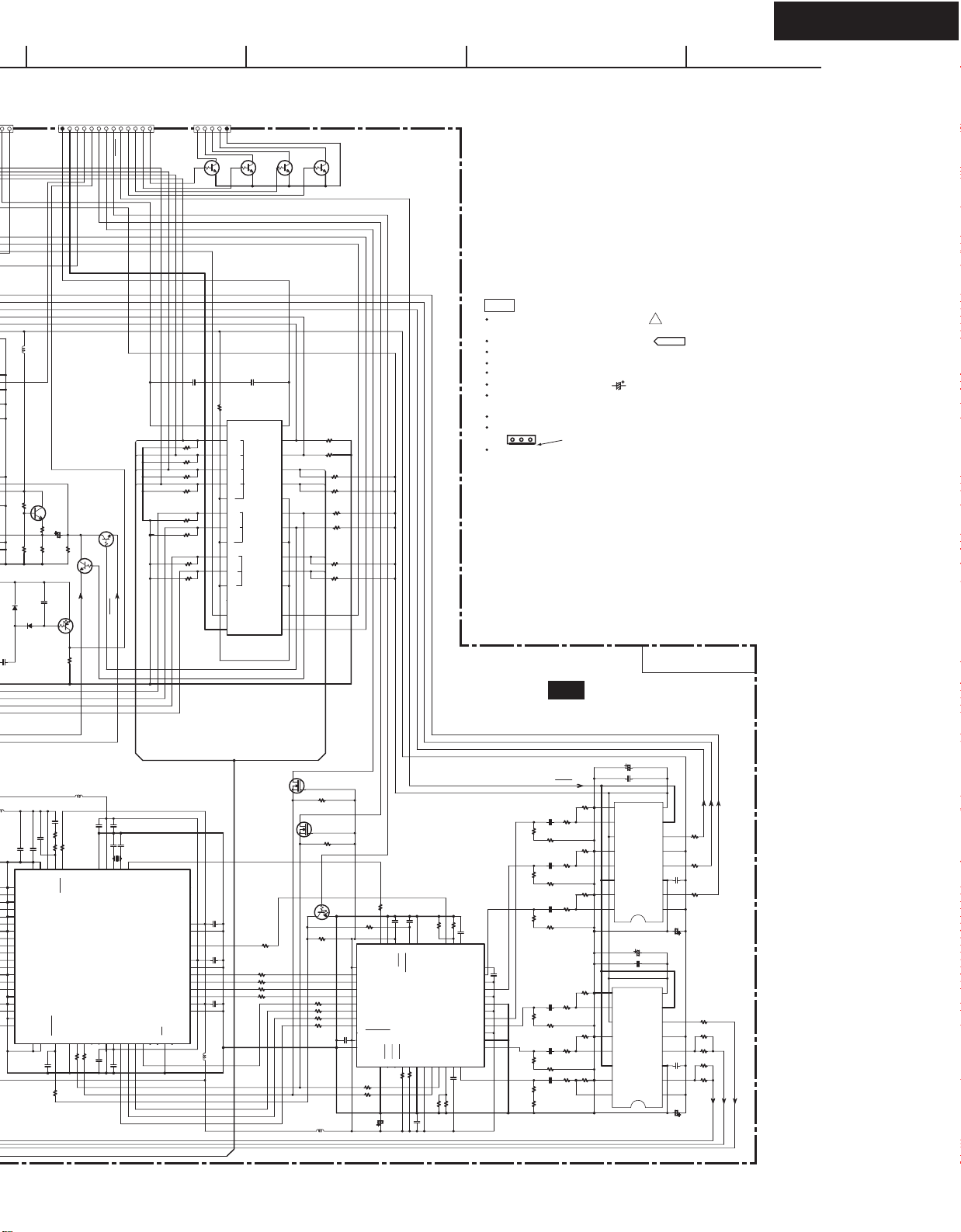
-12V
TO NAETC-8537TO NADG-8514
Q2051
RN1401
JL2006
RN1401
Q2052
Q2053
RN1401
Q2054
RN1401
P2005
V4
+12V
GND
VSYNC
SYNCDET
ISS
SCL
SDA
VMUT
VDRST
NOTE
THE COMPONENTS IDENTIFIED BY MARK ARE CRITICAL FOR SAFETY
REPLACE ONLY WITH PART NUMBER SPECIFIED.
022K
L2002
C2060
270J
C2059
220J
2SC2712-GR
Q2005
6.8K
C2053
100/16
R2048
1K
R2046
47K
3.3K
R2049
R2047
68
C2068
D2002
1SS352
D2003
1SS352
Q2010
RN2402
Q2007
RN1443
104Z
R2045
R2065
Q2006
RN1443
10K
R-S6
R-S5
SDET
SDET
10K
L-S4
L-S5
L-S6
L-S3
L-S2
R2071
R2072
R2073
R2074
R2075
R2076
L-S7
C2072
L-S1
100K
100K
100K
100K
100K
100K
R2077
100K
R2078
100K
L-S8
104Z
C2071
104Z
22
R2070
1
2
3
4
5
6
7
8
9
Q2111 NJM7313A
10
11
12
13
14
DATA
STB
CLK
GND
15 16
R-S1
R-S2
30
29
28
27
26
25
24
23
22
21
20
19
18
17
R-S5
R-S6
R-S3
R-S4
R-S7
R-S8
R2083
100K
R2082
100K
R2086
100K
R2085
100K
R2081
100K
R2080
100K
R2079
100K
R2084
100K
VOLTAGE (MEASURED WITH VOLTMETER) IS DC VOLTAGE.(NO INPUT SIGNAL).
ALL PNP TRANSISTORS ARE EQUIVALENT TO 2SA1015-GR UNLESS OTHERWISE NOTED.
ALL NPN TRANSISTORS ARE EQUIVALENT TO 2SC1815-GR UNLESS OTHERWISE NOTED.
ALL DIODES ARE EQUIVALENT TO 1SS133 UNLESS OTHERWISE NOTED.
ELECTROLYTIC CAPACITORS ( ) ARE IN uF/WV.
ALL CAPACITORS ARE IN pF/50WV UNLESS OTHERWISE NOTED.
EX) 030- 3pF 330- 33pF 331- 330pF 333- 0.033uF
ALL RESISTORS ARE IN OHMS 1/4WATTS UNLESS OTHERWISE NOTED.
THE THICK LINES ON PC BOARD ARE THE PRINTING SIDE OF THE PARTS.
EX) PRINTING SIDE
CIRCUIT IS SUBJECT TO CHANGE FOR IMPROVEMENT.
<Note>
NC=No mount of parts.
!
NAVD-8476
U01 VIDEO PC BOARD
C2135103Z
41
42
47
53
56
59
60
AIN843
AIN244
AIN945
AIN346
AGND
CAPY148
CAPY249
AVDD50
REFOUT51
CML52
AGND
CAPC154
CAPC255
AGND
AIN1057
AIN458
104Z
C2134
40
AGND
61
AIN12
C2133
AGND39
AIN662
104Z
C2125
C2132
823J
103J
R2116
1K
R2115
PVDD38
41 : AIN7
42 : AIN1
59 : AIN11
60 : AIN5
NC
63
100
R2109
L2104
NCH-1477
220K
C2130
104Z
680
4.7K
R2114
34
35
36
P033P132
NC
NC
ELPF37
PWRDN
ADV7183A
NC
ALSB66
SCLK68
SDA67
RESET
6569707172
64
100
C2124
R2111100
R2112
DVDD
120J
C2129
31
DGND
Q2101
NC
NC
103Z
C2126
104Z
30
DVDD
DGND
C2131
XTAL29
DVDD
103Z
C2128
X2101
27MHZ
28
XTAL1
P1573
120J
+5VVD
Q2109
2SK3019
R2113
2.2K
SDA
Q2108
2SK3019
R2110
2.2K
25
26
21
P323
P422
P5
P224
NC
P620
LLC2
LLC127
P719
NC
18
NC
17
NC
16
DGND
NC
SFL12
NC
DVDD10
DGND
P8 8
P9 7
P10 6
P11 5
DVDDIO 4
DGND 3
HS 2
VS 1
FIELD
NC
OE79
78
80
C2186
15
104Z
14
13
C2185
11
104Z
9
C2123
104Z
DVDDIO
L2102
220K
NCH-1477
R2121
R2122
R2123
R2124
R2129
33
33
33
33
33
DVDDIO
NC
P1276
P1375
P1474
77
VDRST
R2145
4.7K
R2125
R2126
R2127
R2128
C2188
104Z
L2105
NCH-1477
220K
Q2105
RN1401
33
33
33
33
R2143
100
1
VAA
P02
P13
P24
P35
P46
P57
P68
P79
10
CSO_HSO
VAA
11
GND12
R2133
100
R2132
100
C2164
10/16
R2144
C2189
C2163
33
104Z
CLOCK13
GND
464748
VAA
GND
FIELD
HSYNC
VSYNC/
14
15
R2131
104Z
44
45
VSO
RESET
Q2104
ADV7172
ALSB17
BLANK
16
4.7K
PAL_NTSC 43
GND
18
R2130
4.7K
CLAMP 42
VAA
19
1.2K
R2141
TTX 41
SCLOCK20
1.2K
R2134
C2141
TTXREQ 40
SDATA
21
104Z
SCRESET/RTC39
RSET222
1.2K
R2142
COMP136
RSET1 38
DACA35
DACB
DACC29
DACD28
COMP223
R2135
1.2K
37
VAA
VAA
GND
VAA
VAA
GND
DACE
DACF24
104Z
C2142
104Z
C2161
VREF
C2162
104Z
34
33
32
31
30
27
26
25
R2182
R2181
82
R2187
VMUT
-5VVD
C2176
R2171
105K
82
R2192
R2186
68
C2175
R2169
105K
82
R2191
R2185
68
R2167
C2174
105K
82
R2190
R2184
68
C2173
R2165
105K
82
R2189
R2183
68
C2172
R2163
105K
82
R2188
68
R2161
C2171
105K
68
C2184
100/16
C2183 104Z
Q2107
100K
100K
100K
R2166
100K
R2164
100K
R2162
100K
89
7
6
5
4
3
2
1
LA7106M
-VCC2
NFB3
89
MUTE2
VIN3+
7
10
GND
+VCC
104Z
-VCC2
GND
+VCC
R2178
11
82
12
R2177
13
C2182
82
104Z
14
R2176
15
82
16
C2181
100/16
10
R2175
11
R2180
12
R2174
13
C2178
104Z
R2179
14
15
R2173
100
16
C2177
100/16
-VCC1
6
NFB2
5
VIN2+
4
MUTE1
3
NFB1
2
VIN1+
1
C2180
100/16
C2179
Q2106
LA7106M
NFB3
VIN3+
-VCC1
NFB2
VIN2+
MUTE1
NFB1
VIN1+
VOUT3
DRCTL
VOUT2
VOUT1
MUTE2
VOUT3
DRCTL
VOUT2
VOUT1
Y
CR
CB
18
390
100
390
R2172
100
R2170
100
R2168
100
100
100
100

TX-SR603/603E/8360
A
SCHEMATIC DIAGRAMS-8
VIDEO SECTION
1
IN 3
IN 2
COMPONENT
VIDEO
IN 1
2
OUT
S VIDEO
VIDEO3 IN
3
VIDEO2
VIDEO1
DVD IN
4
MONITOR OUT
5
CYC
C
OUT
CYC
IN
C
OUT
CYC
IN
C
CY
CR
(PR)
CB
(PB)
CR
(PR)
CB
(PB)
CR
(PR)
CB
(PB)
CR
(PR)
CB
(PB)
BCDEFGH
C2128
120J
X2101
27MHZ
LLC127
P1474
26
LLC2
P1375
25
NC
P1276
P323
P224
DVDDIO
DVDDIO 4
NC
NC
77
78
L-S4
L-S3
L-S5
L-S6
P422
DGND
DVDD10
DGND
DGND 3
OE79
TO NAETC-8537TO NADG-8514
L-S2
R2071
L-S7
21
P5
P620
P719
NC
NC
NC
NC
SFL12
NC
P8 8
P9 7
P10 6
P11 5
HS 2
VS 1
FIELD
80
L-S1
100K
R2072
100K
R2073
100K
R2074
100K
R2075
100K
R2076
100K
R2077
100K
R2078
100K
L-S8
18
17
16
15
14
13
11
C2072
104Z
9
C2186
104Z
C2185
104Z
C2123
104Z
DVDDIO
L2102
220K
JL2006
Q2051
RN1401
C2071
22
R2070
1
2
3
4
5
6
7
8
9
10
11
12
13
14
STB
GND
15 16
R2121
R2122
R2123
R2124
NCH-1477
104Z
DATA
RN1401
Q2052
30
29
28
27
26
25
24
23
22
Q2111 NJM7313A
21
20
19
18
17
CLK
R2129
33
33
33
33
33
R-S5
R-S6
Q2053
R-S1
RN1401
R-S2
R-S3
R-S4
R-S7
R-S8
Q2109
2SK3019
R2145
R2125
R2126
R2127
R2128
L2105
NCH-1477
R2083
100K
R2082
100K
R2113
2.2K
Q2108
2SK3019
R2110
2.2K
VDRST
4.7K
C2188
104Z
220K
Q2054
R2086
100K
R2085
100K
R2081
100K
R2080
100K
R2079
100K
R2084
100K
SDA
Q2105
RN1401
33
33
33
33
RN1401
R2143
100
1
VAA
P02
P13
P24
P35
P46
P57
P68
P79
10
CSO_HSO
VAA
11
GND12
R2133
100
R2132
100
C2164
10/16
R2144
NOTE
THE COMPONENTS IDENTIFIED BY MARK ARE CRITICAL FOR SAFETY
REPLACE ONLY WITH PART NUMBER SPECIFIED.
VOLTAGE (MEASURED WITH VOLTMETER) IS DC VOLTAGE.(NO INPUT SIGNAL).
ALL PNP TRANSISTORS ARE EQUIVALENT TO 2SA1015-GR UNLESS OTHERWISE NOTED.
ALL NPN TRANSISTORS ARE EQUIVALENT TO 2SC1815-GR UNLESS OTHERWISE NOTED.
ALL DIODES ARE EQUIVALENT TO 1SS133 UNLESS OTHERWISE NOTED.
ELECTROLYTIC CAPACITORS ( ) ARE IN uF/WV.
ALL CAPACITORS ARE IN pF/50WV UNLESS OTHERWISE NOTED.
EX) 030- 3pF 330- 33pF 331- 330pF 333- 0.033uF
ALL RESISTORS ARE IN OHMS 1/4WATTS UNLESS OTHERWISE NOTED.
THE THICK LINES ON PC BOARD ARE THE PRINTING SIDE OF THE PARTS.
EX) PRINTING SIDE
CIRCUIT IS SUBJECT TO CHANGE FOR IMPROVEMENT.
<Note>
NC=No mount of parts.
!
NAVD-8476
U01 VIDEO PC BOARD
+5VVD
VMUT
-5VVD
C2176
R2171
105K
82
R2192
R2186
68
C2175
R2169
105K
82
R2191
R2185
68
R2167
104Z
R2182
82
R2181
82
R2187
68
R2184
R2183
C2172
C2174
82
C2173
82
105K
C2171
105K
105K
R2190
68
105K
R2189
68
R2188
68
R2165
R2163
R2161
C2189
C2163
33
104Z
CLOCK13
GND
464748
VAA
GND
FIELD
HSYNC
VSYNC/
14
15
R2131
104Z
44
45
VSO
RESET
Q2104
ADV7172
ALSB17
BLANK
16
4.7K
PAL_NTSC 43
GND
18
R2130
4.7K
CLAMP 42
VAA
19
1.2K
R2141
TTX 41
SCLOCK20
1.2K
R2134
C2141
TTXREQ 40
SDATA
21
104Z
SCRESET/RTC39
RSET222
R2135
1.2K
R2142
37
COMP136
RSET1 38
DACA35
VAA
DACB
VAA
GND
VAA
DACC29
DACD28
COMP223
DACF24
1.2K
C2161
VREF
VAA
GND
DACE
104Z
C2142
104Z
C2162
34
33
32
31
30
27
26
25
C2184
100/16
C2183 104Z
Q2107
100K
100K
100K
R2166
100K
R2164
100K
R2162
100K
89
7
6
5
4
3
2
1
LA7106M
-VCC2
NFB3
89
MUTE2
VIN3+
7
10
GND
+VCC
104Z
GND
+VCC
R2178
11
82
12
R2177
13
C2182
82
104Z
14
R2176
15
82
16
C2181
100/16
10
R2175
11
R2180
12
R2174
13
C2178
100
104Z
R2179
14
15
R2173
100
16
C2177
100/16
-VCC1
6
NFB2
5
VIN2+
4
MUTE1
3
NFB1
2
VIN1+
1
C2180
100/16
C2179
Q2106
LA7106M
NFB3
VIN3+
-VCC1
NFB2
VIN2+
MUTE1
NFB1
VIN1+
VOUT3
DRCTL
VOUT2
VOUT1
-VCC2
MUTE2
VOUT3
DRCTL
VOUT2
VOUT1
Y
CR
CB
18
390
390
R2172
100
R2170
100
R2168
100
100
100
100
P2004
10/16
104Z
10/16
Q2004
LC74763-9836
1
Vss
2
XTALIN1
3
XTALOUT1
4
HSYNCOUT
XTALIN2
5
6
XTALOUT2
7
VSYNCOUT
8
OSDCS
9
OSDDATA
10
OSDSCK
SW1
11
SW2
12
SW3
13
SW4
14
15 16
220
220
R2059
R2060
R2061
220
R2067
R2101
1K
R2103
1K
R2105
1K
L2101
NCH-1477
220K
R2107
1K
TO NADG-8514
VCL
VSTB
+5VVD
VDATA
OSDCK
OSDCS
VDGND
OSDDA
022K
L2007
Vdd1
30
R2057
VCOIN
AMPIN
PDOUT
SEPC
SYNCIN
CVCR
CVIN
Vdd2
CVOUTRST
12K
2.7K
FC
Vss
C2065
100/16
103Z
104Z
10/16
C2115
10/16
R2108
29
D2001
28
L2001
056J
27
26
R2054
25
120
24
23
R2052
1.5K
22
21
R2051
20
C2054
0.33/50
19
18
17
2SA1162-GR
C2066
104Z
Q2103
TA48018AF
C2137
R2102
1K
R2104
1K
R2106
1K
C2113
104Z
C2117
10/16
C2120
104Z
1K
47K
R2055
R2053
820K
Q2009
C2112
10/16
C2114
C2119
10/16
R2056
1K
6.8K
C2050
470J
I
104Z
C2105
C2106
C2107
104Z
C2108
C2109
C2056
682J
R2050
R2062
G
2.7K
O
104Z
SYNCDET
VCOOUT
AMPOUT
C2110
C2103
C2104
V4Y
C2058
223J
C2057
1/50
220
33K
C2136
102J
C2116
104Z
C2122
C2118
104Z
-5VVD
474J
C2063
C2061
0.47/50
C2055
122K
C2052
104Z
C2051
470/10
R2063
2.2K
R2064
NCH-1477
104Z
104Z
104Z
C2111
C2121
104Z
104Z
V4C
C2067
104Z
L2103
220K
470/6.3
102J
-12V
68
V4
C2060
270J
C2059
220J
D2002
C2135103Z
41
42
47
53
56
59
60
6.8K
R2048
L2002
R2049
1SS352
D2003
1SS352
AIN843
AIN244
AIN945
AIN346
AGND
CAPY148
CAPY249
AVDD50
REFOUT51
CML52
AGND
CAPC154
CAPC255
AGND
AIN1057
AIN458
P2005
022K
2SC2712-GR
Q2005
C2053
100/16
1K
R2046
47K
3.3K
R2047
104Z
C2068
Q2010
RN2402
C2132
823J
103J
C2133
R2116
104Z
1K
R2115
C2134
40
PVDD38
AGND
AGND39
41 : AIN7
42 : AIN1
59 : AIN11
60 : AIN5
NC
AIN662
AIN12
61
63
104Z
C2125
100
R2109
ISS
GND
+12V
VSYNC
SYNCDET
10K
R2045
Q2007
RN1443
SDET
10K
R2065
L2104
NCH-1477
220K
C2130
104Z
680
4.7K
R2114
34
35
36
P033P132
NC
NC
ELPF37
PWRDN
ADV7183A
NC
ALSB66
SCLK68
SDA67
RESET
6569707172
64
100
R2111100
R2112
SDA
Q2006
RN1443
R-S5
DVDD
C2129
31
DGND
Q2101
NC
NC
103Z
C2124
SCL
R-S6
120J
30
DVDD
DGND
C2126
104Z
VMUT
VDRST
SDET
C2131
103Z
XTAL29
DVDD
28
XTAL1
P1573
NC
P2305A
Y3
Y2
CR3
CB3
P2201
Y
C2202
102K
P2201
Y
P2201
Y
P2202
Y
C2201
102K
VIDEO
P2001
Y
Y
P2002
Y
Y
P2003
Y
Y
P2007
R2019
C2016
R2013
C2003
102K
C2010
R2007
R2004
R2001
C2001
102K
C2021
C2020
C2019
R2019 - 2021
R2021
R2020
C2017
C2018
C2015
C2014
C2013
R2013 - 2015
R201575R2014
C2011
C2012
C2009
C2008
C2007
R2007 - 2009
R2008
R2009
C2002
102K
C2006
C2005
C2004
R2002, 2005, 2006
R200675R2005
R2001-2003
R2003
R2002
R2018 75
R2017
R2016 75
R2012
R2011
R2010
Y1
CR1
CB1
YOUT
L-S1
L-S2
L-S3
L-S4
CBOUT
VDGND
CR2
CB2
104Z
V3C
10/50
V3Y
10/50
V3
75
V2COUT
75
V2YOUT
V2OUT
C2016 - 2018
470J
104Z
V2C
10/50
V2Y
10/50
V2
75
V1COUT
75
V1YOUT
75
V1OUT
C2010 - 2012
470J
104Z
V1C
10/50
V1Y
10/50
V1 SCL
75
104Z
DVDC
10/50
DVDY
10/50
DVD
C-MON
Y-MON
V-MON
10K
330
R2087
R2088
CROUT
4.7M
R2202
R2203
104Z
C2030
104Z
C2026
104Z
C2022
75
+5VVD
R2201
Y
4.7M
CB
CR
RL2201
-
4.7M
RL2202
-
RL2203
-
D2201
2SC2712-GR
Q2201
R2204 1K
14
15
16
V+
100/16
C2031
100/16
100/16
C2023
SW1
Vout2
Q2003 NJM2595M
Vin5
SW5
Vout1
1234567
14
15
16
V+
SW1
Vout2
Q2002 NJM2595M
C2027
Vin5
SW5
Vout1
1234567
14
15
16
V+
SW1
Vout2
Q2001 NJM2595M
Vin5
SW5
Vout1
1234567
R-S6
C2041
100D
C2042
180J
C2043
C2044
C2045
180J
080D
C2046
470J
C2047
470J
C2048
470J
Q2025
RN1443
R-S6
C2101
C2091
C2090
C2092
X2001
14.32MHZ
X2002
17.73MHZ
470J
R2042
2.2K
R2043
2.2K
R2044
2.2K
C2049
1/50
Q2008
2SA1162-GR
R2066
Q2022
2SA1162-GR
Q2102
TA48033AF
I
G
104Z
R2041
2.2K
R2058
220
O
C2102
470/10
+
RL2204
+
-
+
+
13
Vin1
SW3
13
Vin1
SW3
13
Vin1
SW3
R-S1
12
GND
Vin4
12
GND
Vin4
12
GND
Vin4
R2093
R-S5
R2098
Q2202
2SC2712-GR
11
Vout3
SW4
11
Vout3
SW4
11
Vout3
SW4
R2089
8.2
R-S3
R2090
2.2
R-S7
R2092
470
82
Q2018
RN1443
R2097
470
82
R-S4
RL2205
-
D2202
R2205
10
SW2
Vin3
10
SW2
Vin3
10
SW2
Vin3
R-S8
1K
Q2013
RN1443
+
R-S2
Vin2
100/16
V-
C2032
C2033 104Z
89
Vin2
104Z
100/16
V-
C2028
C2029
89
Vin2
100/16
104Z
C2024
C2025
V89
Q2012
RN1443
C2073
470/16
10K
R2091
Q2017
RN1443
Q2020
RN1443
R2096
10K
C2078
470/16
Q2023
RN1443
R2094
120
R2095
120
Q2024
RN1443
R-S5

PC BOARD CONNECTION DIAGRAM
CENTER
AC IN
SPEAKER
FRONT
SPEAKERS
SURROUND BACK
SPEAKERS
SURROUND
SPEAKERS
TX-SR603/603E/8360
ZONE 2
SPEAKERS
VOLTAGE
SELECTOR
F902
P901A
S902
P912
F901
AC OUTLET
P902
F903
U15
NAPS-8533
POWER SUPPLY-1
PC BOARD
SUB
TRANS.
P6602
JL6602B
U20
NAETC-8538
CENTER SPEAKER TERMINAL
PC BOARD
U17
NAPS-8535
POWER SUPPLY-2
PC BOARD
P931B
P931A
P9502A
JL9501B
P6600 P6605 P6607
U19
NAETC-8537
SPEAKER TERMINAL PC BOARD
JL6600BJL6602B JL6603B
JL6952A
P9502
JL5501A
P997
P996
JL2006B
P995
JL6603A
ZONE 2
LINE OUT
P5503
DVD
VIDEO 1 VIDEO 2
P5504
JL5501B
P311B
PRE OUT
SUB WOOFER
F6901
F6902
JL891B
P6000 P6001 P6002 P6003
POWER TRANSFORMER
U18
NAPS-8536
SEC. TERMINAL-1
PC BOARD
JL891A
P891
U05
NASW-8516
HEADPHONE JACK
PC BOARD
PHONES
F9501
JL9501A
P996A
JL6952B
U10
NAPS-8524
SEC. TERMINAL-2
PC BOARD
P997A
P995A
JL831B
U04
NASW-8515
SWITCH PC BOARD
JL6600A
P6000A P6001A
JL831A
U821
P5503A
P6002A P6003A
U22
NAAF-8540
DRIVER AMPLIFIER
PC BOARD
P5504A
Q801
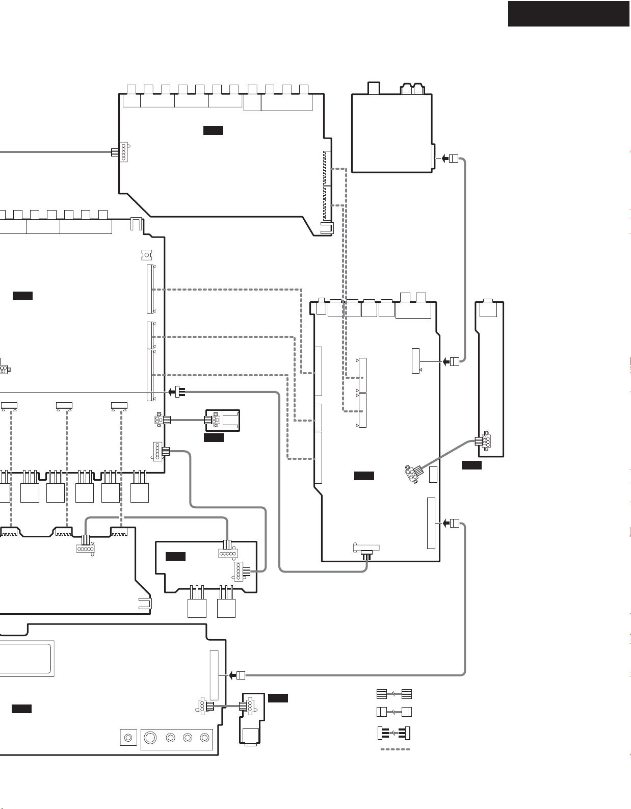
TX-SR603/603E/8360
VIDEO
U09
NAAF-8523
AMPLIFIER PC BOARD
JL5501B
P2004
ANTENNA
FM
TUNER UNIT
DIGITAL
IN 1IN 2IN 3OUT
U131U132
AM
COAXIAL
IN 1
IN 2
P131
P101A
IR IN /
12V TRIGGER OUT
ZONE 2
P121
MONITOR
OUT
P2007
DVD
VIDEO 1 VIDEO 2
P2003
P2002 P2001
COMPONENT VIDEO
VIDEO
3
OUT IN 1 IN 2 IN 3
P2202
P2201
U01
NAVD-8476
JL2006
3
CDTAPE
P7902P7904 P7903P7905P7907 P7906
P303
P301
P302
VIDEO PC BOARD
P2004
P2005
OPTICAL
RI
U133U134
P721
P303A
P6004
P6004A P6005A
U02
NADIS-8513
DISPLAY PC BOARD
JL6006A
P6005
SETUP
JL6402A
JL6200A
Q6055Q6065Q6054Q6064Q6053Q6063Q6052Q6062Q6051Q6061Q6050Q6060
P5019
VIDEO 4 INPUT
S VIDEO VIDEO L-AUDIO-R
MIC
P871
JL6402B
U12
NAETC-8526
THERMAL SENSOR
PC BOARD
JL6006B
U11
NAETC-8525
SBR AMPLIFIER
PC BOARD
JL833A
P872
JL6200B
P701B
Q6056Q6066
Q6380
JL833B
U883
DIGITAL IN
U06
NAETC-8517
FRONT OPT
PC BOARD
P301A
P302A
P2005
JL121B
U03
NADG-8514
DSP PC BOARD
P311A
JL5501B
P751A
P701A
JUMPER WIRE
FLAT CABLE
SOCKET
BOARD TO BOARD
JL121A
U07
NAETC-8518
IR IN TERMINAL
PC BOARD

TX-SR603/603E/8360
6
R21212
R218381
O
O
O
V
V
R218981
R
3
R
6
R
5
R
0
R2079
V
V
-
-1
V
S
A
A
PRINTED CIRCUIT BOARD VIEWS-1
U01
1
2
VIDEO PC BOARD
(NAVD-8476)
ide-
208
208
208
208
BCD
3
4
5

TX-SR603/603E/8360
R216
6
20CC
R218338
1
O
O
O
V
V
R218998
1
R
3
R
R
5
R
0
V
V
-
1
V
A
PRINTED CIRCUIT BOARD VIEWS-2
U01
1
2
VIDEO PC BOARD
(NAVD-8476)
Side-B
BCD
-
208
208
2086
208
3
4
5
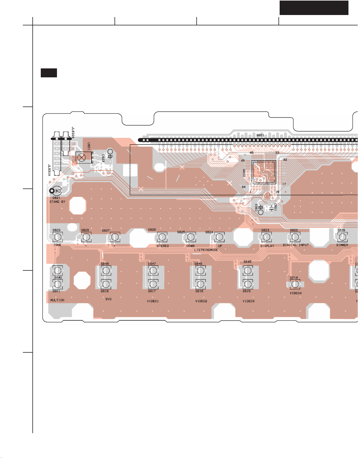
PRINTED CIRCUIT BOARD VIEWS-3
U02
DISPLAY PC BOARD
(NADIS-8513)
Side A
A
1
2
3
4
5
BCDEFGH

TX-SR603/603E/8360TX-SR603/603E/8360
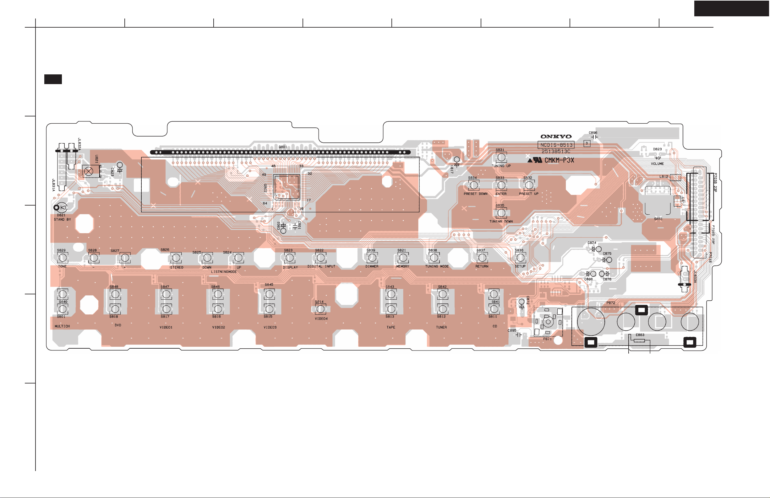
PRINTED CIRCUIT BOARD VIEWS-3
TX-SR603/603E/8360
U02
DISPLAY PC BOARD
(NADIS-8513)
Side A
A
1
2
3
4
5
BCDEFGH
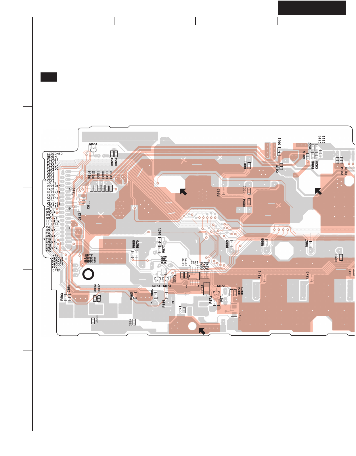
PRINTED CIRCUIT BOARD VIEWS-4
U02
DISPLAY PC BOARD
(NADIS-8513)
Side B
A
1
2
3
4
5
BCDEFGH

TX-SR603/603E/8360TX-SR603/603E/8360

PRINTED CIRCUIT BOARD VIEWS-4
TX-SR603/603E/8360
U02
DISPLAY PC BOARD
(NADIS-8513)
Side B
A
1
2
3
4
5
BCDEFGH

PRINTED CIRCUIT BOARD VIEWS-5
U03
DSP PC BOARD
(NADG-8514)
Side A
A
1
2
3
4
5
BCDEFGH
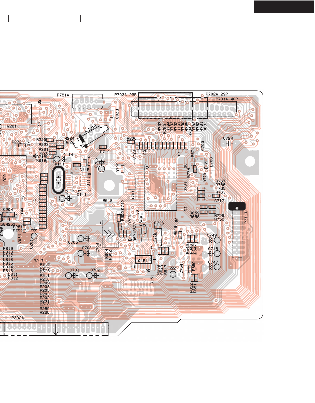
TX-SR603/603E/8360TX-SR603/603E/8360

PRINTED CIRCUIT BOARD VIEWS-5
TX-SR603/603E/8360
U03
DSP PC BOARD
(NADG-8514)
Side A
A
1
2
3
4
5
BCDEFGH

PRINTED CIRCUIT BOARD VIEWS-6
U03
DSP PC BOARD
(NADG-8514)
Side B
A
1
2
3
4
5
BCDEFGH
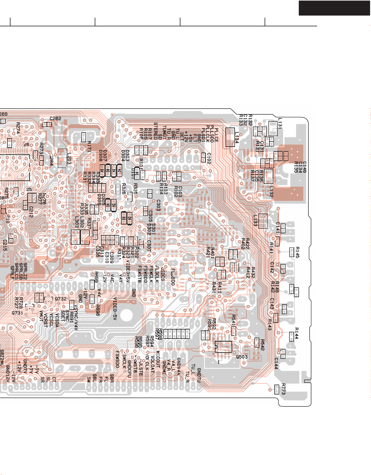
TX-SR603/603E/8360TX-SR603/603E/8360

PRINTED CIRCUIT BOARD VIEWS-6
TX-SR603/603E/8360
U03
DSP PC BOARD
(NADG-8514)
Side B
A
1
2
3
4
5
BCDEFGH

TX-SR603/603E/8360
(
)
S
A
A
PRINTED CIRCUIT BOARD VIEWS-7
U04
1
2
SWITCH PC BOARD
(NASW-8515)
Side A Side B
BCD
3
U05
4
HEADPHONE JACK PC BOARD
NAETC-8516
ide
Side B
5

TX-SR603/603E/8360
A
PRINTED CIRCUIT BOARD VIEWS-8
U06
1
2
FRONT OPT PC BOARD
(NAETC-8517)
Side-A Side-B
BCD
U07
3
IR IN TERMINAL PC BOARD
(NAETC-8518)
Side-A
4
Side-B
5

PRINTED CIRCUIT BOARD VIEWS-9
C
C560
C5603
C560
C5560
C5562
C5556
C5558
C5561
C5563
C5559
C5557
C5576
C5577
C5573
C5572
C5574
C5578
C5550
C5553
C5552
C5551
C5554
C5555
C5666
C5667
C5674
C5673
J5582
J5583
C5566
C5567
C5609
J5570
C5564
C5565
J5598
J5615
J5599
J5614
J5617
J5603
J5602
J5601
J5600
J5619
J5581
C5664
C5665
J5635
J5613
J5611
J5597
J5595
J5566
J5565
J5564
J5563
J5562
J5561
J5560
J5559
J5544
J5545
J5543
J5542
J5541
J5540
J5539
J5513
J5518
J5517
J5512
J5516
J5596
J5612
J5594
J5593
R5707
R5703
R5701
R5705
J5524
J5520
C5575
J5521
J5522
J5523
J5567
J5568
J5569
C5669
C5668
J5616
J5546
J5528
J5548
J5547
C5671
C5672
J5549
J5526
J5511 J5536
J5558 J5580
J5609 J5631
J5534 J5557 J5592 J56
J56
J56
J5590
J5591
J5555
J5556
J5632
J5633
J5587
J5588
J5537
J5538
J5578
J5610
J5634
J5589
J5554 J5579 J5630
J5629J5607
J5608
J5577
P5505
J5552
JL6200A
J5509
J5510
J5508
J5505
J5507
J5506
J5531 J5533
J5576
J5627
J5585
J5606 J562
J5584
P303
P302
J5535
J5532
J5553
J5586
J5628
C5504C5503
J5502
R5682
R5664
J5574
J5573
J5572
J5571
J5527
J5525
R5666
R5667
Q5655
C5641
C5642
C5643
J5550
J5551
C5653
C5652
J5504
J5529
J5530
J5519
J5514
C5660
C5661
C5640
C5650
C5651
R5672
R5671
D5650
J5501
R5665
D5671
D5672
Q5653
Q5650
R5650
R5640
J5575
R5651
J5604
R5660
R5661
JL5501B
J5623
J5605
J5622
J5625
R5668
JL6402A
J5503
J5618
J5515
2
NCAF-8523
25138523B
E301A
P7901
P7902
P7903
P7904
P6846
J5621
J5644
C5663
C5662
J5624
P301
5VDSP
GND
POFF
10S
+5V_V
-5V_V
GND_V
GND_V
12V_TRI
5V_DIS
3.3V_DSP
2.5V_DSP
GND_DSP
GND_DSP
ADLT+
ADLT-
ADRT+
ADRT-
Z2MUT
AMUT
SBMUT
GND_12V
-12V
+12V
GND_7V
+7V
-7V
DAC_SR
DAC_SL
DAC_CT
DAC_SW
DAC_SBL
DAC_FR
DAC_FL
DAC_SBR
FSWDAT
FSWCLK
DGND
FSWSTB
VLTNSTB
VLTNCLK
VLTNDAT
MIC
GND_MIC
V4R
V4L
GND_V4
TUPACK_R
TUPACK_L
GND_TU
C6042
R6082
R601
R600
R60
BE
D6013
ID-ID+
NF
-B1
B+
B-
EB
E
B
BE
BE
R6183
D6003
R6173
R6163
R6143
P6083
J6051
R6193
C6053
Q6073
R6153
J5813
Q6043
C6043
R6083
R6073
Q6033
Q6023
R6023
R6013
R6003
R6033
R6043
R6053
+B1
P6003
Q6063
R6093
R6103
Q6013
J5803
Q6053
BE
D6014
ID-ID+
NF
-B1
B+
B-
EB
E
B
BE
BE
R6184
D6004
R6174
R6164
R6144
P6084
J6052
R6194
C6054
Q6074
R6154
J5812
Q6044
C6044
R6084
R6074
Q6034
Q6024
R6024
R6014
R6004
R6034
R6044
R6054
+B1
P6004
Q6064
R6094
R6104
Q6014
J5802
Q6054
BE
D6015
ID-ID+
NF
-B1
B+
B-
EB
E
B
BE
BE
R6185
D6005
R6175
R6165
R6145
P6085
J6053
R6195
C6055
Q6075
R6155
J5811
Q6045
C6045
R6085
R6075
Q6035
Q6025
R6025
R6015
R6005
R6035
R6045
R6055
+B1
P6005
Q6065
R6095
R6105
Q6015
J5801
Q6055
Q5654
Q5660
Q5640
Q5661
Q5661B
BIAS
BIAS
BIAS
P7901
P7902
P7903
P7904
SL
SR
SBL
J5817
J5818
P6850
P6851
C5565
C5563
C5560
C5558
C5564
C5562
C5559
C5557
C5556
C5566
C5561
C5564C5565
25
20
30
7
7
7
7
17
252525
25
17
20
20
12
15
202020
20
15
12
25
27
30
25
15
15
20
20
12
20
15
15
30
30
25
25
30
7
20
25
22
22
17
20
15 22 15 22 15 22
20
27
27
27
27
20
20
2525 12 12
7
30
27
27
25
25
22
15
25
17
7
30
20
20
22
30
12
27
30
30
30
12
12
20
12
17
20
30
15
30
7
20
25
20
30
12
20
20
U09
AMPLIFIER PC BOARD
(NAAF-8523)
Component side
A
1
2
3
4
5
BCDEFGH

TX-SR603/603E/8360TX-SR603/603E/8360
C5607
C5606
C5600
C5601
C5602
C5603
C5604
C5605
J5640
C5608
P5504
J5691
J5693
J5690
J5705
J5671
J5672
J5692
J5704
J5706
RL5700
RL5700
J5664
J5658
J5659
J5660
J5661
J5662
J5663
D5700
C5664
C5665
C5630
J5653
J5639
J5637
J5636
J5635
J5613
J5638
J5643
J5641
P5503
J011
J010
P995
C6902
C6902
C6901
C6901
C6905
C6904
P997
P996
RL6901
RL6901
RL6902
RL6902
J6105
D6904
D6905
J5710
J5709
J5711
F6901A
F6901B
F6902A
F6902B
C6906
C6907
J6006
J6007
R6902
R6605
C6920
R6901
D6906
Q6901
P9502
JL6952A
JL6951A
J5695
J5712
JL6603A
C6236
R6236
R6235C6235
C6234
R6234
R6233
C6233
C6232
R6232
R6231
C6231
C6230
R6230
J5729
J5730
J5707
J5708
D6901
C6903
D6902
P6906
J5728
J5652
J5668 J5689
J5701
J5651
J5688
J5724
J5722
J5723
J5702
J5703
J5686
J5687
J5649
J5650
-B1
J011A
J010A
J5669
J5670
J5666 J5699
J5735J5725J5700
J5685
J5634 J5667
J5720
J5721
J5732
J5733
J5719
J5717
J5718
J5714
J5715
J5716
J5734
J5682
J5698
J5697
J5684
J5683
J5696
J5646
J5647
J5629
R6701
R6708
B
Q6701
D6702
Q6702
D6701
C6701
R6709
C6706
R6710
D6704
Q6703
R6702
C6703
C6704
R6706
D6703
R6704
J5676
J5679
JL891B
J5731
J5645 J5677J5626
J5648
J5665
J5681
J5680
R6750
R6751
J5737
J5736
R6176
R6186
D6006
J5727
J5726
J5675
J5674
J5738
J5678
J5620
P6844
P6845
J5694
D9005
D9005A
C9010
C9010
JL5501A
C9020
C9020
D9020
C9005
D9011
J5739
J5740
J5742
C9017
P311B
J5673
J5657
C5570
C5571
C5568
C5569
J5654
J5656
J5655
J5743
J5741
C9021
C9021
D5711
C5712
D5710
J5713
J5642
P6011C
P7905
P7906
P7907
P7908
D9021
J5744
+B1
BE
D6010
ID-ID+
NF
-B1
B+
B-
EB
E
B
BE
BE
R6180
D6000
R6170
R6160
R6140
P6080
J6048
R6190
C6050
Q6070
R6150
J5816
Q6040
C6040
R6080
R6070
Q6030
Q6020
R6020
R6010
R6000
R6030
R6040
R6050
+B1
P6000
Q6060
R6090
R6100
Q6010
J5806
Q6050
BE
D6011
ID-ID+
NF
-B1
B+
B-
EB
E
B
BE
BE
R6181
D6001
R6171
R6161
R6141
P6081
J6049
R6191
C6051
Q6071
R6151
J5815
Q6041
C6041
R6081
R6071
Q6031
Q6021
R6021
R6011
R6001
R6031
R6041
R6051
+B1
P6001
Q6061
R6091
R6101
Q6011
J5805
Q6051
BE
D6012
ID-ID+
NF
-B1
B+
B-
EB
E
B
BE
BE
R6182
D6002
R6172
R6162
R6142
P6082
J6050
R6192
C6052
Q6072
R6152
J5814
Q6042
C6042
R6082
R6072
Q6032
Q6022
R6022
R6012
R6002
R6032
R6042
R6052
+B1
P6002
Q6062
R6092
R6102
Q6012
J5804
Q6052
J5746
J5745
FUSE_CHK
8A 125V
F6902
F6901
A
B
BIAS
BIAS
BIAS
P7905
P7906 P7907
P7908
L
R
C
P6849
L
AGND
R
DET
DGND
J
L
6600
A
15
7
7
12
7
12
12
7
7
7
12
15
15
15
20
15
7
30
30
30
15
12
12
20
20
25
25
27
27
27
27
27
27
20
20
1217122525 12
30
30
7
7
30
30
30
7
7
7
15
7
7
7
30
30
12
30
30
7
7
7
30 12
30
20
27
30
30
20
27
12
12
7
12
12
12
7
7
25
25
20

TX-SR603/603E/8360
A
PRINTED CIRCUIT BOARD VIEWS-9
U09
1
2
3
4
5
AMPLIFIER PC BOARD
(NAAF-8523)
Component side
E301A
GND_TU
TUPACK_L
TUPACK_R
GND_V4
V4L
V4R
GND_MIC
MIC
VLTNDAT
VLTNCLK
VLTNSTB
FSWSTB
DGND
FSWCLK
FSWDAT
DAC_SBR
DAC_FL
DAC_FR
DAC_SBL
DAC_SW
DAC_CT
DAC_SL
DAC_SR
-7V
+7V
GND_7V
+12V
-12V
GND_12V
SBMUT
AMUT
Z2MUT
ADRT-
ADRT+
ADLT-
ADLT+
GND_DSP
GND_DSP
2.5V_DSP
3.3V_DSP
5V_DIS
12V_TRI
GND_V
GND_V
-5V_V
+5V_V
POFF
GND
5VDSP
10S
JL6402A
JL6200A
R6035
R6005
R6015
R6085
C6045
J5505
J5506
P303
P301
P302
R6075
J5508
J5510
J5509
P5505
J5514
J5515
J5501
30
30
J5502
7
12
J5519
C5642
C5641
J5504
C5653
Q5655
C5652
30
BIAS
R6045
R6025
J5811
Q6035
BE
Q6025
J5507
15
17
22
J5511 J5536
J5801
Q6055
BCDEFGH
P7901
P7902
P7903
J5516
20
J5503
J5512
20
J5520
P6851
P7901
J5517
15
J5523
J5526
J5525
12
J5530
J5518
15
J5527
D5650
Q5653
J5521
R5666
R5667
C5651
J5524
J5522
J5528
J5818
20
Q5654
J5513
30
20
C5669
J5539
J5550
17
C5650
30
J5529
J5621
C5504C5503
J5540
C5643
Q5650
P7902
J5541
25
25
25
C5668
15
J5542
30
Q5640
J5543
J5546
J5551
20
J5817
12
J5544
30
C5572
C5662
20
J5545
25
J5548
J5547
J5549
J5559
27
C5575
C5671
D5671
J5624
J5560
25
20
J5571
C5640
J5561
12
C5574
C5667
20
C5573
C5672
Q5660
J5644
J5562
15
J5567
17
R5665
J5563
J5568
22
22
J5573
J5564
J5569
C5577
R5671
R5672
J5572
J5575
J5565
202020
C5666
J5574
R5640
R5650
J5566
20
C5576
R5664
12
J5581
J5583
J5582
C5578
J5570
D5672
Q5661
R5701
R5682
P7903
R5703
2
C5565
C5563
C5558
Q5661B
C5663
P6850
C5552
C5551
C5553
R5705
25138523B
NCAF-8523
C5564
C5562
C5560
C5559
C5557
C5566
20
25
30
C5550
C5660
R5707
C5556
J5604
R5660
20
J5605
J5593
15
C5561
R5668
J5594
15
C5564C5565
C5554
C5661
J5595
15
C5674
C5555
C5565
C5558
C5673
J5600
J5596
12
C5563
J5601
J5597
12
J5598
7
C5560
J5602
252525
P7904
J5599
7
C5567
J5603
25
C5557
J5617
17
J5622
J5614
7
C5562
C5559
J5619
17
J5625
J5615
7
C5566
J5623
R5661
R5651
SBL
P6005
+B1
-B1
B+
B-
NF
R6055
ID-ID+
P6085
B
Q6045
J6053
R6195
R6145
C6055
BE
E
J5531 J5533
25
7
J5532
R6105
J5535
15
25
J5534 J5557 J5592 J5651
R6095
Q6015
Q6065
BE
J5552
R6185
R6165
R6155
R6175
Q6075
D6005
25
R6004
R6014
R6084
R6034
C6044
EB
30
27
J5554 J5579 J5630 J5667
D6015
12
22 15 22 15 22 15 22 15 22
J5538
J5537
20
J5556
J5555
BIAS
R6044
R6024
R6074
J5812
BE
Q6034
BE
Q6024
J5576
J5553
R6104
J5558 J5580
27
27
J5802
Q6054
Q6014
P6004
B+
BR6054
+B1
ID-ID+
B
Q6044
J6052
E
30
J5578
BE
-B1
P6084
J5577
SR
J5584
J5585
R6174
Q6074
D6004
22
R6033
R6003
R6013
R6083
C6043
P6846
R6043
R6023
R6073
BE
NF
R6194
20
R6144
C6054
R6184
R6154
R6164
EB
J5586
27
J5589
D6014
J5588
J5587
20 20 20 20
R6094
Q6064
J5609 J5631 J5652
J5591
J5590
Q6053
P6003
J5606 J5645 J5677J5626
BIAS
30 30 12
+B1
-B1
B+
B-
NF
R6053
R6183
ID-ID+
J5813
BE
Q6033
Q6023
Q6043
J6051
E
R6193
R6143
C6053
R6153
P6083
B
J5628 J5648
30
J5803
30
J5608
R6103
27
27
Q6013
J5633
J5632
J5610 J5666 J5699
R6093
Q6063
BE
C5564
J5616
C5556
J5618
SL
R6163
EB
J5611
20
7
C5561
R6173
Q6073
D6013
J5612
20
C5609
JL5501B
25
J5627
D6003
27
P7904
C5665
C5664
20
J5629J5607
J5613
20
C5605
C5603
C5602
R6032
R6002
R6012
R6082
C6042
J5634
J5635
30
7
J5650
J5649
C5606
C5608
J5636
15
C5630
J5641
7
R6042
R6022
R6072
Q6052
C5607
C5601
J5643
C5600
P311B
BE
J5647
J5646
J5637
15
J5640
15
J5642
C5604
R6176
J5620
7
BIAS
Q6032
Q6022
J5804
J5638
15
J5814
20
BE
27
27
J5639
15
R6704
C6703
BR6052
R6102
Q6012
P7905
P7905
C5571
C5569
C5570
C5568
J5654
J5656
P5504
J5655
J5657
P5503
J5661
J5660
P6849
J5659
J5658
RL5700
J5664
RL5700
12
J5663
J5662
D5700
D6703
C6704
R6706
Q6703
D6704
R6708
C6706
R6710
R6709
C6701
R6702
C
P6002
+B1
-B1
B+
NF
R6182
R6162
D6002
R6172
ID-ID+
P6082
B
R6142
Q6042
J6050
E
30
30
J5665
BE
R6192
Q6072
C6052
R6152
EB
20
D6012
J5668 J5689
J5670
J5669
R6092
Q6062
J5673
7
D6701
R6701
J5681
J5680
27
R6081
J5682
J5685
C6901
Q6702
D6006
R6031
R6001
R6011
C6041
7
J5687
J5686
J5688
P7906
P7906 P7907
J5690
J5671
J5672
12
12
12
C6906
C6907
D6905
C6901
J010
J5675
J5674
J5676
Q6701
D6702
B
J5679
7
J5678
R6186
BIAS
R6041
R6021
R6071
J5815
BE
Q6031
BE
Q6021
30
30
J5684
J5683
R6101
27
27
J5805
Q6051
Q6011
30
30
JL6603A
R
P6001
B+
BR6051
+B1
ID-ID+
B
Q6041
E
30
30
BE
J5691
7
J5710
J5709
-B1
P6081
J6049
J5696
J5692
7
NF
R6191
J5701
R6091
J5693
7
P995
R6141
C6051
J5698
J5697
Q6061
J5694
C6905
R6181
R6151
12
J5703
J5702
J5704
7
J5695
12
R6161
EB
7
7
P7907
J5705
7
J5712
12
J5653
R6171
Q6071
D6011
12
J5706
7
D6001
30
P6011C
R6080
J5718
J5717
J5716
J5715
J5714
R6030
R6000
R6010
C6040
7
7
7
D6010
J5723
+B1
J5724
D6904
J6105
J5713
R6230
P7908
P7908
J5708
J5707
J5744
R6020
R6070
Q6050
F6902B
C6902
R6040
BE
J5721
J5720
J5719
F6901B
J5730
J5729
J5711
J010A
C6231
R6232
C6233
R6234
R6236
J5731
7
BIAS
Q6030
Q6020
30
30
J5806
J5816
J5728
J5727
J5726
F6901
F6902
25
25
20
20
15
2520
C6902
C6230
R6231
C6232
R6233
C6234
R6235C6235
C6236
L
P6000
+B1
B+
BR6050
ID-ID+
P6080
B
BE
Q6040
J6048
E
30
30
30
R6100
27
J5722
27
R6090
Q6010
BE
J011
20
-B1
J5734
D5711
C5712
D5710
NF
R6190
J5735J5725J5700
12
12
C6904
R6140
C6050
J5733
J5732
-B1
Q6060
F6902A
JL6951A
B
J5745
JL891B
J5737
J5736
27
R6180
R6160
R6150
7
7
12171225252525 12 12 12
15
J011A
R6751
R6170
EB
F6901A
RL6902
A
J5746
DGND
P6845
D6000
Q6070
RL6901
RL6901
P997
P996
FUSE_CHK
R6750
DET
R
J
L
6600
D6901
C6903
D6902
RL6902
AGND
A
P6844
C9010
L
8A 125V
R6901
JL6952A
C9010
J6007
R6902
J5738
C9021
J5740
12
P6906
25
J5739
J5741
12
D9021
D9005
D9005A
C6920
J6006
R6605
C9021
J5743
D9020
D6906
JL5501A
J5742
7
C9005
Q6901
D9011
P9502
C9017
C9020
C9020
PRINTED CIRCUIT BOARD VIEWS-10
Q5501
Q5501
R5501 R5502
R5700
R5702
R5704
R5706
R5605 R5604
R5602R5603
Q5671
Q5672
Q5630
R5632
R5633
R5634
R5630
R5631
C5631
C5632
R5592
R5593
R5590
R5594
C5590
R5597
R5596
C559
1
R5598
R5595
R5806
R5802
R5663
R5662
R5805
R5807
R5541 R5542
C5501 C5502
R5503
R5543
R5504
R5544
R5506
R5505
R5545
R5546
C5506C5505
R5547
R5507
R5508
R5548
C5508
C5507
C5514
R5554
R5514R5513
R5553
C5513
R5515
R5555
C5515
C5516
R5556
R5516
R5517
R5557
C5517
C5518
R5558
R5518
R5
R5
C5
R5549
C5509
R5550
C5510
R5552
C5512
R5551
C5511
R5681
R5680
R5583
R5582
R5581
R5589
R5588
R5587
D5651
R5804R5803
C5701
C5702
C5703
C5704
C5705
C5706
C5707
R5801
R5810
R5808
R5809
Q5651
Q5652
R5656
R5812
R5811
R5653
R5652
R5655
R5800
R5813
R5814
1
FLAC
FLAC
+24V
-24V
GND
APOWER
POFF
10S
-12V
GND
+12V
-VP
VOLH
THRM
PRO
30
31 50
5180
81
100
1
30
15
16
Q550
2
Q550
2
1
R5599
1
Q550
3
R
5591
U09
AMPLIFIER PC BOARD
(NAAF-8523)
Soldering side
A
1
2
3
4
5
BCDEFGH

TX-SR603/603E/8360TX-SR603/603E/8360
Q5600 Q5610
Q5601 Q5611
R5600
R5610 R5620
R5611 R5621
R5601
R5607
R5627R5617
R5626R5616
R5606
Q5617Q5607
Q5616Q5606
Q5609
Q5608
R5605
R5625R5615
R5624R5614
R5604
Q5615Q5605
Q5614Q5604
Q5602 Q5612
Q5603 Q5613
R5602
R5612 R5622
R5613 R5623
R5603
R5630
C5632
R5619
R
56
18
R5609
R5608
Q5700
P6011A
R5519
R5559
C5519
C5520
R5560
R5520
R5562
C5522
R5522
C5521
R5561
R5521
R5523
C5524
R5564
C5523
R5563
R5524
C5525
R5565
R5525
C5526
R5566
R5526
R5527
C5527
R5567
C5528
R5528
R5568
C5529
R5529
R5569
C5530
R5570
R5530
R5531
C5531
C5532
R5571
R5572
R5532
C5708
C5709
C5710
C5711
P6011B
-VP
FLAC
FLAC
VPOWER
HPDET
APOWER
SEC1H
VOLH
THRM
PRO
1
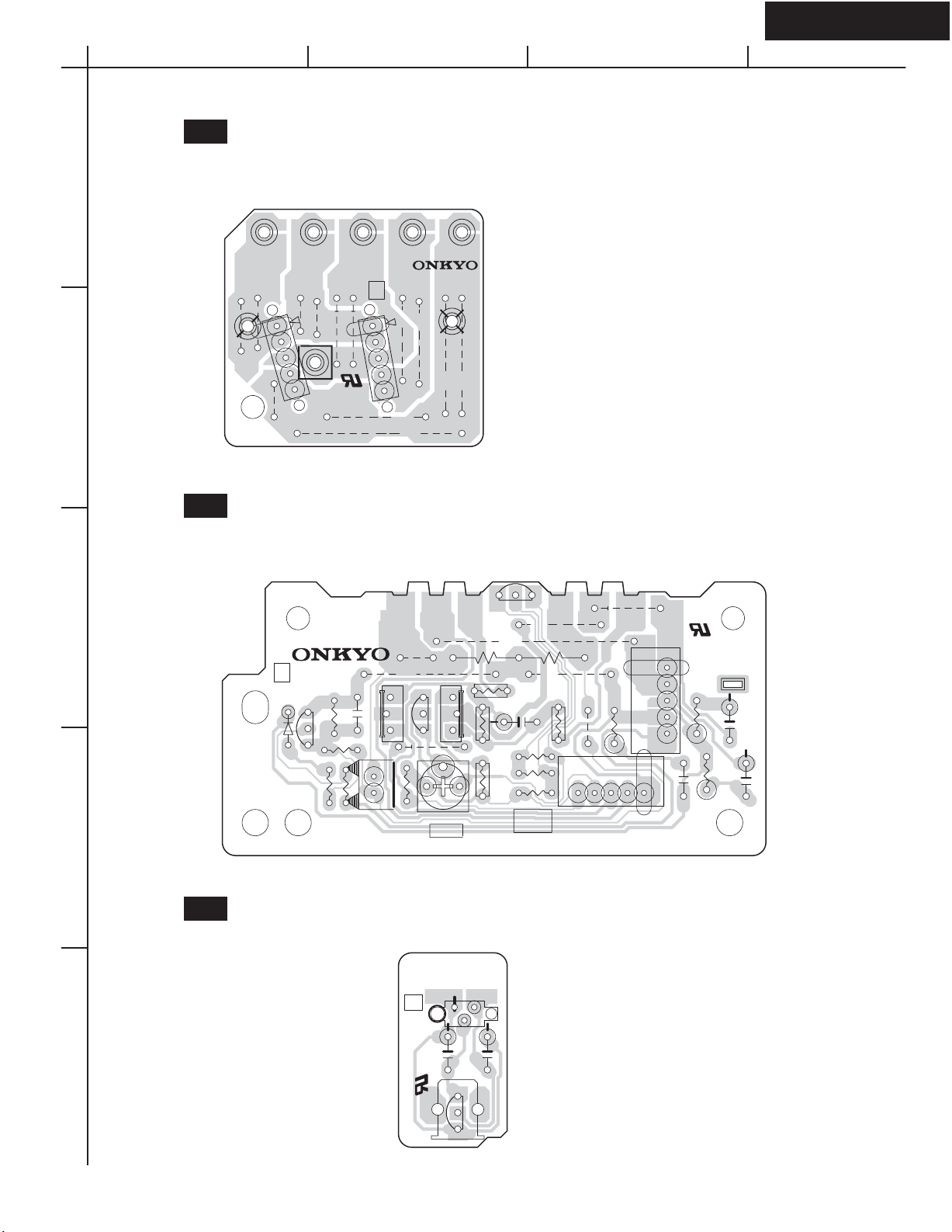
TX-SR603/603E/8360
A
BCD
PRINTED CIRCUIT BOARD VIEWS-11
U10
1
2
SEC. TERMINAL-2 PC BOARD
(NAPS-8524)
Component side
19 18 17 16 15
0
J6406
J6408
P995A
BLK
J6407
J6410
J6404
12
JL6952B
15
25
7
J6412
J6413
P997A
BLU
7
J6409
JL6951B
J6411
NCPS-8524
25138524
12
J6402
J6403
17
J6401
P996A
17
J6405
RED
U11
SBR AMPLIFIER PC BOARD
(NAETC-8525)
Component side
EB
12
J6802
12
R6086
Q6056
J6801
J6803
JL6006B
+B1
J6800
R6136
BBBEE
J6804
JL6200B
SBRSP
C6036
B-
B+
+B1
-B1
IPRO
+B1
-B1
E
NF
P6848
R6515
R6525
C6515
C6525
Q6066
E
Q6076
B
NCETC-8525
25138525
R6156
C6056
R6146
R6166
R6196
ID+
E
Q6046
B
ID-
P6086
R6056
BIAS
J6807
J6805
20
Q6026
E
B
-B1
Q6036
R6046
BIAS
3
1
D6016
4
U12
THERMAL SENSOR PC BOARD
B
E
J6806
R6076
R6026
Q6016
30
R6106
R6096
C6046
SBR
R6016
R6006
R6036
(NAETC-8526)
Component side
JL6402B
0
+5V
THRM
5
MPUGND
C6380
V
NCETC-8526
G
25138526
C6381
O
Q6380
P6380

TX-SR603/603E/8360
A
BCD
PRINTED CIRCUIT BOARD VIEWS-12
U15
1
2
3
4
POWER SUPPLY-1 PC BOARD
(NAPS-8533)
Component side
NNLL
P926
T902
1234
T902
D935
O
G
A
Q930
J921
P931B
POFFVP
+10VS
+12VD
MPUGND
POWERD
D934
J922
R933
7
R932
C932
J919
C931
R934
I
P902
P902
578
56789
D933
C933
R930
C
R931
P925
P917
C930
C922
D930
C922
J911
17
7
J924
D931
D932
D923
F903A
F903
F903B
P918
C921
D922
D924
P909
J905
27
J910
5A 125V
1720
12
J915
RL901
D921
D925
J902
RL901
P912
S902
S902
J903
P912
27
F902A
J906
J909
F902B
12
J908
12
J912
F901A
TRANS-IN
17
J916
17
J918
F901B
7
J923
F901
8A 125V
120V220V
AC-G
AC-GAC-H
AC-H
7
17
J913
C901
J901
J914
C901
0
J900
25138533C
20
T4AL250V
F902
J907
P901A
30 12
AC CORD
J917
NCPS-8533
5

TX-SR603/603E/8360TX-SR603/603E/8360
A
BCDEFGH
PRINTED CIRCUIT BOARD VIEWS-10
U09
1
2
3
AMPLIFIER PC BOARD
(NAAF-8523)
Soldering side
R5804R5803
R5587
R5588
R5589
R5581
R5582
R5583
C5701
R5501 R5502
R5541 R5542
C5501 C5502
16
R5503
R5543
R5805
Q550
R
C5
R5594
R5590
R5520
R5560
C5520
R5608
R5619
R
Q5609
C5708
R5523
R5524
R5525
R5564
R5563
C5523
R5522
R5521
R5562
R5561
C5522
C5521
R5627R5617
Q5617Q5607
Q5616Q5606
R5626R5616
R5625R5615
Q5615Q5605
Q5614Q5604
R5624R5614
R5613 R5623
Q5603 Q5613
Q5602 Q5612
R5612 R5622
R5611 R5621
Q5601 Q5611
Q5600 Q5610
R5610 R5620
Q5608
18
56
C5524
R5565
C5525
R5526
R5566
C5526
C5709
R5527
R5567
C5527
R5528
R5568
C5528
R5529
R5569
C5529
C5710
R5530
R5570
C5530
R5531
R5571
C5531
C5532
R5572
C5711
R5532
P6011B
Q5700
-12V
R5814
10S
R5516
R5556
C5516
R5801
POFF
R5663
R5662
APOWER
GND
-24V
+24V
C5707
R5517
R5557
C5517
FLAC
R5631
Q5630
FLAC
C5631
R5518
R5558
C5518
R5632
R5633
R5634
C5632
R5630
1
R5519
R5559
C5519
R5603
R5602
R5607
R5606
R5605
R5604
R5601
R5600
R5609
5
R5505
R5545
1
9
R5506
R5546
C5506C5505
C5703
R5808
R5507
R5547
C5507
Q5671
Q5672
R5809
R5508
R5548
C5508
100
R5810
R5681
R5802
81
R5807
R5680
R5551
R5552
C5704
C5511
C5512
R5702
R5800
1
R5700
R5704
Q5501
C5705
C5509
R5549
Q5501
R5706
30
5180
R5550
C5510
R5553
C5513
31 50
C5706
R5514R5513
R5554
C5514
R5515
R5555
C5515
R5813
GND
-VP
+12V
C5702
R5504
R5544
1
5
Q550
2
1
Q550
R5592
R5593
R5599
1
3
R5806
C5
R5596
R5598
R5595
R5597
2
30
5591
90
5
D5651
R5812
R5656
4
R5655
Q5652
R5652
R5811
R5653
Q5651
PRO
THRM
VOLH
APOWER
SEC1H
VPOWER
HPDET
FLAC
FLAC
-VP
P6011A
5

TX-SR603/603E/8360
A
BCD
PRINTED CIRCUIT BOARD VIEWS-13
U17
1
2
POWER SUPPLY-2 PC BOARD
(NAPS-8535)
Component side
S3GND
D9706
C9708
D9705
FLAC1
FLAC2
SEC3-2
SEC3-1
SEC2-2
SEC2-1
C9001
D9001
JL9501B
R924
P931A
D9002
J950
D9004
D9003
Q921
B
J964
E
C9003
J960
C9004
R9007
J951
R923
R922
P9002 P9003
J953
J952
J954
C9004
7
7
C9003
J955
J959
J958
J962
J961
J963
D9026
7
J957
FLAC2
FLAC1
R9024
7
+24V
S3GND
P9502A
27
-24V
20
POWER
POFFV
15
D9027
20
+10VS
+12VD
22
25
SEC2-2
MPUGND
C9014
R9004
D9025
NC
-VP
SEC2-1
R9003
D9022
R9002
J956
C9014
D9009
C9009
BE
C9015
D9013
C9009
C9021
R9025
C9016
R9005
C9022
D9023
Q9002
D9012
B
Q9022
R9022
B
B
Q9021
E
D9024
Q9023
E
E
NCPS-8535
25138535
R9023
2
E9001
+10VS
3
U18
SEC. TERMINAL-1 PC BOARD
+12VD
MPUGND
POWERD
POFFVP
(NAPS-8536)
Component side
4
14 13 12 11 10 9 8
NCPS-8536
0
25138536
F9501
2.5A 125V
F9501B
R9591
R9592
C9591
R9594
R9593
F9501A
JL9501A
5
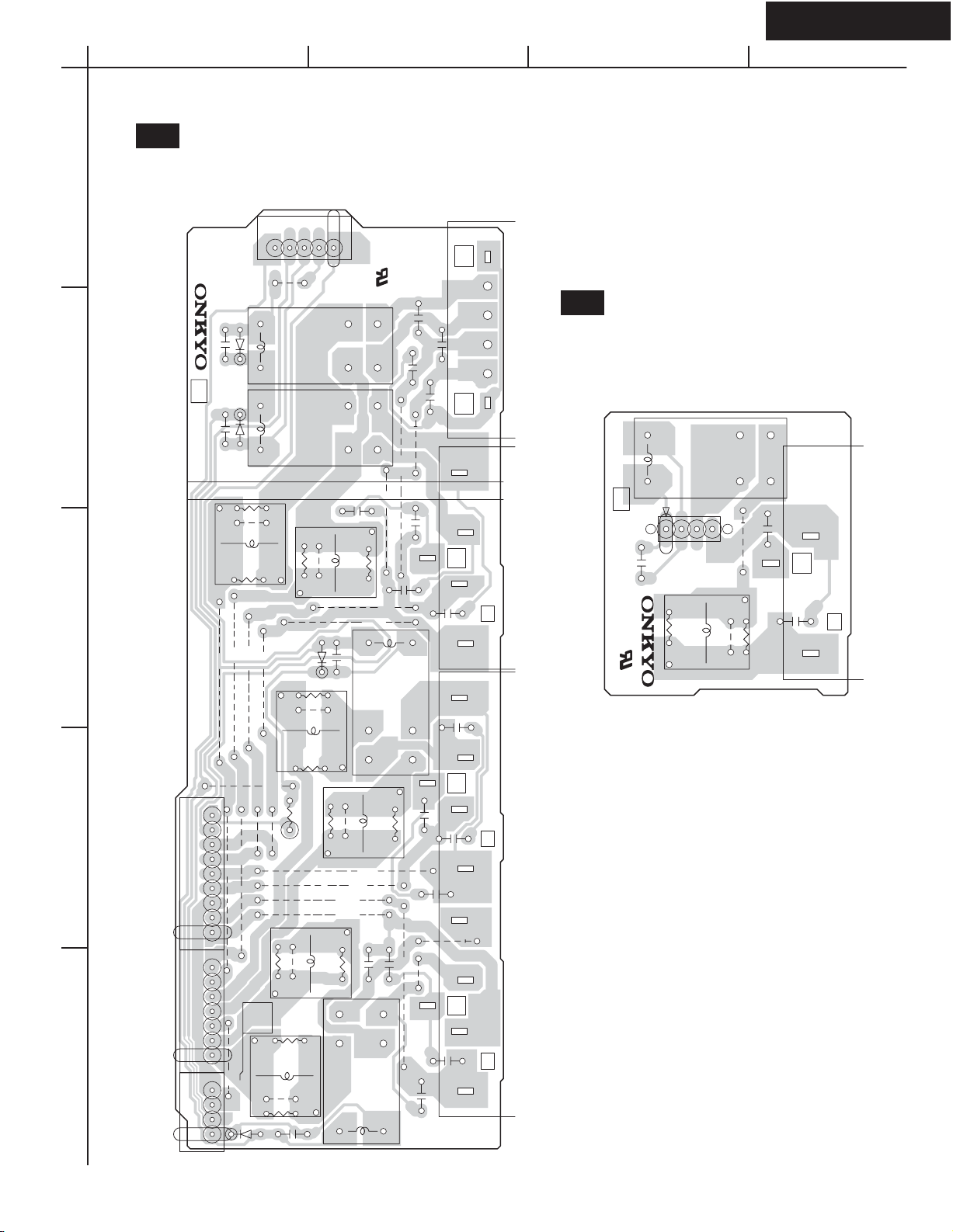
TX-SR603/603E/8360
A
BCD
PRINTED CIRCUIT BOARD VIEWS-14
U19
1
2
3
SPEAKER TERMINAL PC BOARD
(NAETC-8537)
Component side
FRLD
Z2RLD
CSRLD
RLGND
0
25138537
NCETC-8537
L6605
+24V
RLGND
SBRSPE
SBLSPE
SRSPE
SLSPE
CSPE
RSPE
LSPE
SBRLD
C6605 C6607
27
J6618
J6614
D6605 D6607
27
R6605
J6626
L6605
R6615
22
J6617
17
J6616
JL2006B
J6628
J6615
L6604
15
RL6607
RL6607
RL6605
RL6605
L6606
J6621
R6604
J6620
L6604
R6614
R6606
J6622
D6603
J6625
C6656
L6606
C6603
RL6603
R6616
22
17
J6624
C6646
17
RL6603
C6647
C6657
30
J6623
C6648
J6627
C6655
P6605
C6645
C6644
P6607
P6607
C6658
Z2RE Z2LE Z2R Z2L
SBL
SBLE
SBRE SBR
SL
SR
P6605
U20
CENTER SPEAKER TERMINAL
PC BOARD
(NAETC-8538)
Component side
RL6602
RL6602
0
C6652
CSP
L6602
L6602
CSPE
J6851
J6850
R6602
P6602
P6602
C6642
CCE
NCETC-8538
C6602
25138538
JL6602A
CSRLD
+24VR
R6612
30
R6613
L6603
C6650
C6653
27
J6609
J6602
C6651
RL6600
R6690
7
7
4
5
JL6603B
25
27
J6603
SBRSP
SBLSP
SRSP
SLSP
CSP
RSP
LSP
CSPE
CSP
JL6600B
CSPD
+24VR
J6601
12
JL6602B
D6600
J6613
J6605
J6612
R6601
L6601
L6600
R6610
L6600
J6600
R6600
C6600
J6611
J6608
J6607
J6606
J6604
R6611
L6601
R6603
J6619
22
22
L6603
25
C6640
RL6600
C6643
C6654
P6600
C6641
L
J6610
LE
SLE
SRE
P6600
R
RE

TX-SR603/603E/8360
A
BCD
PRINTED CIRCUIT BOARD VIEWS-15
U22
1
2
3
4
5
DRIVER AMPLIFIER
PC BOARD
(NAAF-8540)
Component side
SBR
SBL
P5504A
E
E
SR
E
SL
E
C
E
R
E
L
P5019
E
B
C5045
SBL
E
B
C5046
E
B
C5044
E
B
C5043
25138540
NCAF-8540
0
J5008
20
J5012
P5503A
R5000
C5010
C5000 C5030
Q5005
R5025
R5005
Q5006
R5026
R5006
Q5004
R5024
R5004
Q5003
R5023
R5003
R5040
Q5015
D5005
E
E
R5055
J5145
B
B
Q5055
R5115
R5015
R5095
R5045
C5035
C5015
C5005
C5085
P6021
D5006
Q5016
E
E
R5056
J5146
B
B
Q5056
R5116
R5016
R5096
R5046
C5036
C5016
C5006
C5086
SBR
D5004
Q5014
E
E
R5054
J5144
B
B
Q5054
R5114
R5014
R5094
R5044
C5034
C5014
C5004
C5084
SR
D5003
Q5013
E
E
R5053
J5143
B
B
Q5053
R5113
R5013
R5093
R5043
C5033
C5013
C5003
C5083
SL
E
Q5012
Q5002
E
B
B
R5022
C5042
R5012
R5042
C5012
R5002
CR
E
Q5011
Q5001
E
B
B
R5021
C5041
J5010
J5011
R5011
R5041
C5011
R5001
17
R5010
C5040
R5020
B
E
Q5000
B
E
L
R5035
R5036
R5034
R5033
J5142
C5002
J5141
C5001
J5140
Q5010
R5105
C5105
Q5035
R5235
R5106
C5106
Q5036
R5236
R5104
C5104
Q5034
R5234
R5103
C5103
Q5033
R5233
R5052
R5112
C5032
C5082
R5051
R5111
C5031
C5081
R5050
R5110
C5080
R5065
C5115
B
E
R5066
C5116
B
E
R5064
C5114
B
E
R5063
C5113
B
E
E
B
Q5052
E
B
Q5051
E
B
Q5050
R5135
R5136
R5134
R5133
D5002
R5092
R5032
D5001
R5091
R5031
D5000
R5090
R5030
R5175
R5075
R5085C5025
C5095
J5135
R5165
R5195
R5176
R5076
R5086C5026
C5096
J5136
R5166
R5196
R5174
R5074
R5084C5024
C5094
J5134
R5164
R5194
R5173
R5073
R5083C5023
C5093
J5133
R5163
R5193
R5232
R5231
P6011B
R5230
R5102
C5102
Q5032
R5101
C5101
Q5031
R5100
C5100
Q5030
R5205
R5206
R5204
R5203
C5112
B
E
C5111
B
E
C5110
B
E
E
B
E
B
E
B
E
B
R5062
R5132
R5061
R5131
R5060
R5130
Q5045
C5055
R5185
P6022
Q5046
C5056
R5186
Q5044
C5054
R5184
Q5043
C5053
R5183
R5172
C5092
J5132
R5162
R5192
R5171
C5091
J5131
R5161
R5191
R5170
C5090
J5130
R5160
R5190
J5000
30
J5001
17
R5072
R5082C5022
R5071
R5081C5021
R5070
R5080C5020
30
20
R5202
R5201
R5200
J5002
J5003 J5004
JL6006A
E
Q5042
B
C5052
R5182
E
Q5041
B
C5051
R5181
E
Q5040
B
C5050
R5180
NF
-B1
+B1
B+
B-
B+
+B1
NF
12
17
BB+
+B1
-B1
NF
BB+
+B1
-B1
NF
B-
-B1
J5006J5005
BB+
+B1
-B1
NF
J5009
17 17
P6005A
P6003AP6004A
BB+
+B1
-B1
NF
J5007
30
P6001A
J5013
BB+
+B1
-B1
NF
P6000AP6002A

IC BLOCK DIAGRAM AND TERMINAL DESCRIPTIONS-1
Q111: BU1924FS (RDS decoder)-1
BLOCK DIAGRAM
TX-SR603/603E/8360
MUX
Vref
VDD1
VSS1
VDD2
VSS2
100k
(4)
120k
100k
(3)
(5)
Analog
Power supply
(6)
PLL
(12)
Digital
Power supply
(11)
(13) (14) (10)
XI
57kHz
RDS/ARI
XO
anti-aliasing
filter
PLL
1187.5Hz
Reference
clock
8th Switched
capacitor filter
Bi-phase
decoder
VSS3
(7) (8)
Measurement
circuit
(9)
T1 T2
CMP
comparator
Differential
decoder
(16)
(1)
(2)
RCLK
QUAL
RDATA
TERMINAL DESCRIPTION
Pin No.
1
2
3
4
5
6
7
8
9
10
11
12
13
14
15
16
Pin name
QUAL
RDATA
Vref
MUX
VDD1
VSS1
VSS3
CMP
T2
T1
VSS2
VDD2
XI
XO
(N.C.)
RCLK
Description
Output terminal of demodulator quality signal.
Output terminal of demodulator data.
Input terminal of reference voltage.
Input terminal of composite signal.
Analog power supply.
Analog power supply.
Ground.
Input terminal of comparator.
Input terminal for test mode.
Input terminal for test mode.
Digital power supply.
Digital power supply.
Connect to oscillator.
Connect to oscillator.
--Output terminal of demodulator clock.
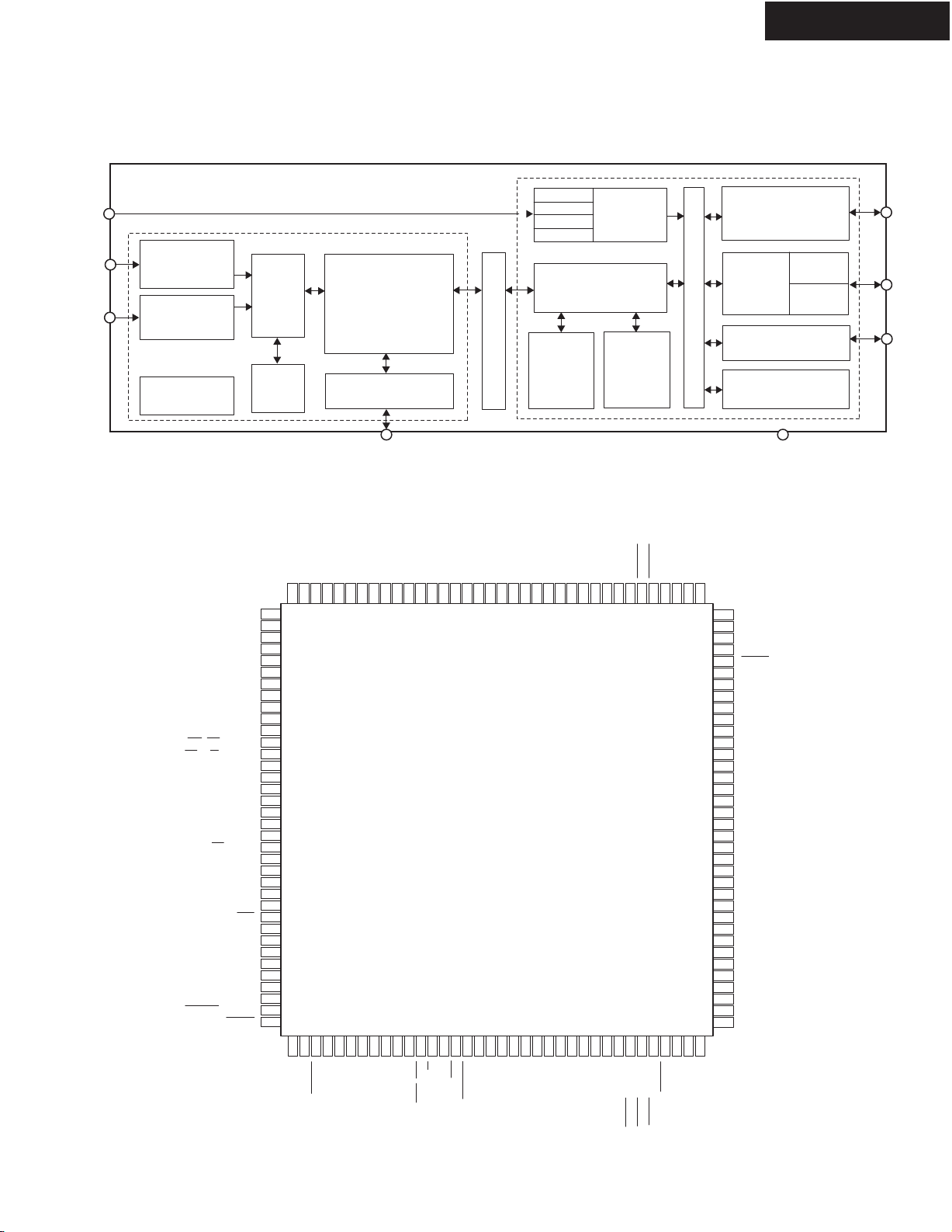
IC BLOCK DIAGRAMS AND TERMINAL DESCRIPTIONS-2
Q201: CS494003CQZ (Multi-Standard Audio Decoder)-1/11
BLOCK DIAGRAM
TX-SR603/603E/8360
Compressed
Digital
Interface
Digital
Audio
Input
DSP AB
PLL Clock
Manager
PIN LAYOUT
CMPCLK, FSCLKN2
HDATA2, GPIO2
HDATA1, GPIO1
HDATA0, GPIO0
CMPREQ, FLRCLKN2
CMPDAT, FSDATAN2
WR, DS, GPIO10
RD, R/W, GPIO11
FSCLKN1, STCCLK2
SCDOUT, SCDIO
HINBSY, GPIO8
UHS2, CS_OUT, GPIO17
AUDATA1
AUDATA0
VSS3
VDD3
FLRCLKN1
PLLVSS
FILT2
FILT1
PLLVDD
XTALO
CLKIN, XTALI
CLKSEL
CS, GPIO9
A0, GPIO13
FSDATAN1
VDD4
VSS4
SCS
SCDIN
VSS5
VDD5
A1, GPIO12
SCCLK
RESET
Frame
Shifter
Input
Buffer
RAM
110
115
120
125
130
135
140
144
LRCLK0
AUDATA2
AUDATA3, XMT958A
HDATA3, GPIO3
105
1
Multi-Standard
Audio decoder
Parallel or Serial
Host Interface
SCLK0
HDATA4, GPIO4
AUDATA4, GPIO28
VSS2
VDD2
MCLK
SCLK1
100
5
10
HDATA5, GPIO5
HDATA6, GPIO6
HDATA7, GPIO7
AUDATA5, GPIO29
AUDATA6, GPIO30
95
15
SAI 0
SAI 1
SAI 2
SAI 3
DSP C
Programmable
32 - Bit DSP
DSP
VDD1
90
NC1
20
NC2
RAM
LRCLK1
SCLKN, GPIO22
LRCLKN, GPIO23
NC3
85
25
NC4
Shared Memory
AUDATA7, XMT958B, GPIO31
VSS1
Serial
Audio
Interface
DSP
ROM
SDATAN0, GPIO24
SDATAN1, GPIO25
SDATAN2, GPIO26
SDATAN3, GPIO27
SD_CAS
SD_RAS
80
30
Internal Bus
SD_ADDR3, EXTA3
SD_ADDR2, EXTA2
SD_ADDR1, EXTA1
SD_ADDR0, EXTA0
75
70
65
60
55
50
45
40
35
External Memory
Interface
Digital
DAO 0
Audio
Output
DAO 1
GPIO and I/O
Controller
Parallel or Serial
Host Interface
SD_ADDR10, EXTA10
SD_BA, EXTA19
VDDSD1
VSSSD1
SD_CS
SD_ADDR4, EXTA4
SD_ADDR5, EXTA5
SD_ADDR6, EXTA6
SD_CLK_EN
SD_ADDR7, EXTA7
SD_ADDR8, EXTA8
SD_CLK_IN
SD_ADDR9, EXTA9
SD_CLK_OUT
VDDSD2
VSSSD2
SD_DATA8, EXTA11
SD_DATA9, EXTA12
SD_DATA10, EXTA13
SD_DATA11, EXTA14
SD_DATA12, EXTA15
VDDSD3
VSSSD3
SD_DATA13, EXTA16
NC5
SD_DATA14, EXTA17
SD_DATA15, EXTA18
SD_DQM1
SD_DATA7, EXTD7
SD_DATA6, EXTD6
VDDSD4
VSSSD4
SD_DATA5, EXTD5
SD_DQM0
SD_DATA4, EXTD4
SD_DATA3, EXTD3
INTREQ
FA1, FSCDIN
UHS0, GPIO18
UHS1, GPIO19
VDD6
FDAT7
GPIO20
GPIO21
FAO, FSCCLK
FHS2, FSCDIO, FSCDOUT
VSS6
FDAT6
FHS0, FWR, FDS
FHS1, FRD, FR/W
FCS
FINTREQ
FDAT5
FDBCK
VDD7
FDAT4
VSS7
FDAT3
FDBDA
DBDA
FDAT2
DBCK
TEST
FDAT1
FDAT0
NV_CS, GPIO14
NV_OE, GPIO15
NV_WE, GPIO16
SD_WE
SD_DATA0, EXTD0
SD_DATA1, EXTD1
SD_DATA2, EXTD2

IC BLOCK DIAGRAMS AND TERMINAL DESCRIPTIONS-3
Q201: CS494003CQZ (Multi-Standard Audio Decoder)-2/11
TERMINAL DESCRIPTION
FILT1 --- Phase-Locked Loop Filter
Connects to an external filter for the on-chip phase-locked loop.
FILT2 --- Phase-Locked Loop Filter
Connects to an external filter for the on-chip phase-locked loop.
CLKIN, XTALI --- External Clock input / Crystal Oscillator input
CS494003 clock input. This pin accepts an external clock input signal that is used to drive the
internal core logic. When in internal clock mode (CLKSEL == VSS), this input is connected to
the internal PLL from which all internal clocks are derived. When in external clock mode
(CLKSEL == VDD), this input is connected to the DSP clock. Alternatively, a 12.288 MHz
crystal oscillator can be connected between XTALI and XTALO. INPUT
TX-SR603/603E/8360
XTALO --- Crystal Oscillator Output
Crystal oscillator output. OUTPUT
CLKSEL --- DSP Clock select
This pin selects the internal source clock. When CLKSEL is low, CLKIN is connected to the
internal PLL from which all internal clocks are derived. When CLKSEL is high, the PLL is
bypassed and the external clock directly drives all input logic. INPUT
FDAT7 --- DSPAB Bidirectional Data Bus
FDAT6
FDAT5
FDAT4
FDAT3
FDAT2
FDAT1
FDAT0
In parallel host mode, these pins provide a bidirectional data bus to DSPAB. These pins have
an internal pull-up.
BIDIRECTIONAL - Default : INPUT
FA0, FSCCLK --- Host Parallel Address Bit Zero or Serial Control Port Clock
In parallel host mode, this pin serves as one of two address input pins used to select one of
four parallel resisters. In serial host mode, this pin serves as the serial control clock signal,
specifically as the SPI clock input. INPUT

TX-SR603/603E/8360
IC BLOCK DIAGRAMS AND TERMINAL DESCRIPTIONS-4
Q201: CS494003CQZ (Multi-Standard Audio Decoder)-3/11
FA1, FSCDIN --- Host Address Bit One or SPI Serial Control Data input
In parallel host mode, this pin serves as one of two address input pins used to select one of
four parallel resisters. In SPI serial host mode, this pin serves as the data input. INPUT
FHS1, FRD, FR/W --- Mode Select Bit 1 or Host Parallel Output Enable or Host Parallel R/W
DSPAB control port mode select bit 1. This bit is one of 3 control port select bits that are
sampled on the rising edge of RESET to determine the control port mode of DSPAB. In Intel
parallel host mode, this pin serves as the active-low data bus enable input. In Motorola parallel
host mode, this pin serves as the read-high/write-low control input signal. In serial host mode,
this pin can serve as the external memory active-low data-enable output signal.
BIDIRECTIONAL - Default: INPUT
FHS0, FWR, FDS --- Mode Select Bit 0 or Host Write Strobe or Host Data Strobe
DSPAB control port mode select bit 0. This bit is one of 3 control port select bits that are
sampled on the rising edge of RESET to determine the control port mode of DSPAB. In Intel
parallel host mode, this pin serves as the active-low data-write-input strobe. In Motorola
parallel host mode, this pin serves as the active-low data-strove-input signal. In serial host
mode, this pin can serves as the external-memory active-low write-enable output signal.
BIDIRECTIONAL - Default: INPUT
FCS --- Host Parallel Chip Select, Host Serial SPI Chip Select
In parallel host mode, this pin serves as the active-low chip-select input signal. In serial host
SPI mode, this pin is used as the active-low chip-select input signal. INPUT
FHS2, FSCDIO, FSCDOUT --- Mode Select Bit 2 or Serial Control Port data Input and Output,
Parallel Port Type Select
DSPAB control port mode select bit 2. This bit is one of 3 control port select bits that are
sampled on the rising edge of RESET to determine the control port mode of DSPAB. In SPI
mode this pin serves as the data output pin. In parallel host mode, this pin is sampled at the
rising edge of RESET to configure the parallel host mode as an Intel type bus or as a
Motorola type bus. BIDIRECTIONAL - Default: INPUT
FINTREQ --- Control Port Interrupt Request
Open-drain interrupt-request output. This pin is driven low to indicate that the DSP has
outgoing control data that should be read by the host.
OPEN DRAIN I/O - Requires 3.3k Ohm Pull - Up
FSCLKN1, STCCLK2 --- PCM Audio Input Bit Clock
Digital-audio bit clock input. FSCLKN1 operates asynchronously from all other DSPAB clocks.
In master mode, FSCLKN1 is derived from DSPAB's internal clock generator. The active edge
of FSCLKN1 can be programmed by the DSP.
BIDIRECTIONAL - Default: INPUT

IC BLOCK DIAGRAMS AND TERMINAL DESCRIPTIONS-5
Q201: CS494003CQZ (Multi-Standard Audio Decoder)-4/11
FLRCLKN1 --- PCM Audio Input Sample Rate clock
Digital-audio frame clock input. FLRCLKN1 typically is run at the sampling frequency.
FLRCLKN1 operates asynchronously from all other DSPAB clocks. The polarity of FLRCLKN1
for a particular subframe can be programmed by the DSP.
BIDIRECTIONAL - Default: INPUT
FSDATAN1 --- PCM Audio Data Input One
Digital-audio data input can accept from one compressed line or 2 channels of PCM data.
FSDATAN1 can be sampled with either edge of FSCLKN1, depending on how FSCLKN1 has
been configured. INPUT
CMPCLK, FSCLKN2 --- PCM Audio Input Bit Clock
Digital- audio bit clock input. FSCKN2 operates asynchronously from all other DSPAB clocks.
The active edge of FSCLKN2 can be programmed by the DSP.
BIDIRECTIONAL - Default: INPUT
TX-SR603/603E/8360
CMPDAT, FSDATAN2 --- PCM Audio Data Input Number Two
Digital-audio data input that can accept either one compressed line or 2 channels of PCM
data. FSDATAN2 can be sampled with either edge of FSCLK2, depending on how FSCLKN2
has been configured.
BIDIRECTIONAL - Default: INPUT
FDBCK --- Reserved
This pin is reserved and should be pulled up with an external 3.3k resistor. INPUT
FDBDA --- Reserved
This pin is reserved and should be pulled up with an external 3.3k resistor.
BIDIRECTIONAL - Default: INPUT
PLLVDD --- PLL Supply Voltage
2.5V PLL supply.
PLLVSS --- PLL Ground Voltage
PLL ground.
RESET --- Master Reset Input
Asynchronous active-low master reset input. Reset should be low at power-up to initialize the
DSP and to guarantee that the device is not active during initial power-on stabilization periods.
At the rising edge of reset the host interface mode of DSPAB is selected contingent on the
state of the FHS0, FHS1, and FHS2 pins. At the rising edge of reset the host interface mode
of DSPC is selected contingent on the state of the UHS0, UHS1, and UHS2 pins. If reset is
low all bidirectional pins are high-Z inputs. INPUT

IC BLOCK DIAGRAMS AND TERMINAL DESCRIPTIONS-6
Q201: CS494003CQZ (Multi-Standard Audio Decoder)-5/11
TEST --- Reserved
This should be tied low for normal operation. INPUT
MCLK --- Audio Master Clock
Bidirectional master audio clock. As an output, MCLK provides a low jitter oversampling clock.
MCLK supports all standard oversampling frequencies. BIDIRECTIONAL - Default: INPUT
SCLK0 --- Audio Output Bit Clock
Bidirectional digital-audio output bit clock for AUDATA0, AUDATA1, AUDATA2, and AUDATA3.
As an output, SCLK0 can provide 32 Fs, 64 Fs, 128 Fs, 256 Fs or 512 Fs frequencies and is
synchronous to MCLK. As an input, SCLK0 is independent of MCLK.
BIDIRECTIONAL - Default: INPUT
TX-SR603/603E/8360
SCLK1 --- Audio Output Bit Clock
Bidirectional digital-audio output bit clock for AUDATA4, AUDATA5, AUDATA6, and AUDATA7.
As an output, SCLK1 can provide 32 Fs, 64 Fs, 128 Fs, 256 Fs, or 512 Fs frequencies and is
synchronous to MCLK. As an input, SCLK1 is independent of MCLK.
BIDIRECTIONAL - Default: INPUT
LRCLK0 --- Audio Output Sample Rate Clock
Bidirectional digital-audio output frame clock for AUDATA0, AUDATA1, AUDATA2, and
AUDATA3. AS an output, LRCLK0 can provide all standard output sample rates up to 192 kHz
and is synchronous to MCLK. As input, LRCLK0 is independent of MCLK.
BIDIRECTIONAL - Default: INPUT
LRCLK1 --- Audio Output Sample Rata Clock
Bidirectional digital-audio output frame clock for AUDATA4, AUDATA5, AUDATA6, and
AUDATA7. AS an output, LRCLK1 can provide all standard output sample rates up to 192 kHz
and is synchronous to MCLK. As input, LRCLK1 is independent of MCLK.
BIDIRECTIONAL - Default: INPUT
AUDATA0 --- Digital Audio Output 0
PCM digital-audio data output. OUTPUT
AUDATA1 --- Digital Audio Output 1
PCM digital-audio data output. OUTPUT
AUDATA2 --- Digital Audio Output 2
PCM digital-audio data output. OUTPUT

IC BLOCK DIAGRAMS AND TERMINAL DESCRIPTIONS-7
Q201: CS494003CQZ (Multi-Standard Audio Decoder)-6/11
AUDATA3, XMT958A --- Digital Audio Output 3, S/PDIF Transmitter
CMOS level output that outputs a biphase-mark encoded (S/PDIF) IEC60958 signal or digital
audio data which is capable of carrying two channels of PCM digital audio. OUTPUT
AUDATA4, GPIO28 --- Digital Audio Output 4, General Purpose I/O
PCM digital-audio data output. This pin can act as a general-purpose input or output that can
be individually configured and controlled by DSPC. BIDIRECTIONAL - Default: OUTPUT
AUDATA5, GPIO29 --- Digital Audio Output 5, General Purpose I/O
PCM digital-audio data output. This pin can act as a general-purpose input or output that can
be individually configured and controlled by DSPC. BIDIRECTIONAL - Default: OUTPUT
AUDATA6, GPIO30 --- Digital Audio Output 6, General Purpose I/O
PCM digital-audio data output. This pin can act as a general-purpose input or output that can
be individually configured and controlled by DSPC. BIDIRECTIONAL - Default: OUTPUT
TX-SR603/603E/8360
AUDATA7, XMT958B, GPIO3 --- Digital Audio Output 7, S/PDIF Transmitter, General Purpose I/O
CMOS level output that contains a biphase-mark encoded (S/PDIF) IEC60958 signal or digital
audio data which is capable of carrying two channels of PCM digital audio. This pin can also
act as a general-purpose input or output that can be individually configured and controlled by
DSCP. BIDIRECTIONAL - Default: OUTPUT
DBCK --- Debug Clock
Must be tied high to 3.3k ohm resistor. INPUT
DBDA --- Debug Data
Must be tied high to 3.3k ohms resistor. BIDIRECTIONAL - Default: INPUT
SLCKN, GPIO22 --- PCM Audio Input Bit Clock, General Purpose I/O
Digital-audio bit clock that is an input. SCLKN operates asynchronously from all other DSPAB
clocks. The active edge of SCLKN can be programmed by the DSP. This pin can act as a
general-purpose input or output that can be individually configured and controlled by DSPC.
BIDIRECTIONAL - Default: INPUT
LRCLKN, GPIO23 --- PCM Audio Input Sample Rate Clock, General Purpose I/O
Digital-audio frame clock input. LRCLKN operates asynchronously from all other DSPAB
clocks. The polarity of LRCLKN for a particular subframe can be programmed by the DSP.
this pin can act as a general-purpose input or output that can be individually configured and
controlled by DSCP. BIDIRECTIONAL - Default: INPUT
SDATAN0, GPIO24 --- PCM Audio Input Data, General Purpose I/O
Digital-audio PCM data input. This pin can act as a general-purpose input or output that can
be individually configured and controlled by DSPC. BIDIRECTIONAL - Default: INPUT

IC BLOCK DIAGRAMS AND TERMINAL DESCRIPTIONS-8
Q201: CS494003CQZ (Multi-Standard Audio Decoder)-7/11
SDATAN1, GPIO25 --- PCM Audio Input Data, General purpose I/O
Digital-audio PCM data input. This can act as a general-purpose input or output that can
be individually configured and controlled by DSPC. BIDIRECTIONAL - Default: INPUT
SDATAN2, GPIO26 --- PCM Audio Input Data, General purpose I/O
Digital-audio PCM data input. This can act as a general-purpose input or output that can
be individually configured and controlled by DSPC. BIDIRECTIONAL - Default: INPUT
SDATAN3, GPIO27 --- PCM Audio Input Data, General purpose I/O
Digital-audio PCM data input. This can act as a general-purpose input or output that can
be individually configured and controlled by DSPC. BIDIRECTIONAL - Default: INPUT
TX-SR603/603E/8360
SCS --- Host Serial SPI Chip Select
SPI mode active-low chip-select input signal. INPUT
SCCLK --- Serial Control Port Clock
This pin serves as the serial SPI clock input. INPUT
SCDIN --- SPI Serial Control Data Input
In SPI mode this pin serves as the data input pin. INPUT
SCDOUT, SCDIO --- Serial Control Port Data Input and Output
In SPI mode this pin serves as the data output pin. BIDIRECTIONAL - Default: OUTPUT in
SPI mode.
INTREQ --- Control Port Interrupt Request
Open-drain interrupt-request output. This pin is driven low to indicate that DSPC has outgoing
control data and should be serviced by the host.
OPEN DRAIN I/O - Requires 3.3k Ohm Pull-Up
HDATA7, GPIO7 --- DSPC Bidirectional Data Bus, General Purpose I/O
HDATA6, GPIO6
HDATA5, GPIO5
HDATA4, GPIO4
HDATA3, GPIO3
HDATA2, GPIO2
HDATA1, GPIO1

IC BLOCK DIAGRAMS AND TERMINAL DESCRIPTIONS-9
Q201: CS494003CQZ (Multi-Standard Audio Decoder)-8/11
HDATA0, GPIO0
In parallel host mode, these pins provide a bidirectional data bus. These pins can also act as
general purpose input or output pins that can be individually configured and controlled by
DSPC. These pins have an internal pull-up. BIDIRECTIONAL - Default: INPUT
A0, GPIO13 --- Host Parallel Address Bit 0, General Purpose I/O
In parallel host mode, this pin serves as the LS Bit of a two bit address input used to select
one of four parallel registers. This pin can act as a general-purpose input or output that can be
individually configured and controlled by DSPC. BIDIRECTIONAL - Default: INPUT
A1, GPIO12 --- Host Address Bit 1, General Purpose I/O
In parallel host mode, this pin serves as the MS Bit of a two bit address input used to select
one of four parallel registers. This pin can act as a general-purpose input or output that can be
individually configured and controlled by DSPC. BIDIRECTIONAL - Default: INPUT
TX-SR603/603E/8360
RD, R/W, GPIO11 --- Host Parallel Output Enable, Host Parallel R/W, General Purpose I/O
In parallel host mode, this pin serves as the active-low data bus enable input. In Motorola
parallel host mode, this pin serves as the read-high/white-low control input signal. This pin can
act as a general-purpose input or output that can be individually configured and controlled by
DSPC. This pin has an internal pull-up. BIDIRECTIONAL - Default: INPUT
WR, DS, GPIO10 --- Host Write Strobe, Host Data Strobe, General Purpose I/O
In Intel parallel host mode, this pin serves as the active-low data bus enable input. In Motorola
parallel host mode, this pin serves as the read-high/write-low control input signal. In serial host
mode, this pin can serve as a general purpose input or output bit. This pin can act as a
general-purpose input or output that can be individually configured and controlled by DSPC.
This pin has an internal pull-up.
BIDIRECTIONAL - Default: INPUT
CS, GPIO9 --- Host Parallel Chip Select, General Purpose I/O
In parallel host mode, this pin serves as the active-low chip-select input signal. This pin can
act as a general-purpose input or output that can be individually configured and controlled by
DSPC. This pin has an internal pull-up. BIDIRECTIONAL - Default: INPUT
HINBSY, GPIO8 --- Input host Message Status, General Purpose I/O
This pin is indicates that serial or parallel communication data written to the DSP has not been
read yet. This pin can act as a general-purpose input or output that can be individually
configured and controlled by DSPC. This pin has an internal pull-up. BIDIRECTIONAL
Default: OUTPUT
SD_DATA15, EXTA18 --- SDRAM Data Bus, SRAM External Address Bus
SD_DATA14, EXTA17
SD_DATA13, EXTA16
SD_DATA12, EXTA15
SD_DATA11, EXTA14
SD_DATA10, EXTA13

IC BLOCK DIAGRAMS AND TERMINAL DESCRIPTIONS-10
Q201: CS494003CQZ (Multi-Standard Audio Decoder)-9/11
SD_DATA9, EXTA12
SD_DATA8, EXTA11
SDRAM data bus 15:8. SRAM external address bus 18:11. OUTPUT
SD_DATA7, EXTD7 --- SDRAM Data Bus, SRAM External Data Bus
SD_DATA6, EXTD6
SD_DATA5, EXTD5
SD_DATA4, EXTD4
SD_DATA3, EXTD3
SD_DATA2, EXTD2
SD_DATA1, EXTD1
SD_DATA0, EXTD0
TX-SR603/603E/8360
SDRAM data bus 7:0. SRAM external data bus 7:0. BIDIRECTIONAL - Default: INPUT
SD_ADDR10, EXTA10 --- SDRAM Address Bus, SRAM External Address Bus
SD_ADDR9, EXTA9
SD_ADDR8, EXTA8
SD_ADDR7, EXTA7
SD_ADDR6, EXTA6
SD_ADDR5, EXTA5
SD_ADDR4, EXTA4
SD_ADDR3, EXTA3
SD_ADDR2, EXTA2
SD_ADDR1, EXTA1
SD_ADDR0, EXTA0
SDRAM address bus 10:0. SRAM external address bus 10:0. OUTPUT
SD_CLK_OUT --- SDRAM Clock Output
SDRAM clock output. OUTPUT
SD_CLK_IN --- SDRAM Re-timing Clock Input
SDRAM re-timing clock input. INPUT
SD_CLK_EN --- SDRAM Clock Enable
SDRAM clock enable. OUTPUT

IC BLOCK DIAGRAMS AND TERMINAL DESCRIPTIONS-11
Q201: CS494003CQZ (Multi-Standard Audio Decoder)-10/11
SD_BA, EXTRA19 --- SDRAM Bank Address Select, SRAM External Address Bus
SDRAM bank address select, SRAM external address bus 19. OUTPUT
SD_CS --- SDRAM Chip select
SDRAM chip select. OUTPUT
SD_RAS --- SDRAM Row Address Strobe
SDRAM row address strobe. OUTPUT
SD_CAS --- SDRAM Column Address Strobe
SDRAM column address strobe. OUTPUT
TX-SR603/603E/8360
SD_WE --- SDRAM Write Enable
SDRAM write enable. OUTPUT
SD_DQM1 --- SDRAM Data Mask 1
SDRAM data mask 1. OUTPUT
SD_DQM0 --- SDRAM Data Mask 2
SDRAM data mask 0. OUTPUT
NV_CS, GPIO14 --- SRAM Chip Select, General Purpose I/O
SRAM/FLASH chip select. This pin can act as a general-purpose input or output that can be
individually configured and controlled by DSPC. BIDIRECTIONAL - Default: OUTPUT
NV_OE, GPIO15 --- SRAM Output Enable, General Purpose I/O
SRAM/FLASH output enable. This pin can act as a general-purpose input or output that can
be individually configured and controlled by DSPC. BIDIRECTIONAL - Default: OUTPUT
NV_WE, GPIO16 --- SRAM Write Enable, General Purpose I/O
SRAM/FLASH write enable. This pin can act as a general-purpose input or output that can be
individually configured and controlled by DSPC. BIDIRECTIONAL - Default: OUTPUT
UHS2, CS_OUT, GPIO17 --- Mode Select Bit 2, External Serial Memory Chip Select,
General Purpose I/O
DSPC control port mode select bit 2. This pin is sampled at the rising edge of RESET and is
one of three pins used to select the control port mode. In serial control port mode, this pin can
serve as an output to provide the chip-select for a serial EEPROM. This pin can act as a
general-purpose input or output that can be individually configured and controlled by DSPC.
BIDIRECTIONAL - Default: INPUT

IC BLOCK DIAGRAMS AND TERMINAL DESCRIPTIONS-12
Q201: CS494003CQZ (Multi-Standard Audio Decoder)-11/11
UHS0, GPIO18 --- Mode Select Bit 0, General Purpose I/O
DSPC control port mode select bit 0. This pin is sampled at the rising edge of RESET and is
one of three pins used to select the control port mode. This pin can act as a general-purpose
input or output that can be individually configured and controlled by DSPC.
BIDIRECTIONAL - Default: INPUT
UHS1, GPIO19 --- Mode Select Bit 1, General Purpose I/O
DSPC control port mode select bit 1. This pin is sampled at the rising edge of RESET and is
one of three pins used to select the control port mode. This pin can act as a general-purpose
input or output that can be individually configured and controlled by DSPC.
BIDIRECTIONAL - Default: INPUT
TX-SR603/603E/8360
GPIO20 --- General Purpose I/O
This pin can act as a general-purpose input or output that can be individually configured and
controlled by DSPC. This pin has an internal pull-up.
BIDIRECTIONAL - Default: INPUT
GPIO21 --- General Purpose I/O
This pin can act as a general-purpose input or output that can be individually configured and
controlled by DSPC. This pin has an internal pull-up.
BIDIRECTIONAL - Default: INPUT
VDD [7:1] --- 2.5V Supply Voltage
2.5V supply voltage.
VSS --- 2.5V Ground
2.5V ground.
NC[5:1] --- No Connect
Recommended tie to ground.
VDDSD [4:1] --- 3.3V SDRAM / SRAM / EPROM Interface Supply
3.3V SDRAM / SRAM / EPROM supply.
VSSSD --- 3.3V SDRAM / SRAM / EPROM interface Ground
3.3V ground.

TX-SR603/603E/8360
IC BLOCK DIAGRAM AND TERMINAL DESCRIPTIONS-13
Q281: MX26LV040 (4M-Bit CMOS Single Voltage 3V Only High Speed Flash Memory)
BLOCK DIAGRAM
#CE
#OE
#WE
A0-A18
CONTROL
INPUT
LOGIC
ADDRESS
LATCH
AND
BUFFER
PROGRAM/ERASE
HIGH VOLTAGE
X-DECODER
MX29LV040
FLASH
ARRAY
Y-DECODER
Y-PASS GATE
SENSE
AMPLIFIER
PROGRAM
DATA LATCH
PGM
DATA
HV
ARRAY
SOURCE
HV
WRITE
STATE
MACHINE
(WSM)
STATE
REGISTER
COMMAND
DATA
DECODER
COMMAND
DATA LATCH
Q0-Q7
I/O BUFFER
PIN LAYOUT TERMINAL DESCRIPTION
A11
A9
A8
A13
A14
A17
WE#
VCC
A18
A16
A15
A12
A7
A6
A5
A4
1
2
3
4
5
6
7
8
9
10
11
12
13
14
15
16
MX26LV040
32
OE#
31
A10
30
CE#
29
Q7
28
Q6
27
Q5
26
Q4
25
Q3
24
GND
23
Q2
22
Q1
21
Q0
20
A0
19
A1
18
A2
17
A3
Pin Name
A0~A18
Q0~Q7
CE#
WE#
OE#
GND
VCC
Description
Address Input
Data Input/Output
Chip Enable Input
Write Enable Input
Output Enable Input
Ground Pin
+3.0V single power supply

IC BLOCK DIAGRAMS AND TERMINAL DESCRIPTIONS-14
Q282: K4S161622H(16Mb H-die SDRAM)-1/2
BLOCK DIAGRAM
TX-SR603/603E/8360
CLK
ADD
Address Register
LCKE
LRAS
Bank Select
Row Buffer
Refresh Counter
LRAS
LCBR
LCBR
LWE
Timing Register
Row Decoder
Col. Buffer
LCAS
Data Input Register
512K x 16
512K x 16
Column Decoder
Latency & Burst Length
Programming Register
LWCBR
Sense AMP
I/O Control
LWE
LDQM
Output Buffer
DQi
LDQM
CLK
CKE
CS
RAS CAS WE L(U)DQM
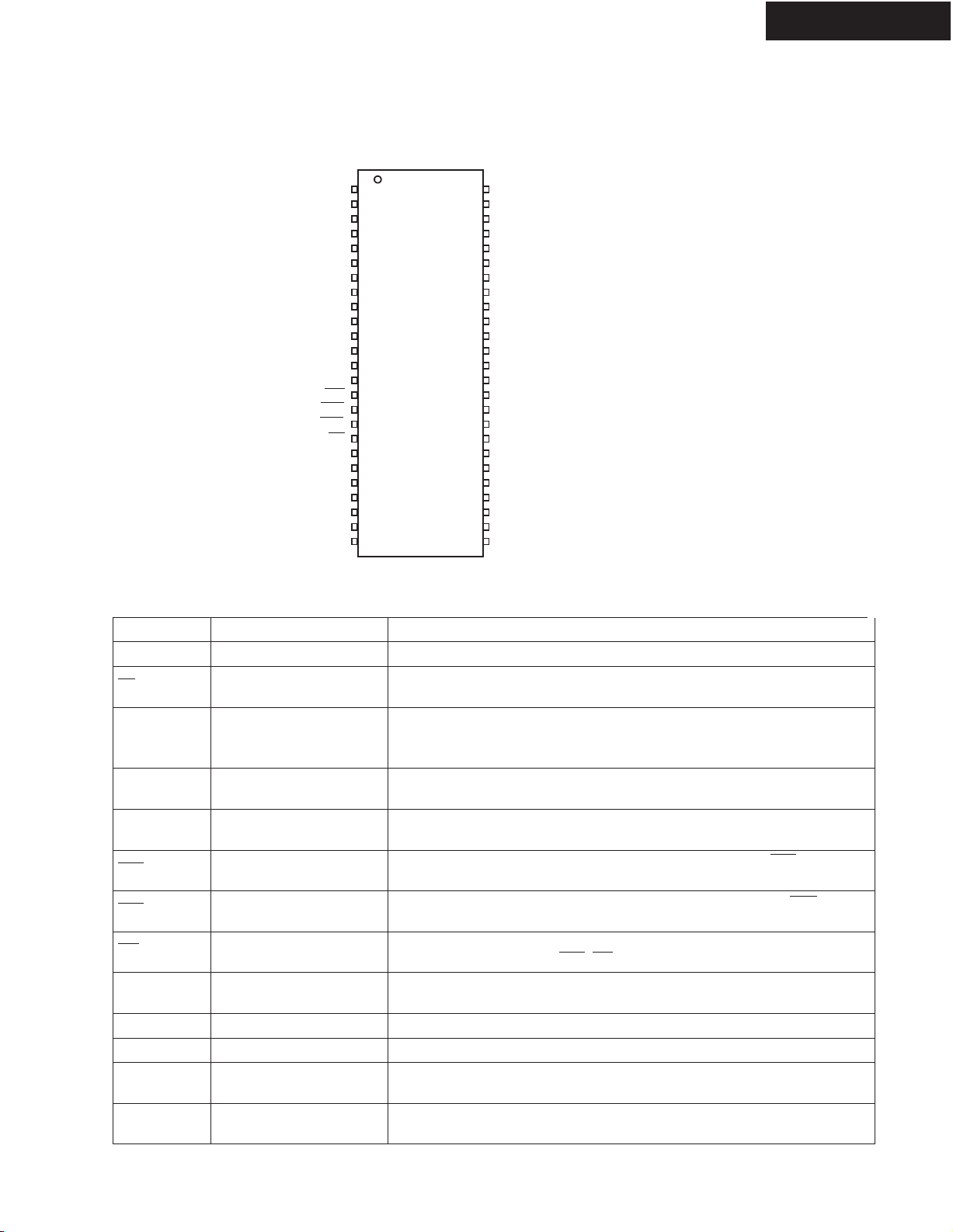
IC BLOCK DIAGRAMS AND TERMINAL DESCRIPTIONS-15
Q282: K4S161622H(16Mb H-die SDRAM)-2/2
PIN LAYOUT
TX-SR603/603E/8360
VSSQ
VDDQ
VSSQ
VDDQ
LDQM
A10/AP
TERMINAL DESCRIPTION
Pin Name
CLK
CS Chip Select
CKE Clock Enable
A0 ~ A10/AP
BA
RAS Row Address Strobe
CAS
WE Write Enable
L(U)DQM
DQ0 ~ 15
VDD/VSS
VDDQ/VSSQ
N.C/RFU
System Clock
Address
Bank Select Address
Column Address Strobe
Data Input/Output Mask
Data Input/Output
Power Supply/Ground
Data Output Power/Ground
No Connection/
Reserved for Future Use
VDD
DQ0
DQ1
DQ2
DQ3
DQ4
DQ5
DQ6
DQ7
WE
CAS
RAS
CS
BA
A0
A1
A2
A3
VDD
1
2
3
4
5
6
7
8
9
10
11
12
13
14
15
16
17
18
19
20
21
22
23
24
25
50
49
48
47
46
45
44
43
42
41
40
39
38
37
36
35
34
33
32
31
30
29
28
27
26
VSS
DQ15
DQ14
VSSQ
DQ13
DQ12
VDDQ
DQ11
DQ10
VSSQ
DQ9
DQ8
VDDQ
N.C/RFU
UDQM
CLK
CKE
N.C
A9
A8
A7
A6
A5
A4
VSS
Function
Active on the positive going edge to sample all inputs.
Disables or enables device operation by masking or enabling all inputs except
CLK, CKE and L(U)DQM
Masks system clock to freeze operation from the next clock cycle.
CKE should be enabled at least one cycle prior to new command.
Disable input buffers for power down in standby.
Row / column addresses are multiplexed on the same pins.
Row address : RA0 ~ RA10, column address : CA0 ~ CA7
Selects bank to be activated during row address latch time.
Selects bank for read/write during column address latch time.
Latches row addresses on the positive going edge of the CLK with RAS low.
Enables row access & precharge.
Latches column addresses on the positive going edge of the CLK with CAS low.
Enables column access.
Enables write operation and row pre-charge.
Latches data in starting from CAS, WE active.
Makes data output Hi-Z, tSHZ after the clock and masks the output.
Blocks data input when L(U)DQM active.
Data inputs/outputs are multiplexed on the same pins.
Power and ground for the input buffers and the core logic.
Isolated power supply and ground for the output buffers to provide improved
noise immunity.
This pin is recommended to be left No Connection on the device.

IC BLOCK DIAGRAMS AND TERMINAL DESCRIPTIONS-16
Q421 : CS42518 (8-Ch Codec with S/PDIF Receiver)-1/4
BLOCK DIAGRAM
TX-SR603/603E/8360
RXP0
RXP1/GPO1
RXP2/GPO2
RXP3/GPO3
RXP4/GPO4
RXP5/GPO5
RXP6/GPO6
RXP7/GPO7
MUTEC
FILT+
VQ
REFGND
VA
AGND
AINL+
AINL-
AINR+
AINR-
AOUTA1+
AOUTA1-
AOUTB1+
AOUTB1-
AOUTA2+
AOUTA2-
AOUTB2+
AOUTB2-
AOUTA3+
AOUTA3-
AOUTB3+
AOUTB3-
AOUTA4+
AOUTA4-
AOUTB4+
AOUTB4-
TXP VARX AGND LPFLT DGND DGND VD
S/P DIF
Decoder
DEM
Gain & Chip
Gain & Chip
Digital Filter
Ref
Rx
GPO
MUTE
ADC#1
ADC#2
Analog Filter
Clock/Data
Recovery
Digital Filter
Digital Filter
DAC#1
DAC#2
DAC#3
DAC#4
DAC#5
DAC#6
DAC#7
DAC#8
C&U Bit
Data Buffer
Format
Detector
Internal MCLK
ADC
Serial
Data
VD
Mult/Div
Interface
Volume Control
Control
Port
Serial
Audio
Port
CODEC
Serial
Port
INT
RST
AD0/CS
AD1/CDIN
SDA/CDOUT
SCL/CCLK
VLC
OMCK
RMCK
SAI_LRCK
SAI_SCLK
SAI_SDOUT
VLS
ADCIN1
ADCIN2
CX_SDOUT
CX_LRCK
CX_SCLK
CX_SDIN1
CX_SDIN2
CX_SDIN3
CX_SDIN4

IC BLOCK DIAGRAMS AND TERMINAL DESCRIPTIONS-17
Q421 : CS42518 (8-Ch Codec with S/PDIF Receiver)-2/4
PIN LAYOUT
CX_SDIN2
CX_SDIN3
CX_SDIN4
SAI_SCLK
SAI_LRCK
OMCK
ADCIN1
ADCIN2
CX_SDOUT
RMCK
SAI_SDOUT
VLS
DGNDVDTXP
RXPO
TX-SR603/603E/8360
CX_SDIN1
CX_SCLK
CX_LRCK
VD
DGND
VLC
SCL/CCLK
SDA/CDOUT
AD1/CDIN
AD0/CS
INT
RST
AINR-
AINR+
AINL+
AINL-
646362616059585756555453525150
1
2
3
4
5
6
7
8
9
10
11
12
13
14
15
16
171819202122232425262728293031
VQ
FILT+
REFGND
CS42518
AOUTB4-
AOUTB4+
VA
AOUTA4-
AOUTA4+
AGND
AOUTB3-
AOUTA3-
AOUTB3+
AOUTA3+
49
32
AOUTB2-
AOUTB2+
AOUTA2+
48
47
46
45
44
43
42
41
40
39
38
37
36
35
34
33
RXP1/GP01
RXP1/GP01
RXP1/GP01
RXP1/GP01
RXP1/GP01
RXP1/GP01
RXP1/GP01
VARX
AGND
LPFLT
MUTEC
AOUTA1AOUTA1+
AOUTB1+
AOUTB1AOUTA2-
TERMINAL DESCRIPTION
Pin Name # Pin Description
CX_SDIN1
CX_SDIN2
CX_SDIN3
CX_SDIN4
CX_SCLK CODEC Serial Clock (Input/Output) - Serial clock for the CODEC serial audio interface
CX_LRCK
VD
DGND
VLC
SCL/CCLK
SDA/CDOUT
AD1/CDIN
1
Codec Serial Audio Data Input (Input) - Input for two's complement serial audio data.
64
63
62
2
3
CODEC Left Right Clock (Input/ Output) - Determines which channel, Left or Right, is currently active on
the CODEC serial audio data line.
4
Digital Power (Input) - Positive power supply for the digital section.
51
5
Digital Ground (Input) - Ground reference. Should be connected to digital ground.
52
6
Control Port Power (Input) - Determines the required signal level for the control port.
7
Serial Control Port Clock (Input) - Serial clock for the serial control port. Requires an external pull-up
resistor to the logic interface voltage in I2C mode as shown in the Typical Connection Diagram.
8
Serial Control Data (Input/Output) - SDA is a data I/O line in IC mode and requires an external pull-up
resistor to the logic interface voltage, as shown in the Typical connection Diagram. CDOUT is the output
data line for the control port interface in SPI mode.
Address Bit 1 (I2C)/Serial Control Data (SPI) (Input) - AD1 a chip address pin in I2C mode; CDIN is
9
the input data line for control port interface in SPI mode.

TX-SR603/603E/8360
IC BLOCK DIAGRAMS AND TERMINAL DESCRIPTIONS-18
Q421 : CS42518 (8-Ch Codec with S/PDIF Receiver)-3/4
Pin Name # Pin Description
AD0/CS 10 Address Bit 0 (I2C)/Control Port Chip Select (SPI) (INput) - AD0 is a chip address pin in I2C mode; CS
is the chip select signal in SPI mode.
INT 11 Interrupt (Ountput) - The CS42518 will generate an interrupt condition as per the Interrupt Mask register.
RST 12 Reset (Input) - The device enters a low power mode and all internal registers are reset to their default
settings when low.
AINRAINR+
AINLAINL+
VQ 17 Quiescent Voltage (Output) - Filter connection for internal quiescent reference voltage.
FILT+ 18 Positive Voltage Reference (Output) - Positive reference voltage for the internal sampling circuits.
REFGND 19 Reference Ground (Input) - Ground reference for the internal sampling circuits.
AOUTA1 +, -
AOUTB1 +, AOUTA2 +, AOUTB2 +, AOUTA3 +, AOUTB3 +, AOUTA4 +, AOUTB4 +, -
VA
VARX
AGND 25
MUTEC 38 Mute Control (Output) - The Mute Control pin outputs high impedance following an initial power -on con-
LPFLT 39 PLL Loop Filer (Output) - An RC network should be connected between this pin and ground.
RXP7/GPO7
RXP6/GPO6
RXP5/GPO5
RXP4/GPO4
RXP3/GPO3
RXP2/GPO2
RXP1/GPO1
RXP0 49 S/PDIF Receiver Input (Input) - Dedicated receiver input for S/PDIF encoded data.
TXP 50 S/PDIF Transmitter Output (Output) - S/PDIF encoded data output, mapped directly from one of the
VLP 53 Serial Port Interface Power (Input) - Determines the required signal level for the serial port interfaces.
SAI_SDOUT 54
RMCK 55 Recovered Master Clock (Output) - Recovered master clock output from the External Clock Reference
13
14
15
16
36, 37
35, 34
32, 33
31, 30
28, 29
27, 26
22, 23
21, 20
24
41
40
42
43
44
45
46
47
48
Differential right Channel Analog Input (Input) - Signals are presented differentially to the delta-sigma
modulators via the AINR+/- pins.
Differential right Channel Analog Input (Input) - Signals are presented differentially to the delta-sigma
modulators via the AINR+/- pins.
Differential Analog Output (Output) - The full-scale differential analog output level is specified in the
Analog Characteristics specification table.
Analog Power (Input) - Positive power supply for the analog section.
Analog Ground (Input) - Ground reference. Should be connected to analog ground.
dition or whenever the PDN bit is set to a "1", forcing the codec into power -down mode. The signal will
remain in a high impedance state as long as the part is in power-down mode. The Mute Control pin goes
to the selected "active" state during reset, muting, or if the master clock to left/right clock frequency ratio
is incorrect. This pin is intended to be used as a control for external mute circuits to prevent the clicks
and pops that can occur in any single supply system. The use of external mute circuits are not mandatoy but may be desired for designs requiring the absolute minimum in extraneous clicks and pops.
S/PDIF Receiver Input/ General Purpose Output (Input/ Output) - Receiver inputs for S/PDIF encoded
data. The CS42518 has an internal 8:2 multiplexer to select the active receiver port, according to the
Receiver Mode Control 2 resister. These pins can also be configured as general purpose output pins,
ADC Overflow indicators or Mute Control outputs according to the RXP/General Purpose Pin Control
resisters.
receiver inputs as indicated by the Receiver Mode Control 2 resister.
Serial Audio Interface Serial Data Output (Output) - Output for two's complement serial audio PCM
data from the S/PDIF incoming stream. This pin can also be configured to transmit the output of the internal and external ADCs.

IC BLOCK DIAGRAMS AND TERMINAL DESCRIPTIONS-19
Q421 : CS42518 (8-Ch Codec with S/PDIF Receiver)-4/4
Pin Name # Pin Description
CL_SDOUT 56 CODEC Serial Data Output (Output) - Output for two's complement serial audio data the internal
and external ADCs.
ADCIN1
ADCIN2
OMCK 59
SAI_LRCK 60
SAI_LRCK 61 Serial Audio Interface Serial Clock (Input/Output) - Serial clock for the Serial Audio Interface
58
57
External ADC Serial Input (Input) - The CS42518 provides for up two external stereo analog to digital
converter inputs to provide a maximum of six channels on serial data output line when the CS42518
is placed in One Line mode.
External Reference Clock (Input) - External clock reference that must be within the ranges specified in
currently active on the serial audio data line.
Serial Audio Interface Left/Right Clock (Input/Output) - Determines which channel, Left of Right, is
currently active on the serial audio data line.
TX-SR603/603E/8360
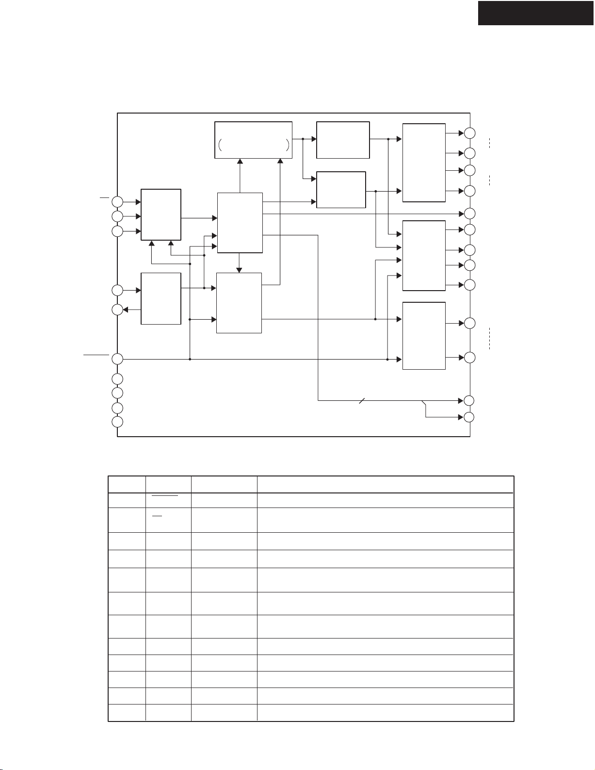
IC BLOCK DIAGRAM AND TERMINAL DESCRIPTIONS-20
Q802: M66005 (FL tube driver)
BLOCK DIAGRAM
TX-SR603/603E/8360
CS
SCK
SDATA
XIN
XOUT
RESET
Vcc1
Vcc2
Vss
Vp
14
15
16
21
20
13
19
60
22
32
Serial
receive
circuit
Clock
generator
data
timing
clock
Display code RAM
Bank 1 : 8bit x 16
Bank 2 : 8bit x 64
code
write
Code/
command
control
circuit
Display
controller
dot data
write
code
select
CGROM
(35bit x 160)
CGRAM
(35bit x 16)
scan pulse
SEG00
59
33
Segment
output
circuit
Segment/
Digit
select/
output
circuit
Digit
output
circuit
2
SEG26
31
SEG27
24
SEG34
SEG35
23
64
DIG12/SEG36
63
DIG13/SEG37
62
DIG14/SEG38
61
DIG15/SEG39
12
DIG00
1
DIG11
P0
18
P1
17
TERMINAL DESCRIPTION
SYMBOL PIN NAME
13
14
15
16
21,
20
1~12
61~64
23~31
33~59
17, 18
19
60
22
32
RESET Reset input This pin is used to initialize the internal state of the M66004.
CS Chip select input
SCK Shift clock input At the rising edge from "L" to "H", input data is shifted.
SDATA Serial data input Character code or command data to display is input from MSB.
XIN,
XOUT
DIG00 ~
Clock input
Clock output
Digit output
DIG15
SEG00 ~
Segment output
SEG39
P0, P1 Output port (static operation)
VCC1
VCC2
VSS GND
VP Negative power supply for VFD drive.
DESCRIPTIONPIN NO.
"L" : Communication with the MCU is possible.
"H" : Any instruction from the MCU is neglected.
This pin is used to connect a resister and a capacitor externally to
set oscillation frequency.
These pins are used to connect to digit pins of VFD.
These pins are used to connect to segment pins of VFD.
Positive power supply for internal logic.
Positive power supply for high-pressure-resistant output port.
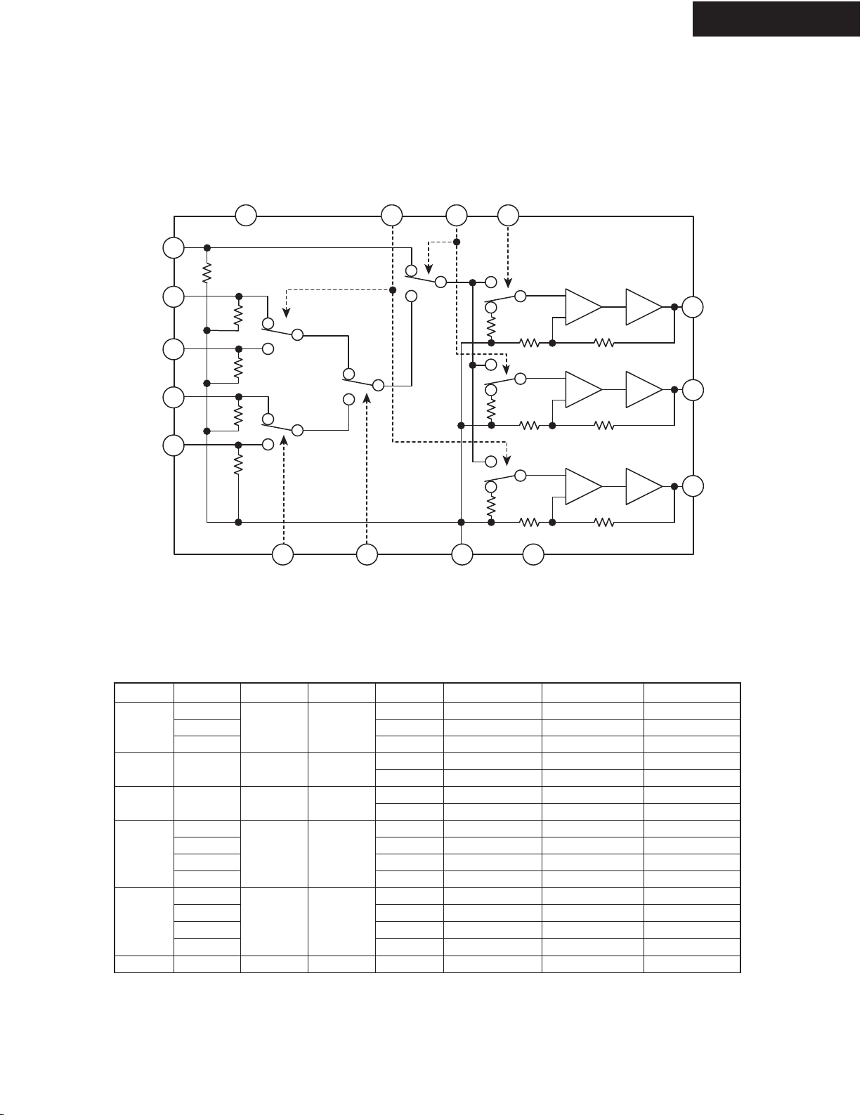
IC BLOCK DIAGRAMS AND TERMINAL DESCRIPTIONS-21
Q2002, 2003: NJM2595(5-INPUT 3-OUTPUT VIDEO SWITCH)
BLOCK DIAGRAM
TX-SR603/603E/8360
Vin1
Vin2
Vin3
Vin4
Vin5
13
9
7
5
3
20k
20k
20k
20k
S2
S3
SW2 SW1V+
1016 214
S4
S1
SW5
20k
20k
20k
S5
S6
S7
6dB
Amp
6dB
Amp
6dB
Amp
75ohms
Driver
75ohms
Driver
75ohms
Driver
1
15
11
Vout1
Vout2
Vout3
81264
V-SW3 SW4 GND
TRUTH TABLE
Control Signal vs. Output Signal (L=VCL, H=VCH, X=L or H)
SW4SW3SW2SW1
H
L
L
X
X
H
H
H
L
H
X
X
L
L
H
H
H
L
L
H
L
H
H
H
L
H
H
L
L
L
X
X
SW5
H
H
L
H
L
H
L
H
L
H
L
H
L
H
L
L
Vout1
Vin1
Vin1
MUTE
Vin2
MUTE
Vin3
MUTE
Vin4
MUTE
Vin4
MUTE
Vin5
MUTE
Vin5
MUTE
MUTE
Vout2
MUTE
MUTE
MUTE
Vin2
Vin2
Vin3
Vin3
Vin4
Vin4
Vin4
Vin4
Vin5
Vin5
Vin5
Vin5
MUTE
Vout3
Vin1
MUTE
Vin1
MUTE
MUTE
Vin3
Vin3
Vin4
Vin4
MUTE
MUTE
Vin5
Vin5
MUTE
MUTE
MUTE

IC BLOCK DIAGRAMS AND TERMINAL DESCRIPTIONS-22
Q2004: LC74763-9836 (On-Screen Display IC) -1/2
BLOCK DIAGRAM
TX-SR603/603E/8360
SIN
SCLK
RST
SECAM
525/625
NTSC/PAL
3.58/4.43
VDD1
VDD2
VSS
SYNCDET
VCOIN
VCOOUT
AMPIN
AMPOUT
PDOUT
CS
FC
Serialparallel
converter
Composite
synchronization
signal
control
AFC
circuit
8-bit latch
and
command
decoder
Sync
detector
Composite
synchronization
signal separator
control
Horizontal
character
size register
Horizontal
size
counter
Vertical
character
size register
Vertical
size
counter
Timing generator
Horizontal
display
position
register
Horizontal
dot counter
Horizontal
display
position
detection
Character
control
counter
Vertical
display
position
register
Vertical
dot counter
Vertical
display
position
detection
Line
control
counter
Synchronization
signal generator
Flashing/
reversal
control
register
Flashing/
reversal
control
circuit
Character output control
Background control
video output control
Display
control
register
RAM write
address
counter
Decoder
Display RAM
Decoder
Font ROM
Shift register
SYSIN
SEPC
Sync
separator
Xtal OUT1
Xtal IN2
Xtal OUT2
VSYNOUTHSYNOUT
Xtal IN1
CVOUTCVINCVCR

IC BLOCK DIAGRAMS AND TERMINAL DESCRIPTIONS-23
Q2004: LC74763-9836 (On-Screen Display IC) -2/2
TERMINAL DESCRIPTION
Pin No. Symbol Function Description
1V
2Xtal
3Xtal
4 HSYNC
5Xtal
6Xtal
7 VSYNC
8 CS Enable input
9 SIN Data input Serial data input (hysteresis input). Pull-up resistor built in (metal option).
10 SCLK Clock input Clock input for serial data input (hysteresis input). Pull-up resistor built in (metal option).
11 SECAM
12 525/625
13 NTSC/PAL
14 3.58/4.43 3.58/4.43 switch input/output During output, functions as general output port or halftone output (command switch).
15 RST Reset input
16 CV
17 V
18 CV
19 CV
20 SYNC
21 SEP
22 V
23 PD
24 AMP
25 AMP
26 FC Control voltage input AFC control voltage input
27 VCO
28 VCO
29 SYNC
30 V
SS
OUT1
OUT2
OUT
DD2
SS
OUT
DD1
Ground Ground connection
IN1
Crystal oscillator connection
Horizontal synchronization Outputs the horizontal synchronization signal (AFC). The output polarity can be selected
OUT
output (metal option). Also functions as general output port (command switch).
IN2
Crystal oscillator connection
Vertical synchronization output
OUT
SECAM mode switch input/
output (command switch)
525/625 switch input/output
(command switch)
NTSC/PAL switch input/output
(command switch)
(command switch) Low = 3.58, high = 4.43
Video signal output Composite video output
Power supply connection Power supply connection for composite video signal level generation
Video signal input Composite video input
IN
Video signal input SECAM chroma signal input
CR
Sync separator circuit input Built-in sync separator circuit video signal input
IN
Sync separator circuit Built-in sync separator circuit
C
Ground Ground connection
Control voltage output AFC control voltage output
IN
AFC filter connection Filter connection
OUT
IN
LC oscillator connection VCO LC oscillator circuit coil and capacitor connection
OUT
External synchronization signal
DET
detection output
Power supply connection
Connection for the crystal and capacitor used to form the crystal oscillator that generates
the internal synchronization signal. The oscillator can be selected with a command switch.
Connection for the crystal and capacitor used to form the crystal oscillator that generates
the internal synchronization signal.
Outputs the vertical synchronization signal. The output polarity can be selected (metal
option). Also functions as general output port (command switch).
Enables/disables serial data input. Serial data is enabled when this pin is low (hysteresis
input). Pull-up resistor built in (metal option).
During input, switches between SECAM and other modes.
During output, functions as general output port or internal V output (command switch).
Low = other modes, high = SECAM mode
During input, switches between 525 scan lines and 625 scan lines.
During output, functions as general output port or character data output (command switch).
Low = 525 lines, high = 625 lines
Switches the color mode between NTSC and PAL.
During output, functions as general output port or frame data output (command switch).
Low = NTSC, high = PAL
Switch FSC between 3.58 MHz and 4.43 MHz.
System reset input pin, low is active (hysteresis input).
Pull-up resistor built in (metal option).
Outputs the exclusive NOR of the horizontal synchronization signal (AFC) and CSYNC (sync
separator). The output polarity can be selected (metal option). Also functions as general
output port (command switch).
Power supply connection (+5 V: digital system power supply)
TX-SR603/603E/8360

TX-SR603/603E/8360
IC BLOCK DIAGRAM AND TERMINAL DESCRIPTIONS-24
Q2101: ADV7183
(Advanced Video Decoder with 10-Bit ADC and Component Input Support)-1/3
BLOCK DIAGRAM
P15-P0
PIXEL
O/P PORT
ISO
REFOUT
AIN1
AIN2
AIN3
AIN4
AIN5
AIN6
ADV7183
ANALOG I/P
MULTIPLEXING
AUTOMATIC
CONTROL
CLAMP AND
DC RESTRE
PWRDN
GAIN
(AGC)
SHAPING
AND
NOTCH LPF
10-BIT
ADC
27MHz
10-BIT
ADC
VIDEO TIMING AND
CONTROL BLOCK
HSYNC FIELD VSYNC HREF VREF CLOCK
LUMA
ANTIALIAS
LPF
SWITCH
PEAKING
HPF/LPF
SUB-
CARRIER
RECOVERY
O
DT
CHROMA
ANTIALIAS
LPF
27MHz XTAL
OSCILLATOR
BLOCK
RESAMPLING
AND
HORIZONTAL
SCALING
SYNC
DETECTION
RESAMPLING
AND
HORIZONTAL
SCALING
SHAPING
LPF
CLOCK
LUMA
DELAY
BLOCK
2H LINE
MEMORY
CHROMA
COMB
FILTER
I2C-COMPATIBLE
INTERFACE PORT
SCLOCKRESET ALSB
SDATA
FIFO CONTROL
BLOCK
AND
PIXEL
OUTPUT
FORMATTER
LLC
SYNTHESIS
WITH LINE-
LOCKED
OUTPUT
CLOCK
AFF
HFF/QCLK
AEF
DV
RD
OE
GL/CLKIN
LLC1
LLC2
LLCREF
ELPF

TX-SR603/603E/8360
IC BLOCK DIAGRAM AND TERMINAL DESCRIPTIONS-25
Q2101: ADV7183
(Advanced Video Decoder with 10-Bit ADC and Component Input Support)-2/3
TERMINAL DESCRIPTION
Pin Mnemonic Input/Output Function
1 VS/VACTIVE O VS or Vertical Sync. A dual-function pin, (OM_SEL[1:0] = 0, 0) is an
output signal that indicates a vertical sync with respect to the YUV pixel
data. The active period of this signal is six lines of video long. The polarity
of the VS signal is controlled by the PVS bit. VACTIVE (OM_SEL[1:0] =
1, 0 or 0, 1) is an output signal that is active during the active/viewable
period of a video field. The polarity of VACTIVE is controlled by PVS bit.
2 HS/HACTIVE O
3, 14 DVSSIO G Digital I/O Ground
4, 15 DVDDIO P Digital I/O Supply Voltage (3.3 V)
5-8, 19-24, P15-P0 O Video Pixel Output Port. 8-bit multiplexed YCrCb pixel port (P15-P8),
32, 33, 73-76
9, 31, 71 DVSS1-3 G Ground for Digital Supply
10, 30, 72 DVDD1-3 P Digital Supply Voltage (3.3 V)
11 AFF O Almost Full Flag. A FIFO control signal indicating when the FIFO has
12 HFF/QCLK/GL I/O Half Full Flag. A multifunction pin, (OM_SEL[1:0] = 1, 0) is a FIFO
13 AEF O Almost Empty Flag. A FIFO control signal, it indicates when the FIFO
16 CLKIN I Asynchronous FIFO Clock. This asynchronous clock is used to output
17, 18, 34, 35 GPO[3:0] O General-Purpose Outputs controlled via I C
25 LLCREF O Clock Reference Output. This is a clock qualifier distributed by the inter-
26 LLC2 O Line-Locked Clock System Output Clock/2 (13.5 MHz)
27 LLC1/PCLK O Line-Locked Clock System Output Clock. A dual-function pin (27 MHz 5%)
28 XTAL1 O Second terminal for crystal oscillator; not connected if external clock
29 XTAL I Input terminal for 27MHz crystal oscillator or connection for external
36 PWRDN I Power-Down Enable. A logical low will place part in a power-down status.
37 ELPF I This pin is used for the External Loop Filter that is required for the LLC PLL.
38 PVDD
39 PVSS
P
G
HS or Horizontal Sync. A dual-function pin, (OM_SEL[1:0] = 0, 0) is a
programmable horizontal sync output signal. The rising and falling edges
can be controlled by HSB[9:0] and HSE[9:0] in steps of 2 LLC1. The polarity
of the HS signal is controlled by the PHS bit. HACTIVE (OM_SEL[1:0]=
1, 0 or 0, 1) is an output signal that is active during the active/viewable
period of a video line. The active portion of a video line is programmable on
the ADV7183. The polarity of HACTIVE is controlled by PHS bit.
16-bit YCrCb pixel port (P15-P8 = Y and P7-P0 = Cb,Cr).
reached the almost full margin set by the user (use FFM[4:0]). The polarity
of this signal is controlled by the PFF bit.
control signal that indicates when the FIFO is half full. The QCLK
(OM_SEL[1:0] = 0, 1) pin function is a qualified pixel output clock when
using FIFO SCAPI mode. The GL (OM_SEL[1:0] = 0, 0) function
(Genlock output) is a signal that contains a serial stream of data that contains
information for locking the subcarrier frequency. The polarity of HFF signal
is controlled by PFF bit.
has reached the almost empty margin set by the user (use FFM[4:0]). The
polarity of this signal is controlled by PFF bit.
data onto the P19-P0 bus and other control signals.
2
nal CGC for a data rate of LLC2. The polarity of LLCREF is controlled
by the PLLCREF bit.
or a FIFO output clock ranging from 20 MHz to 35 MHz.
source is used.
oscillator with CMOS-compatible square wave clock signal
TX-SR603/603E/8360
IC BLOCK DIAGRAM AND TERMINAL DESCRIPTIONS-26
Q2101: ADV7183
(Advanced Video Decoder with 10-Bit ADC and Component Input Support)-3/3
Pin Mnemonic Input/Output Function
40, 47, 53, 56,
63
41, 43, 45, 57,
59, 61
42, 44, 46, 58,
60, 62
48, 49
50
51
52
54, 55
64
65
66
67
68
69
70
77
78
79
80
AVSS
AVSS1-6
AIN1-6
CAPY1-2
AVDD
REFOUT
CML
CAPC1-2
RESET
ISO
ALSB
SDATA
SCLK
VREF/VRESET
HREF/HRESET
RD
DV
OE
FIELD
G
G
I
I
P
O
O
I
I/O
I
I
I/O
I
O
O
I
O
I
O
Ground for Analog Supply
Analog Input Channels. Ground if single-ended mode is selected. These
pins should be connected directly to REFOUT when differential mode is
selected.
Video Analog Input Channels
ADC Capacitor Network
Analog Supply Voltage (5 V)
Internal Voltage Reference Output
Common-Mode Level for ADC
ADC Capacitor Network
System Reset Input. Active Low.
Input Switch Over. A low to high transition on this input indicates to the
decoder core that the input video source has been changed externally and
configures the decoder to reacquire the new timing information of the new
source. This is useful in applications where external video muxes are used.
This input gives the advantage of faster locking to the external muxed
video sources. A low to high transition triggers this input.
TTL Address Input. Selects the MPU address:
MPU address = 88h ALSB = 0, disables I C filter
MPU address = 8Ah ALSB = 1, enables I C filter
MPU Port Serial Data Input/Output
MPU Port Serial Interface Clock Input
VREF or Vertical Reference Output Signal. Indicates start of next field.
VRESET or Vertical Reset Output is a signal that indicates the beginning
of a new field. In SCAPI/CAPI mode this signal is one clock wide and
active low relative to CLKIN. It immediately follows the HRESET pixel,
and indicates that the next active pixel is the first active pixel of the next field.
HREF or Horizontal Reference Output Signal. A dual-function pin
(enabled when Line-Locked Interface is selected, OM_SEL[1:0] = 0,0),
this signal is used to indicate data on the YUV output. The positive slope
indicates the beginning of a new active line; HREF is always 720 Y samples
long. HRESET or Horizontal Reset Output (enabled when SCAPI or
CAPI is selected, OM_SEL[1:0] = 0, 1 or 1, 0) is a signal that indicates the
beginning of a new line of video. In SCAPI/CAPI this signal is one clock
cycle wide and is output relative to CLKIN. It immediately follows the last
active pixel of a line. The polarity is controlled via PHVR.
Asynchronous FIFO Read Enable Signal. A logical high on this pin enables
a read from the output of the FIFO.
DV or Data Valid Output Signal. In SCAPI/CAPI mode, DV performs to
functions, depending on whether SCAPI or CAPI is selected. It toggles
high when the FIFO has reached the AFF margin set by the user, and
remains high until the FIFO is empty. The alternative mode is where it can
be used to control FIFO reads for bursting information out of the FIFO. In
API mode DV indicates valid data in the FIFO, which includes both pixel
information and control codes. The polarity of this pin is controlled via PDV.
Output Enable Controls Pixel Port Outputs. A logic high will three-state
P19-P0.
ODD/EVEN Field Output Signal. An active state indicates that an even
field is being digitized. The polarity of this signal is controlled by the PF bit.
2
2

TX-SR603/603E/8360
IC BLOCK DIAGRAMS AND TERMINAL DESCRIPTIONS-27
Q2104: ADV7172 (Digital PAL/NTSC Video Encoder with Six DACs (10 Bits))-1/2
BLOCK DIAGRAM
HSYNC
FIELD/
VSYNC
BLANK
RESET
TTX
TTXREQ
P0-P7
(COLOR
DATA)
14
15
16
44
41
40
2
|
9
CLOCK
48
4:2:2 TO
INTER-
POLATOR
43
TELETEXT
INSERTION BLOCK
8 8
8
4:4:4
8
PIN LAYOUT
PAL_NTSC
VIDEO TIMING
GENERATOR
VCrCb
TO
YUV
MATRIX
CSO_HSO45VSO14CLAMP
10
BRIGHTNESS AND
CONTRAST CONTROL
Y
U
8
8
V
ADD SYNC
INTERPOLATOR
SATURATION CONTROL
ADD BURST
INTERPOLATOR
SCLOCK21SDATA
20
2
I C MPU PORT
10
10
10
REAL-TIME
CONTROL CIRCUIT
39
SCRESET/RTC GND
ALSB
LUMA
FILTER
FILTER
CHROMA
FILTER
1
17
PROGRAMMABLE
SHARPNESS
PROGRAMMABLE
11192730323446
12,13,18,26,31,47
VAA
YUV TO
RGB
MATRIX
YUV
LEVEL
CONTROL
BLOCK
MODULATOR
HUE
CONTROL
10 10
SIN/COS
DDS SLOCK
10
10
10
10
10
10
10
10BIT
DAC
10
10BIT
DAC
10
10BIT
MULTI-PLEXER
DAC
DAC
CONTROL
BLOCK
10
10BIT
DAC
10
10BIT
DAC
MULTI-PLEXER
10
10BIT
DAC
DAC
CONTROL
BLOCK
35
33
29
37
22
23
25
24
28
38
36
DAC A
DAC B
DAC C
VREF
RESET2
COMP2
DAC E
DAC F
DAC D
RESET1
COMP1
VAA
P0
P1
P2
P3
P4
P5
P6
P7
CSO_HSO
V
GND
CLOCK
GND
VAAVSO
RESET
48
47 46 45 44 43 42 41 40 39 38 37
1
2
3
4
5
6
7
8
9
10
11
AA
12
13 14 15 16 17 18 19 20 21 22 23 24
GND
HSYNC
PAL_NTSC
TOP VIEW
GND
ALSB
BLANK
FIELD/VSYNC
CLAMP
TTX
AA
V
SCLOCK
ESET1
TTXREQ
SCRESET/RTC
R
ESET2
R
SDATA
COMP2
VREF
36
35
34
33
32
31
30
29
28
27
26
25
DAC F
COMP1
DAC A
V
AA
DAC B
V
AA
GND
AA
V
DAC C
DACD
AA
V
GND
DAC E

TX-SR603/603E/8360
IC BLOCK DIAGRAMS AND TERMINAL DESCRIPTIONS-28
Q2104: ADV7172 (Digital PAL/NTSC Video Encoder with Six DACs (10 Bits))-2/2
TERMINAL DESCRIPTION
No. Name I/O Description
9-2
48
14
15
16
39
37
38
22
36
23
35
33
29
28
25
24
20
21
42
43
45
10
17
44
41
40
1, 11, 19, 27, 30, 32, 34, 46
12, 13, 18, 26, 31, 47
P7-P0
CLOCK
HSYNC
FIELD/VSYNC
BLANK
SCRESET/RTC
VREF
RSET1
RSET2
COMP1
COMP2
DAC A
DAC B
DAC C
DAC D
DAC E
DAC F
SCLOCK
SDATA
CLAMP
PAL_NTSC
VSO
CSO_HSO
ALSB
RESET
TTX
TTXREQ
VAA
GND
8-Bit 4:2:2 Multiplexed YCrCb Pixel Port (P7-P0) P0 represents the LSB.
I
TTL Clock Input. Requires a stable 27 MHz reference clock for standard operation. Alternatively,
I
a 24.5454 MHz (NTSC) or 29.5 MHz (PAL) can be used for square pixel operation.
HSYNC (Modes 1 and 2) Control Signal. This pin may be configured to output (Master
I/O
Mode) or as an input and accept (Slave Mode) Sync signals.
Dual Function FIELD (Mode 1) and VSYNC (Mode 2) Control Signal. This pin may be
I/O
configured to output (Master Mode) or as an input (Slave Mode) and accept these
control signals.
Video Blanking Control Signal. The pixel inputs are ignored when this is Logic Level "0"
I/O
This signal is optional.
This pin can be configured as an input by setting MR42 and MR41 of Mode Register 4. It
I
can be configured as a subcarrier reset pin, in which case a low-to-high transition on this
pin will reset the subcarrier phase to Field 0. Alternatively it may be configured as a RealTime Control (RTC) Input.
Voltage Reference Input for DACs or Voltage Reference Output (1.235 V).
I/O
A 150 ohms resistor connected from this pin to GND is used to control full-scale amplitudes
I
the Video Signals from DACs A, B, and C (the "large" DACs).
A 600 ohms resistor connected from this pin to GND is used to control full-scale amplitudes
I
the Video Signals from DACs D, E, and F (the "small" DACs).
Compensation Pin for DACs A, B, and C. Connect a 0.1 uF Capacitor from COMP to
O
V
AA. For Optimum Dynamic Performance in Low Power Mode, the value of the
COMP1 capacitor can be lowered to as low as 2.2 nF.
Compensation Pin for DACs D, E, and F. Connect a 0.1 uF Capacitor from COMP to VAA.
O
GREEN/Composite/Y Analog Output. This DAC is capable of providing 34.66 mA output.
O
BLUE/S-Video Y/U Analog Output. This DAC is capable of providing 34.66 mA output.
O
RED/S-Video C/V Analog Output. This DAC is capable of providing 34.66 mA output.
O
GREEN/Composite/Y Analog Output. This DAC is capable of providing 8.66 mA output.
O
BLUE/S-Video Y/U Analog Output. This DAC is capable of providing 8.66 mA output.
O
RED/S-Video C/V Analog Output. This DAC is capable of providing 8.66 mA output.
O
MPU Port Serial Interface Clock Input.
I
MPU Port Serial Data Input/Output.
I/O
TTL Output Signal to external circuitry to enable clamping of all video signals.
O
Input signal to select PAL or NTSC mode of operation, pin set to Logic "1" selects PAL.
I
VSO TTL Output Sync Signal.
O
Dual Function CSO or HSO TTL Output Sync Signal.
O
TTL Address Input. This signal sets up the LSB of the MPU address.
I
The input resets the on-chip timing generator and sets the ADV7172/ADV7173 into
I
default mode. This is NTSC operation, Timing Slave Mode 0, DACs A, B, and C powered
OFF, DACs D, E, and F powered ON, Composite and S-Video out.
Teletext Data Input Pin.
I
Teletext Data Request output signal used to control teletext data transfer.
O
Power Supply (3 V to 5 V).
P
Ground Pin.
G
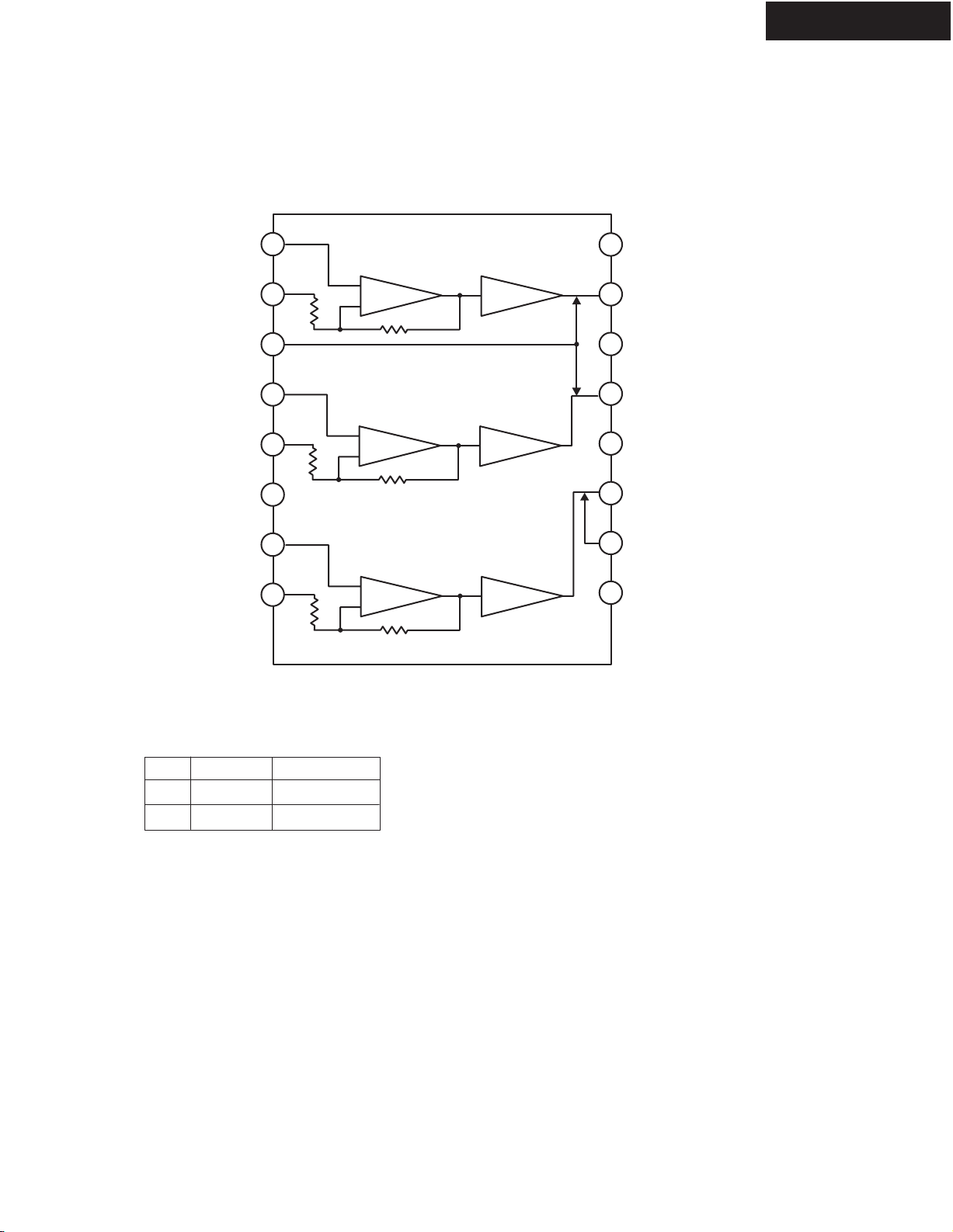
IC BLOCK DIAGRAMS AND TERMINAL DESCRIPTIONS-29
Q2106, 2107: LA7106M (6ch AMP + Driver)
BLOCK DIAGRAM
TX-SR603/603E/8360
VIN1+
NFB1
MUTE1
VIN2+
NFB2
-VCC1
VIN3+
NFB3
1
2
3
4
5
6
7
8
6dB DR
6dB DR
6dB DR
16
15
14
13
12
11
10
9
+VCC
VOUT1
GND
VOUT2
DR CTL
VOUT3
MUTE2
-VCC2
TRUTH TABLE
Pins 3 , 10
Throuth
H
L
Pins 12
150 ohm Driver
75 ohm DriveMute
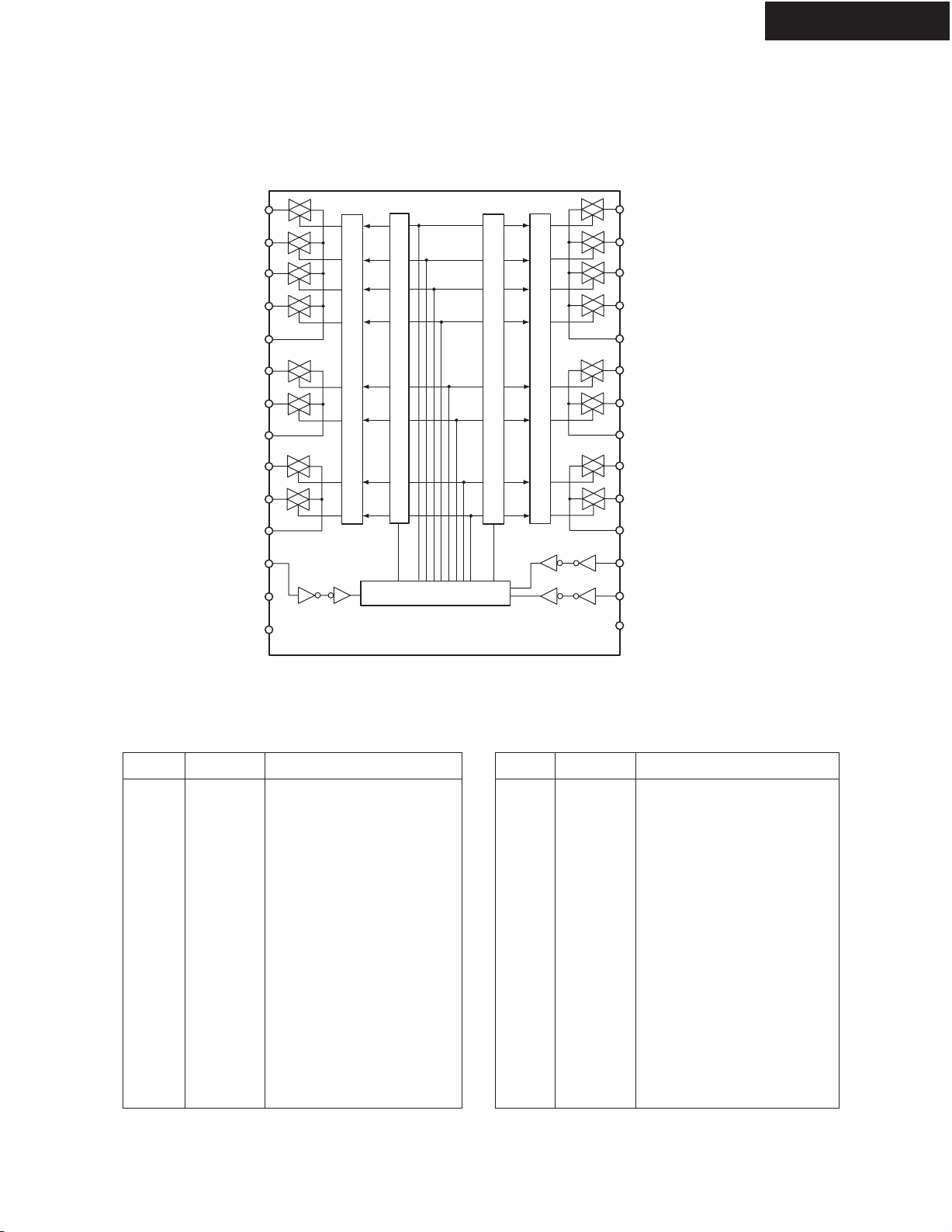
IC BLOCK DIAGRAMS AND TERMINAL DESCRIPTIONS-30
Q2111: NJU7313AM (Analog Function Switch)
BLOCK DIAGRAM
TX-SR603/603E/8360
L1
L2
L3
L4
L-COM1
L5
L6
L-COM2
L7
L8
L-COM3
ST
VDD
VEE
Level Shifter
Latch Circuit
Control Circuit
Latch Circuit
Level Shifter
R1
R2
R3
R4
R-COM1
R5
R6
R-COM2
R7
R8
R-COM3
DATA
CK
VSS
TERMINAL DESCRIPTION
Pin No. Pin Name Description
1
2
3
4
5
6
7
8
9
10
11
12
13
14
VEE
L1
L2
L3
L4
L-COM1
L5
L6
L-COM2
L7
L8
L-COM3
ST
VSS
Negative Voltage Supply
Analog switch input/output
Analog switch input/output
Analog switch input/output
Analog switch input/output
L1, L2, L3, L4 Common
Analog switch input/output
Analog switch input/output
L5, L6 common
Analog switch input/output
Analog switch input/output
L7, L8 Common
Chip enable
GND
Pin No. Pin Name Description
15
16
17
18
19
20
21
22
23
24
25
26
27
28
CK
DATA
R-COM3
R8
R7
R-COM2
R6
R5
R-COM1
R4
R3
R2
R1
VDD
Clock input
Data input
R7, R8 Common
Analog switch input/output
Analog switch input/output
R5, R6 Common
Analog switch input/output
Analog switch input/output
R1, R2, R3, R4 Common
Analog switch input/output
Analog switch input/output
Analog switch input/output
Analog switch input/output
Positive voltage supply
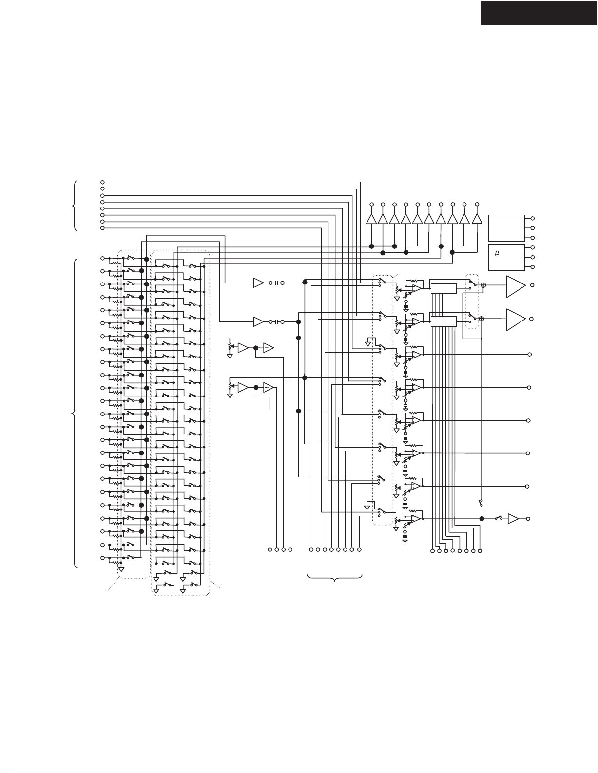
TX-SR603/603E/8360
IC BLOCK DIAGRAMS AND TERMINAL DESCRIPTIONS-31
Q5501: NJW1157(8-CHANNEL ELECTRONIC VOLUME WITH INPUT SELECTOR)-1/2
BLOCK DIAGRAM
Multi-Channel Input A
LAIN
RAIN
CAIN
LSAIN
RSAIN
LBAIN
RBAIN
SWAIN
L1IN
R1IN
L2IN
R2IN
L3IN
R3IN
L4IN
R4IN
L5IN
R5IN
L6IN
2 Channel Input
R6IN
L7IN
R7IN
L8IN
R8IN
L9IN
R9IN
L10IN
R10IN
L11IN
R11IN
L12IN
R12IN
Att Gain
Att Gain
DCLA1DCLA2
DCRA1DCRA2
FR+
FL-
FL+
FR-
LBIN
RBIN
CBIN
LSBIN
RBBIN
LBBIN
SWBIN
RBBIN
RECA1L
RECA1R
Volume
RECA2L
RECA3L
RECA2R
Multi-channel
Amp
Gain
FIL4_L
RECA3R
TONE
TONE
FIL3_L
RECB1L
RECB1R
FIL2_L
FIL1_L
RECB2L
BSW
FIL2_R
FIL3_R
FIL4_R
RECB2R
Supply
Voltage
COM
Interface
TSW
SSW
FIL1_R
SW
SW
V+
GND
VLATCH
DATA
CLOCK
LOUT
ROUT
COUT
LSOUT
RSOUT
LBOUT
RBOUT
SWOUT
Input Selector
REC Out Selector
Multi-Channel Input B

TX-SR603/603E/8360
IC BLOCK DIAGRAMS AND TERMINAL DESCRIPTIONS-32
Q5501: NJW1157(8-CHANNEL ELECTRONIC VOLUME WITH INPUT SELECTOR)-2/2
TERMINAL DESCRIPTON
No.
1
2
3
4
5
6
7
8
9
10
11
12
13
14
15
16
17
18
19
20
21
22
23
24
25
26
27
28
29
30
31
32
33
34
35
36
37
38
39
40
41
42
43
44
45
46
47
48
49
50
SYMBOL
LOUT
ROUT
COUT
LSOUT
RSOUT
LBOUT
RBOUT
SWOUT
DC_L1
DC_L2
FIL_BL
FIL_TL
DC_R1
DC_R2
FIL_BR
FIL_TR
N.C.
N.C.
V+
VREC_A1L
REC_A1R
REC_A2L
REC_A2R
REC_A3L
REC_A3R
REC_B1L
REC_B1R
REC_B2L
REC_B2R
DCCAP_L
DCCAP_R
DCCAP_C
GND
GND
DCCAP_LS
DCCAP_RS
DCCAP_LB
DCCAP_RB
DCCAP_SW
DCL_OUT
DCL_IN
DCR_OUT
DCR_IN
FL+
FLFR+
FRVDDOUT
VSSOUT
FUNCTION
Lch output
Rch output
Cch output
LSch output
RSch output
LBch output
RBch output
SWch output
Lch Bass filter DC cut capacitor output terminal
Lch Bass filter DC cut capacitor input terminal
Lch Bass filter terminal
Lch Treble filter terminal
Rch Bass filter DC cut capacitor output terminal
Rch Bass filter DC cut capacitor input terminal
Rch Bass filter terminal
Rch Treble filter terminal
No Connect
No Connect
+ Power supply voltage input
- Power supply voltage input
"Input selector" Lch REC output A1
"Input selector" Rch REC output A1
"Input selector" Lch REC output A2
"Input selector" Rch REC output A2
"Input selector" Lch REC output A3
"Input selector" Rch REC output A3
"Input selector" Lch REC output B1
"Input selector" Rch REC output B1
"Input selector" Lch REC output B2
"Input selector" Rch REC output B2
Switching noise rejection capacitor
Switching noise rejection capacitor
Switching noise rejection capacitor
Ground
Ground
Switching noise rejection capacitor
Switching noise rejection capacitor
Switching noise rejection capacitor
Switching noise rejection capacitor
Switching noise rejection capacitor
"Input selector" Lch output
"Multi-channel selector" Lch input
"Input selector" Rch output
"Multi-channel selector" Rch input
"Input selector gain control" Lch no-inverted output
"Input selector gain control" Lch inverted output
"Input selector gain control" Rch no-inverted output
"Input selector gain control" Rch inverted output
Internal Digital +Power Supply Output
Internal Digital -Power Supply Output
No.
51
52
53
54
55
56
57
58
59
60
61
62
63
64
65
66
67
68
69
70
71
72
73
74
75
76
77
78
79
80
81
82
83
84
85
86
87
88
89
90
91
92
93
94
95
96
97
98
99
100
SYMBOL
L1IN
R1IN
L2IN
R2IN
L3IN
R3IN
L4IN
R4IN
L5IN
R5IN
L6IN
R6IN
L7IN
R7IN
L8IN
R8IN
L9IN
R9IN
L10IN
R10IN
L11IN
R11IN
L12IN
R12IN
N.C.
DGND
DATA
CLOCK
LATCH
LAIN
RAIN
CAIN
LSAIN
RSAIN
LBAIN
RBAIN
SWAIN
LBIN
RBIN
CBIN
LSBIN
RSBIN
LBBIN
RBBIN
SWBIN
GND
GND
VSSOUT2
VDDOUT2
TCCAP
FUNCTION
"Input selector" Lch input 1
"Input selector" Rch input 1
"Input selector" Lch input 2
"Input selector" Rch input 2
"Input selector" Lch input 3
"Input selector" Rch input 3
"Input selector" Lch input 4
"Input selector" Rch input 4
"Input selector" Lch input 5
"Input selector" Rch input 5
"Input selector" Lch input 6
"Input selector" Rch input 6
"Input selector" Lch input 7
"Input selector" Rch input 7
"Input selector" Lch input 8
"Input selector" Rch input 8
"Input selector" Lch input 9
"Input selector" Rch input 9
"Input selector" Lch input 10
"Input selector" Rch input 10
"Input selector" Lch input 11
"Input selector" Rch input 11
"Input selector" Lch input 12
"Input selector" Rch input 12
No Connect
Digital Ground
Control data signal input
Clock signal input
Latch signal input
Multi-channel Lch input A
Multi-channel Rch input A
Multi-channel Cch input A
Multi-channel LSch input A
Multi-channel RSch input A
Multi-channel LBch input A
Multi-channel RBch input A
Multi-channel SWch input A
Multi-channel Lch input B
Multi-channel Rch input B
Multi-channel Cch input B
Multi-channel LSch input B
Multi-channel RSch input B
Multi-channel LBch input B
Multi-channel RBch input B
Multi-channel SWch input B
Ground
Ground
Internal Digital -Power Supply Output 2
Internal Digital +Power Supply Output 2
Switching noise rejection capacitor
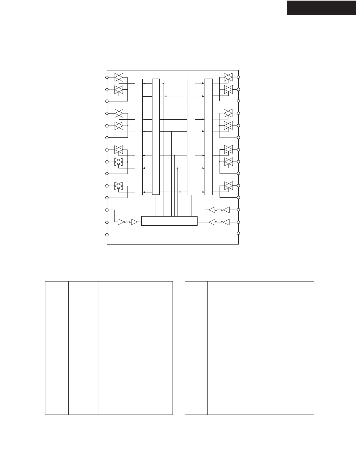
IC BLOCK DIAGRAMS AND TERMINAL DESCRIPTIONS-33
Q5502: NJU7311AM (Analog Function Switch)
BLOCK DIAGRAM
TX-SR603/603E/8360
L1
L2
L-COM1
L3
L4
L-COM2
L5
L6
L-COM3
L7
L-COM4
ST
VDD
VEE
Level Shifter
Latch Circuit
Control Circuit
Latch Circuit
Level Shifter
R1
R2
R-COM1
R3
R4
R-COM2
R5
R6
R-COM3
R7
R-COM4
DATA
CK
VSS
TERMINAL DESCRIPTION
Pin No. Pin Name Description
1
2
3
4
5
6
7
8
9
10
11
12
13
14
VEE
L1
L2
L-COM1
L3
L4
L-COM2
L5
L6
L-COM3
L7
L-COM4
ST
VSS
Negative Voltage Supply
Analog switch input/output
Analog switch input/output
L1, L2, Common
Analog switch input/output
Analog switch input/output
L3, L4 common
Analog switch input/output
Analog switch input/output
L5, L6 Common
Analog switch input/output
L7 Common
Chip enable
GND
Pin No. Pin Name Description
15
16
17
18
19
20
21
22
23
24
25
26
27
28
CK
DATA
R-COM4
R7
R-COM3
R6
R5
R-COM2
R4
R3
R-COM1
R2
R1
VDD
Clock input
Data input
R7 Common
Analog switch input/output
R5, R6 Common
Analog switch input/output
Analog switch input/output
R3, R4 Common
Analog switch input/output
Analog switch input/output
R1, R2, Common
Analog switch input/output
Analog switch input/output
Positive voltage supply

IC BLOCK DIAGRAMS AND TERMINAL DESCRIPTIONS-34
Q5640: AN34060A (3 Output Voltage Regulator)
BLOCK DIAGRAM
TX-SR603/603E/8360
Peak Current
Protection &
Thermal Protection
Pre
Drive
Reference Voltage
1
3
2
TERMINAL DESCRIPTION
Pin No.
1
2
3
4
5
6
7
Description
MODE 1
REG 1
VCC
GND
REG 2
VCC
REG 3
Function
WHEN MODE 1 pin is 5V, REG 1 output is "H".
WHEN MODE 1 pin is "H", REG 1 output is 5.0V (Io1(peak) = 300mA min).
Connected to Power supply
Connected to IC substrate
WHEN MODE 1 pin is "H", REG 2 output is 3.3V (Io2(peak) = 200mA min).
Connected to Power supply
WHEN MODE 1 pin is "H", REG 3 output is 2.5V (I
VCC
Output
VCC
Pre
Drive
6
5
4
o3(peak) = 600mA min).
VCC
Pre
Drive
7

FL TUBE VIEW
Q801: 16BT127GNK
TX-SR603/603E/8360
16G
15G 14G 13G 12G 11G 10G 9G
1-3 2-3 3-3 4-3 5-3
1-4 2-4 3-4 4-4 5-4
1-5 2-5 3-5 4-5 5-5
1-6 2-6 3-6 4-6 5-6
1-7 2-7 3-7 4-7 5-7
16G
P1
P2
P3
P4
P5
P6
P7
P8
P9
P10
P11
P12
P13
P14
P15
P16
P17
P18
15G-1G
8G 7G 6G 5G 4G 3G 2G 1G
1-1
2-1 3-1 4-1 5-1
1-2 2-2 3-2 4-2 5-2
(1G-15G)
1-1
2-1
3-1
4-1
5-1
1-2
2-2
3-2
4-2
5-2
1-3
2-3
3-3
4-3
5-3
1-4
2-4
3-4
P19
P20
P21
P22
P23
P24
P25
P26
P27
P28
P29
P30
P31
P32
P33
P34
P35
16G
-
15G-1G
4-4
5-4
1-5
2-5
3-5
4-5
5-5
1-6
2-6
3-6
4-6
5-6
1-7
2-7
3-7
4-7
5-7
MICROPROCESSOR TERMINAL DESCRIPTIONS-1
Q701: M30624MHP-253FPU0
TX-SR603/603E/8360
Pin No. Pin name I/O Description
1
2
3
4
5
6
7
8
9
10
11
12
13
14
15
16
17
18
19
20
21
22
23
24
25
26
27
28
29
30
31
32
33
34
35
36
37
38
39
40
41
42
43
44
45
46
47
48
49
50
FLDSDO
FLDCLK
FLDCS
FLDRST
FSWSDO
FSWSTB
FSWCLK
BYTE
CNVSS
SDET
SYNC
RESET
XOUT
VSS
XIN
VCC1
NU
VSUNC
REMIN
POFF
DIRINT1
DIRINT0
DIRCS
DIRRST
DSPFCS
DSPCS
VMUT
VCRST
SCL
SDA
FTXD
FRXD
FCLK
FBUSY
DIGSDO
DIGSDI
DIGCLK
DSPBUSY
DSPINT
DSPFINT
FEPM
DSPRST
VOLSTB
VOLCLK
VOLDAT
FCE
Z2MUT
SBZ2MUT
AMUT
SPRLB
I/O
---
---
---
---
---
---
---
Act.
O
O
CLK
O
O
O
O
O
I
I
I
I
I
I
I
I
O
O
O
O
O
O
O
O
I
O
CLK
O
O
I
O
CLK
I
I
I
O
O
O
O
CLK
O
I
O
O
O
O
Output serial data for control of FL driver IC/ OSD IC.
H
Output serial clock for control of FL driver IC/ OSD IC.
Output chip select for FL driver IC.
H
Output reset signal for FL driver IC.
L
Output serial data for control of function switch (NJU7311).
H
Output strobe for control of function switch (NJU7311).
H
Output serial clock for control of function switch (NJU7311).
H
Select of external bus width. Connect to ground.
--Select of processor mode.
--Input signal of detection of S video signal.
L
Input signal of detection of synchronizing signal.
L
Input signal for system reset.
L
Connected to oscillator.
--Ground.
--Connected to oscillator.
--Power supply.
--Not used.
--Input signal of detection of vertical synchronizing signal.
L
Input signal from remote sensor.
L
Input signal of power failure detection.
H
Not used.
H
Input signal of interrupt request detection of DSP C.
H
Output signal for chip select of DIR/CODEC.
L
Output signal for reset of DIR/CODEC.
L
Output signal for chip select of DSP A/B.
L
Output signal for chip select of DSP C.
L
Output control signal for video mute.
L
Output reset signal for video decoder/ encoder IC.
L
Output serial clock for video decoder/ encoder IC.
L
Output serial data for video decoder/ encoder IC.
H
For writing of flash microprocessor.
H
For writing of flash microprocessor.
H
For writing of flash microprocessor.
Output reset signal for DSPIC.
H
Output signal for serial communications with DIR/ CODEC/DSP IC.
H
Input signal for serial communications with DIR/ CODEC/DSP IC.
H
Output clock for serial communications with DIR/ CODEC/DSP IC.
Input signal of detect busy signal of DSP C.
H
Input signal of detect interrupt request signal of DSP C.
L
Input signal of detect interrupt request signal of DSP AB.
L
For writing of flash microprocessor.
H
Output reset signal for DSP IC.
L
Output strobe for control of volume IC.
H
Output serial clock for control of volume IC.
Output serial data for control of volume IC.
H
For writing of flash microprocessor.
H
Output signal of zone 2 mute
H
Output signal of surround back mute.
H
Output signal of audio mute.
H
Output control signal for relay drive of speakers-B.
H

MICROPROCESSOR TERMINAL DESCRIPTIONS-2
Q701: M30624MHP-253FPU0
TX-SR603/603E/8360
Pin No. Pin name I/O Description
51
52
53
54
55
56
57
58
59
60
61
62
63
64
65
66
67
68
69
70
71
72
73
74
75
76
77
78
79
80
81
82
83
84
85
86
87
88
89
90
91
92
93
94
95
96
97
98
99
100
SPRLSB
SPRLCS
SPRLF
TUMUT
PLLCE
PLLSDO
PLLCLK
STEREO/PLLSDI
SD
VPOWER
APOWER
VCC2
SEC1H
VSS
VOLH
THERMAL
PROTECT
FANCTRL
FANH
TRGZ2
RDSDAT
RDSSIG
SYSIN
NU
~RDSCLK
~SYSOUT
LEDPURE
LEDZONE2
LEDSTBY
HPRL
HPDET
MICDET
VOLB
VOLA
INIT3
INIT2
INIT1
BAND
KEYINT3
KEYINT2
KEYINT1
KEYINT0
KEY3
KEY2
KEY1
AVSS
KEY0
VREF
AVCC
OSDCS
---
---
---
---
---
---
Act.
O
O
O
O
O
O
O
I
I
O
O
O
I
I
I
O
O
O
I
I
I
I
O
O
O
O
O
I
I
I
I
I
I
I
I
I
I
I
I
I
I
I
I
O
H
H
H
H
H
H
CLK
L
L
H
H
--H
---
A/D
A/D
H
L
L
H
H
H
H
--L
L
H
H
L
H
H
L
H
H
A/D
A/D
A/D
A/D
L
L
L
L
A/D
A/D
A/D
---
A/D
---
--H
Output control signal for relay drive of surround back speakers.
Output control signal for relay drive of center and surround speakers.
Output control signal for relay drive of front speakers.
Output signal of tuner mute.
Output chip enable for PLL IC of tuner.
Output serial data for PLL IC of tuner.
Output serial clock for PLL IC of tuner.
Input detection of stereo signal, and serial data of PLL IC.
Input detection signal of demodulation of tuner.
Output control signal of power supply of the video circuit.
Output control signal of main power supply.
Power supply.
Output control signal for power supply of amplifier section.
Ground.
Input detection signal of speaker output level.
Input detection signal of thermal detection.
Input detection signal of over current of speaker output.
Output control signal of cooling fan. Function control.
Output control signal of cooling fan. Speed control.
Output of 12V trigger out/ zone 2 signal.
Input serial data of RDS. MPP (European model) only.
Input detection signal of demodulation of RDS. MPP (European model) only.
Input signal of RI (system control).
Not used.
Input serial clock of RDS. MPP (European model) only.
Output signal of RI (system control).
Output control signal of pure audio LED. Except MDD (USA model).
Output control signal of zone 2 LED
Output control signal of Standby LED.
Output control signal for relay drive of headphone.
Input detection signal of headphone state.
Input detection signal of setup mic state.
Input signal of rotary encoder.
Input signal of rotary encoder.
For initial setting-3.
For initial setting-2.
For initial setting-1.
For initial setting of tuner band and step.
Input signal of operation keys.
Input signal of operation keys.
Input signal of operation keys.
Input signal of operation keys.
Input signal of operation keys.
Input signal of operation keys.
Input signal of operation keys.
Ground for A/D.
Input signal of operation keys.
Power supply for reference of A/D.
Power supply.
Output of chip select of OSD IC.

ADJUSTMENT PROCEDURE-1
IDLING CURRENT ADJUSTMENT
[When]
Exchange Power transistor (Q6051 - Q6066) and Amplifier PC board (NAAF-8523).
[Procedure]
<Note> No load and No signal
Refer to <Fig-1> in " ADJUSTMENT PROCEDURES-2 " about the adjustment points and the test points.
1. Before idling adjustment, turn the trimming resistors to counter clockwise.
2. Connect the DC voltmeter to test points.
Connect 100 ohm resistance near the terminal of the two poles of a Jig terminal.
TX-SR603/603E/8360
DC voltmeter
3. Connect the AC power cord to wall outlet.
4. Press the STANDBY/ON button into the power on.
5. Adjust the trimming resistors as following procedure immediately after power on.
Channel
Left
Right
Center
Surround Left
Surround Right
Surround Back Left
Surround Back Right
6. Wait for 4 - 6 minutes. (Heat running)
7. Re-adjust the trimming resistors as following procedure.
Channel
Left, Right and
Center
Surround Left
Surround Right
Surround Back Left
Surround Back Right
100 ohms
1/4watts
Mark
L
R
C
SL
SR
SBL
SBR
Adjustment point
R6040, R6041 and
R6042
R6043, R6044,
R6045 and R6046
Adjustment point
(Trimming resistor)
R6040
R6041
R6042
R6043
R6044
R6045
R6046
Jig terminal
Measuring point
(Test point)
P6080
P6081
P6082
P6083
P6084
P6085
P6086
Measured value
In case below 9 mV
In case 9 - 11 mV
In case over 11 mV
In case below 6 mV
In case 6 - 8 mV
In case over 8 mV
Test point
ID+
ID-
Adjustment value
2.5 mV
2.5 mV
2.5 mV
1.5 mV
1.5 mV
1.5 mV
1.5 mV
Adjustment value
9 mV
Leave it as it is
11 mV
6 mV
Leave it as it is
8 mV
Specifications
( In a stable state)
12 +/- 3 mV
9 +/- 3 mV
8. Disconnect the DC voltmeter.
9. Press the STANDBY/ON button into the power off.
10. Disconnect the AC power cord.
Idling current are stabilized in about
10 minutes after a power supply ON.
 Loading...