

Page 1
SERVICE MANUAL
SERVICE MANUAL
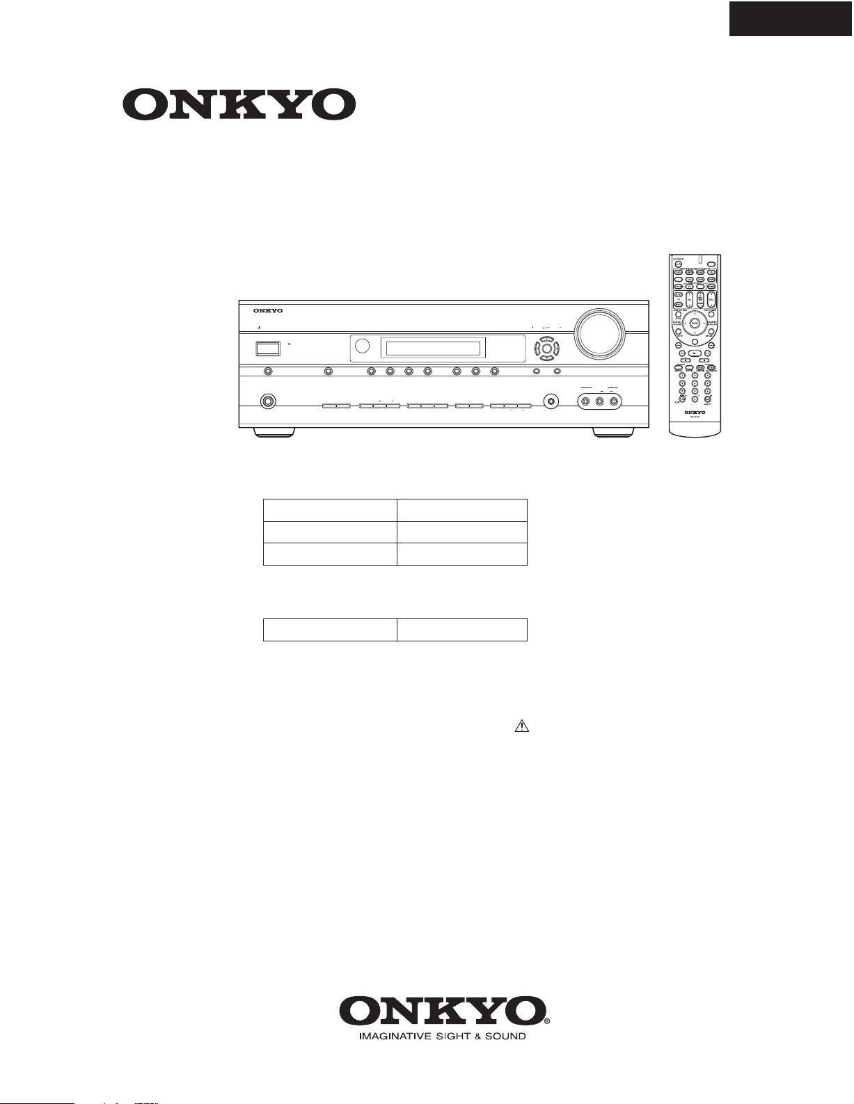
7.1-CH HOME THEATER RECEIVER
HT-R560
Ref. No. 4066
042008
ON/STANDBY
DOCK
PHONES
MODEL
STANDBY
MULTI CH
DVD TAPE
TONE
SPEAKERS
BA
HT-R560
CD
AUXCBL/SATVCR/DVR
MOVIE/TV MUSIC GAME
TUNER
DISPLAY
DIGITAL INPUT
DIMMER
TUNING PRESET
ENTER
SETUP
RETURN
SETUP MIC
MEMORY
TUNING MODE
CLEAR
AUX INPUT
L AUDIO R
VIDEO
AV RECEIVER
HT-R560 for HT-S5100 Black and Silver models
(HT-S5100 : 7.1ch Home Theater System)
B MDD
B MDC, S MDC
B MPP
120V AC, 60Hz
120V AC, 60Hz
230V AC, 50Hz
HT-R560 for AVX-760LD Black model
(AVX-760LD : 5.1ch Home Theater System)
120V AC, 60HzB MDD
MASTER VOLUME
HT-R560
MULTI CH
RECEIVER
AUDIO
LISTENING MODE
MOVIE/TV
MUSIC
DIMMER
RC-707M
DISPLAY
SAFETY-RELATED COMPONENT
WARNING!!
COMPONENTS IDENTIFIED BY MARK ON THE
SCHEMATIC DIAGRAM AND IN THE PARTS LIST ARE
CRITICAL FOR RISK OF FIRE AND ELECTRIC SHOCK.
REPLACE THESE COMPONENTS WITH ONKYO
PARTS WHOSE PART NUMBERS APPEAR AS SHOWN
IN THIS MANUAL.
MAKE LEAKAGE-CURRENT OR RESISTANCE
MEASUREMENTS TO DETERMINE THAT EXPOSED
PARTS ARE ACCEPTABLY INSULATED FROM THE
SUPPLY CIRCUIT BEFORE RETURNING THE
APPLIANCE TO THE CUSTOMER.
Page 2
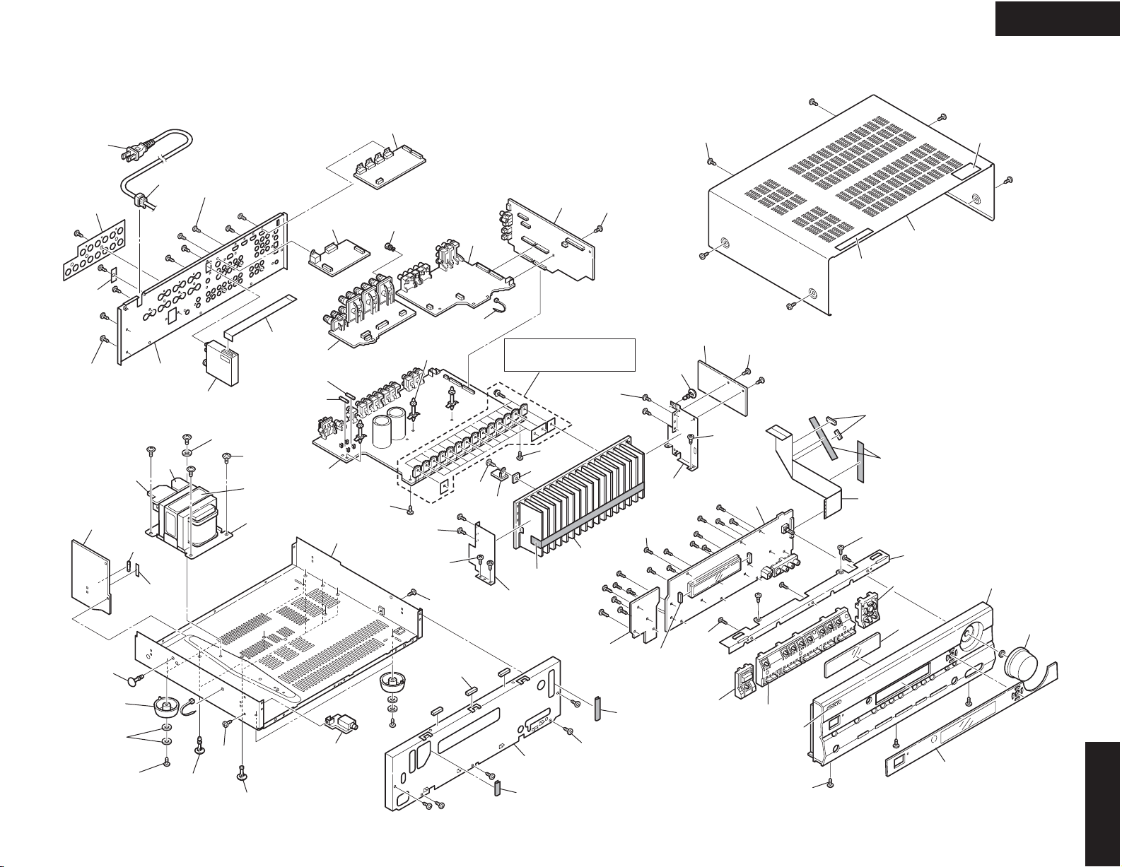
EXPLODED VIEWS-1
P901
A096
MDD, MDC Type : 7 pcs.
MPP Type : 6 pcs.
U45
A031
U02
A030
x 4 pcs.
A033
T901
A103
A104
A097
x 30 pcs.
U12
A035
A037
A093
U13
F901
F901C
<PP> Type only
P101
U37
F6902
F6901
U01
U31
A072
U42
MPP Type only
P6601A
x 14 pcs.
A047
A018
x 3 pcs.
A043
x 2 pcs.
A044
x 2 pcs.
A044
A071
x 3 pcs.
U36
A013
x 8 pcs.
A048
U03
U30
A052
Refer to
EXPLODED VIEWS-2
A043
x 2 pcs.
A047
U04
A040
A039
A041
U11
A022
A042
A011
x 18 pcs.
A050
A061
x 6 pcs.
U17
A012
x 3 pcs.
A046
x 2 pcs.
A044
U10
A060
A109
MDD, MDC Type only
A062
x 2 pcs.
A039
x 2 pcs.
P701
A005
x 2 pcs.
A004
A074
A003
HT-R560
A102
A073
A055
A066
x 4 pcs.
A068
x 8 pcs.
A067
x 4 pcs.
A016
A020
x 2 pcs.
A021
x 5 pcs.
U14
A001
A039
A002
x 5 pcs.
A039
A076
A075
A077
A089
x 3 pcs.
A083
HT-R560
Page 3
EXPLODED VIEWS-2
HT-R560
Q6050B
x 6 pcs.
A049
x 14 pcs.
Q6056
Q6066
Q6055
Q6065
Q6054
Q6064
Q6053
Q6063
Q6052
Q6062
Q6051
Q6061
Q6050
Q6050A
x 2 pcs.
Q6060
HT-R560
Page 4
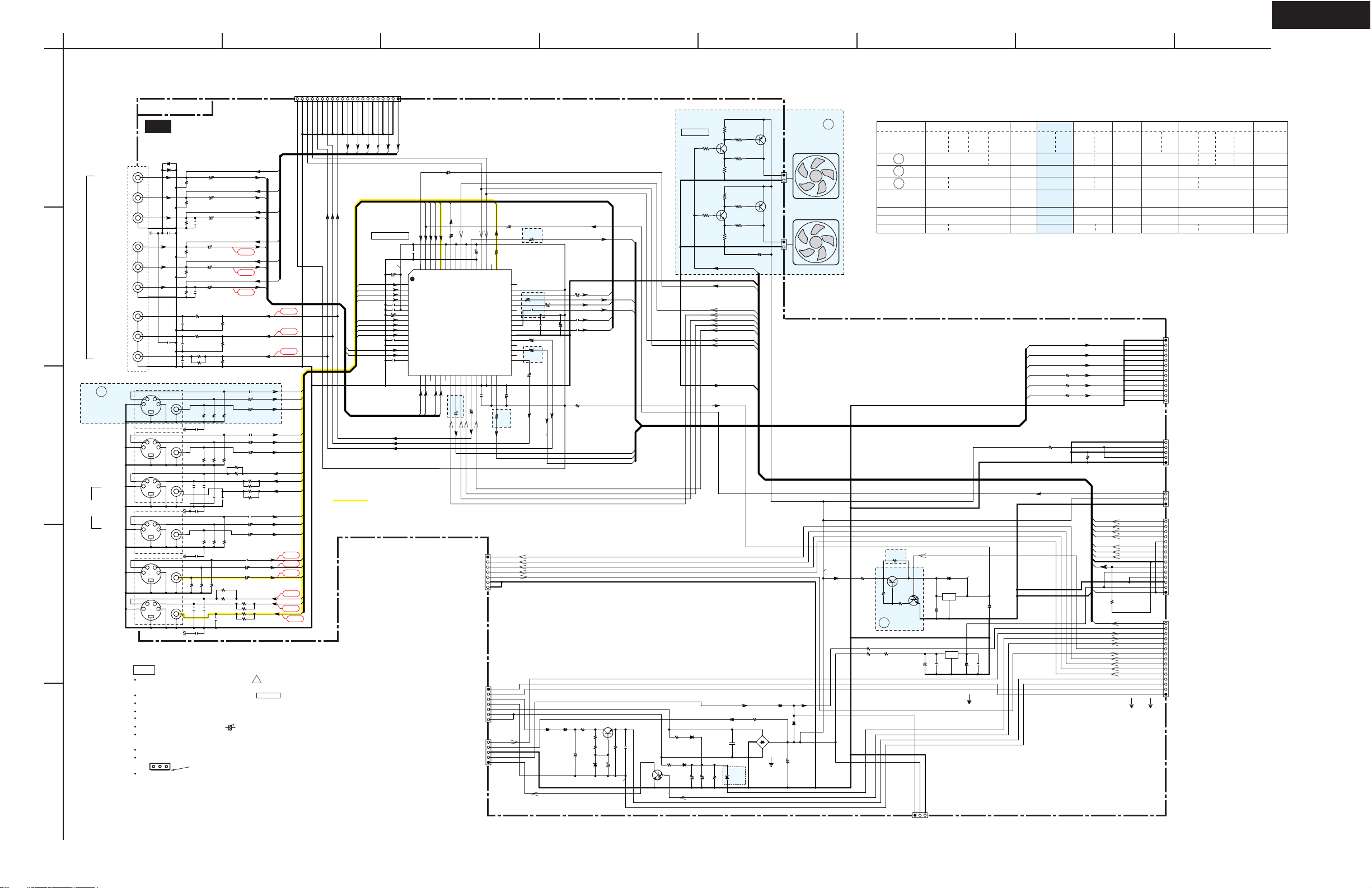
HT-R560
A
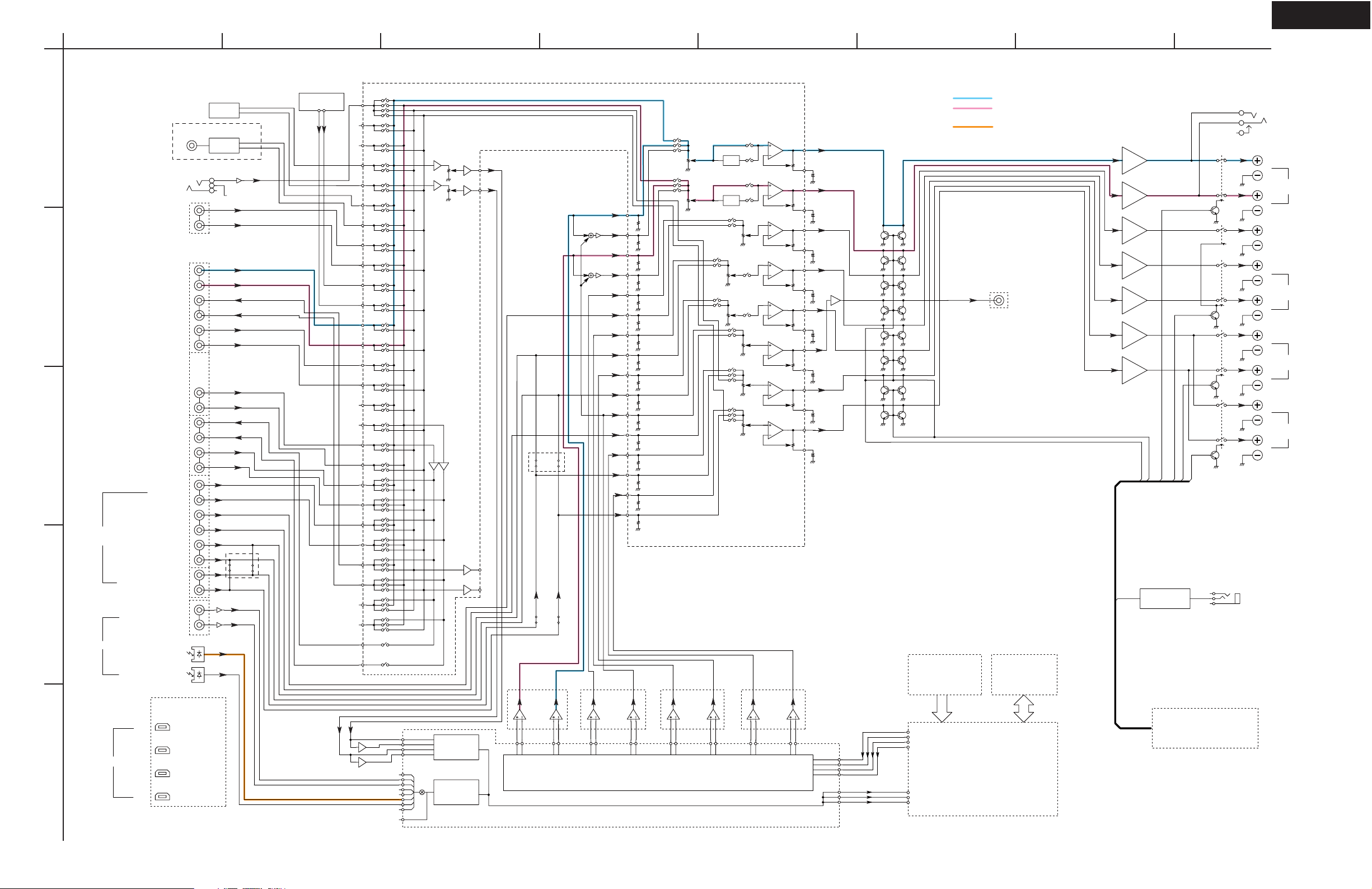
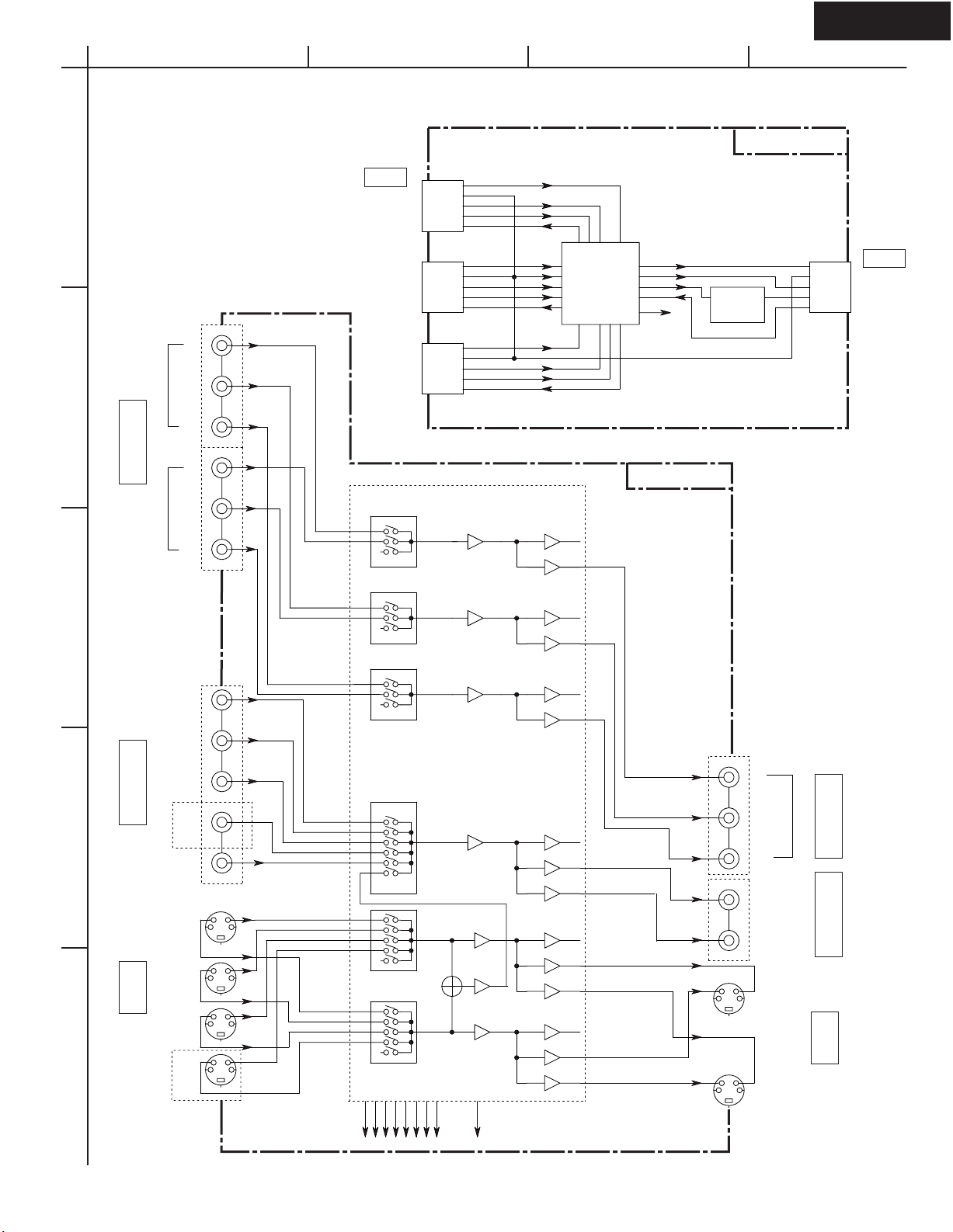
BLOCK DIAGRAMS-1
AUDIO SECTION
1
SETUP MIC
(FRONT IN)
2
TAPE OUT
CBL/SAT IN
VCR/DVR OUT
3
VCR/DVR IN
DVD
(MULTI IN)
SUBWOOFER
SURROUND
SURROUND BACK
4
COAXIAL
DIGITAL IN
OPTICAL
IN1
IN2
5
HDMI
IN3
OUT
MDD. MDC Type only
AUX IN
CD IN
TAPE IN
FRONT
CENTER
1
(DVD)
2
(CBL/SAT)
1
(VCR/DVR)
2
(CD)
Refer to
BLOCK DIAGRAMS-2
BCDEFGH
Q5501
DOCK
SIRIUS
MIC AMP.
MICDET
TUNER UNIT
L
R
L
R
L
R
L
R
L
R
L
R
L
R
L
R
L
R
L
NC
R
40
57
MAIN L
58
63
64
65
66
61
62
59
60
55
56
53
54
51
52
49
50
47
48
45
46
71
72
69
70
67
68
-
-
MAIN R
SUB R
SUB L
36
37
74
INVERTING
INVERTING
25k25k
35
73
25k25k
34
75
25k
30
25k25k
78
33
25k25k25k
77
32
76
25k
31
25k25k25k25k25k
80
NC
29
REC R
REC L
38
39
LPF
Q401
NJM45800-D
FL
32
33
FR
16
15
14
13
49
43
42
44
46
45
48
47
50
2ch ADC
DIR
31
30
79
28
C
37
36
LPF
Q402
NJM45800-D
SW
34
35
28
8ch DAC
Q301
CS42518
R2S15211FP
SELECTOR / TONE / VOLUME
TONE
TONE
SL
29
LPF
Q403
NJM45800-D
SR
27
26
22
SBL
23
LPF
Q404
NJM45800-D
21
SBR
FL
19
20
+
FR
17
18
C
7
6
+++++
SL
14
15
SR
12
11
SW
9
10
SBL
4
5
+
SBR
2
1
+
20
62
63
64
1
61
60
54
Q5606
Q5605
Q5607
Q5600
Q5604
Q5603
Q5602
Q5601
NC
NC
NC
Q5610
NC
NC
NC
NC
ES29LV160ET-70TG
FLASH MEMORY
(DSP ROM)
117
116
115
113
139
141
120
Q282
D788E001BRFP266
AUDIO ANALOG
FRONT L
FRONT R
AUDIO DIGITAL
M12L64164A-7TG
Q201
DSP
PREOUT
SUBWOOFER
Q281
SDRAM
POWER AMPLIFIER
+29dB
+29dB
+29dB
+29dB
+29dB
+29dB
+29dB
AMUT
SBMUT
INTERFACE
RL6600
Q6601
RL6602
RL6603
Q6602
RL6604
Q6603
RL6607
Q6604
FRL
Z2RL
SBRL
CSRL
RI
Q701
M30626FHPFP
MAIN MICROPROCESSOR
PHONES
L
SPEAKERS A
R
CENTER
SPEAKER
L
SURROUND
SPEAKERS
R
L
SURROUND BACK
SPEAKERS
R
L
FRONT
SPEAKERS B
R
RI
FRONT
Page 5
HT-R560
A
BLOCK DIAGRAMS-2
VIDEO / HDMI SECTION
1
Y
IN 1
2
COMPONENT
CB
CR
Y
VIDEO INPUT
IN 2
CB
CR
BCD
NAHDM-9475
HDMI
IN 3
HP DET
IN 2
HP DET
IN 1
HP DET
PY
TMDS3
TMDS
CEC
CEC
DDC3
DDC
RPWR3
+5V
HPD3
TMDS2 TMDS
TMDS
CEC
CEC
DDC2
DDC
RPWR2
+5V
HPD2
TMDS1
TMDS
CEC
CEC
DDC1
DDC
RPWR1
+5V
HPD1
Q3001
AN15880A-VT
VIDEO SWITCH
6dB
HDMI SWITCH
DRV
DRV
Q8001
TMDS341A
DDC
RPWR
HPD
I2C
NAVD-9467
+5V Reg
TMDS
CEC
DDC
+5V
HP DET
HDMI
OUT
3
DVD
PB
6dB
PR
6dB
DRV
DRV
DRV
DRV
VCR/DVR
CBL/SAT
COMPOSITE
VIDEO INPUT
4
NC
AUX
(FRONT)
C
DVD
VCR/DVR
INPUT
S VIDEO
CBL/SAT
5
NC
Y
YC
YC
C
Y
S2
S1
S3S4S5
CV
SY
SC
S6
S7
4/6dB
4/6dB
6dB
4/6dB
S8
MUTE
DRV
DRV
DRV
DRV
DRV
DRV
DRV
DRV
DRV
Y
CB
COMPONENT
CR
VIDEO OUTPUT
MONITOR
VCR/DVR
C
Y
COMPOSITE
VIDEO OUTPUT
MONITOR
S VIDEO
OUTPUT
Y
C
VCR/DVR
Page 6
HT-R560
A
SCHEMATIC DIAGRAMS-1 (SD-1)
AUDIO INPUT SECTION
1
RI
P7900
NC
P7901
R
TUNER
L
P7902
R
CD IN
L
2
R
OUT
L
TAPE
R
IN
L
3
P7904
OUT
FRONT
CENTER
LIST
BACK
R
L
R
L
R
IN
L
P7905
R
L
R
L
P7906
R
L
CBL/SAT IN
VCR/DVR
4
SURROUND
DVD
(MULTI IN)
5
SUBWOOFER
D
SURROUND
P5505
R5519
R5520
R5521
R5522
R5523
R5524
R5525
R5526
R5501
R5502
R5503
R5504
R5505
R5506
R5507
R5508
R5513
R5514
R5515
2.2K
R5516
2.2K
R5517
330
R5518
330
330
330
330
330
330
330
330
330
R5500
330
330
330
330
2.2K
2.2K
330
330
330
330
330
R5541
220K
R5542
220K
R5543
220K
R5544
220K
R5545
220K
R5546
220K
R5547
220K
R5548
220K
R5553
220K
R5554
220K
R5555
220K
R5556
220K
R5557
220K
R5558
220K
R5559
220K
R5560
220K
R5561
220K
R5562
220K
R5563
220K
R5564
220K
R5565
220K
R5566
220K
MICROPROCESSOR PCB
To NADG-
9457 SD-3 : A3
P304
C5501
221J
C5502
221J
C5503
221K
C5504
221K
C5505
NC
C5506
NC
C5507
221J
C5508
221J
C5513
221J
C5514
221J
C5515
NC
C5516
NC
C5517
221J
C5518
221J
D5704
221J
C5704
D5714
C5519
221K
C5520
221K
C5521
221J
C5522
221J
D5705
C5705 221J
D5715
C5523
221J
C5524
221K
C5525
221J
C5526
221J
D5706
C5706 221J
D5716
BCDEFGH
CIN1
1-C : 1
CIN2
C5569
47/50
76
SWIN1
SBRIN2
29
77
SLIN1
SBLIN2
28
1
10K
10K
10K
7
P302
1
23456
DAC_FL
DAC_FR
79
78
SRIN1
SBLIN1
2-OUT
2-C
3-C
3-OUT
AGND
4-OUT
4-C
5-C
5-OUT
AGND
6-OUT
6-C
FLC
FLOUT
AGND
FROUT
FRC
TRE_R
BASS_R225BASS_R1
27
26
C5564 223J
C5563 823J
Q5503 : NJM4580
4
10K
8
MICROPROCESSOR PCB
To NADG-9457
SD-3 : A2
789
10
111213
-15VA
+15VA
DAC_C
GND_A
GND_D
DAC_SW
R5691
R5692
R5693
R5694
R5695
80
SBRIN1
10
11
12
13
14
15
16
17
18
19
22
C5562
R5586
3
2
5
6
1
2
3
4
5
6
7
8
9
20
21
23
24
1.8K
-6.8V
220K
220K
220K
220K
220K
C5551 47/25
C5552
C5553
C5554
C5555
C5556
C5557
C5558
C5559
C5560 823J
C5561
223J
+6.8V
474J
C5674
C5675
R5591
10K
R5592
R5593
470
1.2K
R5596
R5597
1.2K
470
R5599
10K
47/25
47/25
47/25
47/25
47/25
47/25
47/25
474J
470/16
470/16
!
VOL_CLK
PROTECT
VOL_DATA
R5585
1.8K
D5671
UDZ6.2C
D5673
D5672
UDZ6.2C
D5674
-14.8V
DAC_FR
DAC_FL
+14.8V
VOLH
SEC1H
SBR_OUT
SBL_OUT
C_OUT
SW_OUT1
SR_OUT
SL_OUT
R_OUT
L_OUT
R5674
(1W)
68
1SS133
R5675
68
(1W)
1SS133
14
AMUT
15
Z2_MUT
R5684
68
R5683
68
22
R5667
C5667
C5666
R5666
22
(1W)
(1W)
220/25
220/25
+15V
C5630
47/50
Subwoofer
+15V
D5709
D5719
-15V
-14.8V
R5630
220
R5631
+14.8V
3
C5672
RL1N4003
C5673
RL1N4003
3O2
Q5630 : NJM4580
221J
C5631
47K
15K
R5632
Q5670
78M15
1
I
O
G
2
C5670
220/25
C5671
220/25
1
G
I
Q5671
79M15
LIST
LIST
J5246
R5677
-23.5V
NC
P301
Z2_MUTE
SB_MUTE
NC
U01
AMPLIFIER PC BOARD
+15V
R5680
LIST
R5681
220K
R5682
LIST
LIST
SW_OUT
SBR_OUT
SBL_OUT
SR_OUT
SL_OUT
R_OUT
L_OUT
C_OUT
Z2_R
Z2_L
MUTING
D
LIST
C5601
47/50
C5602
47/50
C5600
100/25
C5603
47/50
C5604
47/50
C5605
47/50
C5606
47/50
C5607
47/50
47/50
C5608
C5609
R5601
R5602
47/50
4
Q5630A
3
1
2
R5634
10K
C5632
103J
1.2K
R5633
5
Q5630B
7
6
8
10/50
10/50
LIST
J5247
R5678
R5813
R5600
220K
220K
R5603
R5604
R5605
R5606
R5607
R5608
R5609
R5610
220K
R5611
LIST
R5612
LIST
220K
R5613
2.2K
R5614
220K
220K
2.2K
R5615
R5616
220K
220K
2.2K
R5617
2.2K
R5618
220K
220K
2.2K
R5619
LIST
270
2.2K
2.2K
+3.7V
LIST
R5814
Q5600
Q5601
Q5602
Q5603
Q5604
Q5605
Q5606
Q5607
Q5608
Q5609
LIST
A
R5620
R5621
LIST
R5622
LIST
R5623
R5624
R5625
R5626
R5627
100
0
0
0
0
0
Q5600 - 5610 : RN1441
Q5610
Q5611
NC
Q5612
NC
Q5613
NC
Q5614
NC
Q5615
NC
Q5616
NC
Q5617
NC
+22V
R5688
NC
R5686
NC
R5672
10
R5670
10
R5673
27
R5671
27
R5685
R5687
NC
+22V
2W
2W
2W
-22V
2W
NC
D9001 -6004 : RL1N4003
C9003
C9004
D9002
1000/35
1000/35
D9001
D9003D9004
C9001
R5660
2.2
334J
R5661
2.2
GND_S1
1W
1W
SD-2 : B3
+22V
S1L+
GND
SD-2 : B5
To NAAF-9419(2/2)
S1L-
NAAF-9419(1/2)
VOLH
SEC1H
PROTECT
Refer to following table about the parts displayed by mark " LIST ".
TA20 : Jumper wire L=20 mm
MODEL No.
A
B
C
Yes
Yes
Yes
D
R5680, 5682 220K None
R5813
R5814
R5611, 5612
R5621, 5622
R5677, 5678
J5246, 5247
Q5700
R5668
RL5700
AUDIO ANALOG SIGNAL
<Note>
1. NC = No mount of parts.
2. SD-x : XY is short for Schematic Diagrams-x and each sockets location, X = A to H, Y = 1 to 5.
D5700
C5700
FRONT L
FRONT R
2.2K
TA20
NC
0
0
P6991
AMPLIFIER PCB
To NAAF-9419(2/2)
SD-2 : B3
HT-R518 HT-R560 TX-SR576TX-SR506
None
None
Yes
None
None
None
None Yes YesYesYes Yes
None
0 0NoneNone None
2.2K 2.2K2.2K2.2K
None
None
15 (2W) 15 (2W) 15 (2W)None None
SP TERMINAL PCB
To NATRM-9468
R5567
C5527
221J
2.2K
C5528
R5568
221J
2.2K
C5529
R5569
R5570
C5530
D5717
D5707
1SS352
1SS352
C5531
R5571
221J
NC
C5532
R5572
R5573
C5533
C5534
R5574
D5708
D5718
1SS352
1SS352
Yes
Yes
0None None None
TA20NoneNone None
5
4
103J
C6086
3
2
1
SD-5 : H3
C6087
JL6604A
R5527
330
R5528
330
R5529
R5530
C5707
103K
R5531
100
R5532
R5533
R5534
C5708
103K
SBR
SBL
SR
SL
R
L
C
HT-R667
HT-R960
None
None
YesYes
Yes
None
None
None
None220K
None
0
15 (2W)
None
P6602
(Lever type)
GND_E
102J
C6076
103J
102J
C6077
R
P7907
R
ZONE 2
LINE OUT
L
NC
P7908
PRE OUT
SUBWOOFER
NC
To NAAF-9419(2/2)
SD-2 : E4
000 0
SPEAKERS B
L
LIST
C
B
FRONT
LIST
SIRIUS / DOCK TERMINAL PCB
To NARF-9458
SD-8 : E1
JL5502A
1
2345678
XM_L
iPOD_R
iPOD_L
R5580
R5582
XM_R
220K
R5581
220K
GND_A
220K
R5583
R5549
R5550
SIRIUS_L
SIRIUS_R
220K
220K
220K
+15V
9
-15V
MICROPROCESSOR PCB
To NADG-9457
SD-3 : A3
P303
1
456
2
3
RI
TU_L
GND_TU
R5575
220K
R5576
220K
R5577
47K
R5578
47K
R5579
220K
R5587 10K
R5588 10K
9
7
8
101112
131415
V3_L
V3_R
GND_A
64
63
62
61
60
59
58
57
56
55
54
53
52
51
50
49
48
47
46
45
44
43
42
41
R5589
MIC OUT
65
INL8
INR8
INL7
INR7
INL6
INR6
INL5
INR5
INL4
INR4
INL3
INR3
INL2
INR2
INL1
INR1
AVEE
CLOCK
DATA
40
1K
LATD
RATD
DAC_SL
DAC_SR
DAC_SBR
C5573
C5572
47/50
47/50
69
67
70
68
66
INLB/RECL2
INRB/RECR2
INL10/RECL4
INR11/RECR5
INR10/RECR4
64 : INL9
63 : INR9
62 : INLA/RECL1
61 : INRA/RECR1
SELECTOR / TONE /
41 : DGND
ADCR
SUBR
MONO39SUBL
ADCL35FRIN234FLIN2
37
38
36
47/25
47/25
C5566
DAC_SBL
SBZ2_MUTE
C5575
C557447/50
C557147/50
C557047/50
47/50
74
72
73
71
FLIN1
FRIN1
RECL3
RECR3
INL11/RECL5
Q5501
R2S15211FP
VOLUME
(Botom view)
BASS_L1 : 21
BASS_L2 : 22
TRE_L : 23
AVCC : 24
SLIN2
SRIN2
SWIN2
31
33
32
C5565
C5709
47/25
220K
R5689
220K
R5690
C5710
47/25
DOWN MIX.
C557647/50
75
1-OUT : 2
AGND : 3
30
Q5503A
R5590
C5590 330J
R5594
R5595
C5591 330J
R5598
Q5503B
TU_R
NOTE
THE COMPONENTS IDENTIFIED BY MARK ARE CRITICAL FOR SAFETY
REPLACE ONLY WITH PART NUMBER SPECIFIED.
VOLTAGE (MEASURED WITH VOLTMETER) IS DC VOLTAGE.(NO INPUT SIGNAL).
ALL PNP TRANSISTORS ARE EQUIVALENT TO 2SA1015-GR UNLESS OTHERWISE NOTED.
ALL NPN TRANSISTORS ARE EQUIVALENT TO 2SC1815-GR UNLESS OTHERWISE NOTED.
ALL DIODES ARE EQUIVALENT TO 1SS133 UNLESS OTHERWISE NOTED.
ELECTROLYTIC CAPACITORS ( ) ARE IN uF/WV.
ALL CAPACITORS ARE IN pF/50WV UNLESS OTHERWISE NOTED.
EX) 030- 3pF 330- 33pF 331- 330pF 333- 0.033uF
ALL RESISTORS ARE IN OHMS 1/4WATTS UNLESS OTHERWISE NOTED.
THE THICK LINES ON PC BOARD ARE THE PRINTING SIDE OF THE PARTS.
EX) PRINTING SIDE
CIRCUIT IS SUBJECT TO CHANGE FOR IMPROVEMENT.
Page 7
HT-R560
A
SCHEMATIC DIAGRAMS-2 (SD-2)
POWER AMPLIFIER SECTION
<Note>
1. NC = No mount of parts.
1
2
3
4
5
2. SD-x : XY is short for Schematic Diagrams-x and each sockets location, X = A to H, Y = 1 to 5.
AUDIO ANALOG SIGNAL
FRONT L
FRONT R
Refer to following table about the parts displayed by mark " LIST ".
MODEL No.--->
TYPE--->
A
Q6050 - 6052
Q6060 - 6062
Q6053 - 6054
Q6063 - 6064
Q6055 - 6056
Q6065 - 6066 2SA1941 2SA19412SA1962 2SA1962
C6901, 6902
Q5050 - 56
R5160 - 5166
R5170 - 5176
R6070 - 6072
R6073 - 6076
R6710
MDD,
MPP,
MPB
MGK,
MGQ,
MGR
MDC
Yes
MN130S 2SC5198 2SC51982SC5242MN130S
MP130S 2SA1941 2SA19412SA1962MP130S 2SA1962 MP130S 2SA1962 2SA1962
MN130S
2SC5198 2SC51982SC5242MN130S
KTC5242A KTC5242A
MP130S 2SA1941
KTA1962A
2SC5198
MN130S
2SA1941
MP130S
AMPLIFIER PCB
KTC5242A
KTA1962A
2SC5198 2SC5198 2SC52422SC5242
2SC5198
MN130S
2SA1941
MP130S
8200/63 10000/69 10000/63
2SC1815 2SC2240
100(1/4W) 150 (1/4W)
100(1/4W)
100(1/4W) 120(1/4W)
5.6K 4.7K5.6K 5.6K 5.6K 4.7K
SD-1 : F5
To NAAF-9419(1/2)
SD-1 :G1
MWT,
MWO,
MWF
GNDS1
+22V
VOLH
SEC1H
PROTECT
HT-R518
MPP
None
2SC5242
2SC5242
2SA1962
None
None
120(1/4W)
HT-R560
MDD,
MDC
Yes Yes
2SA1962MP130S
150(1/4W)
150(1/4W)
120(1/4W)
R6701
22K
+51.8V
IPRO
YELLOW
P6903B
S1H+
BLACK
P6900B
TRANS. SEC. TERMINAL PCB
To NAPS-9420
SD-5 : D3
GREEN
P6904B
1
2
3
4
JL6952B
5
S1H-
F6901
10A 125V
F6902
10A 125V
BCDEFGH
NAAF-9419 (2/2)
IPRO
33K
Q6073
R6163
2SC2240
103J
12K
C6053
SPSL
220K
R6193
D6013
VPRO
R6183
VOLH
47K
IPRO
33K
Q6074
R6164
2SC2240
12K
103J
C6054
SPSR
220K
R6194
D6014
VPRO
R6184
VOLH
47K
IPRO
33K
Q6075
R6165
2SC2240
12K
103J
C6055
SPSBL
220K
R6195
D6015
47K
47K
Q6076
2SC2240
103J
C6056
R6196
220K
D6016
VPRO
VOLH
R6166
SPSBR
VPRO
VOLH
IPRO
33K
R6185
12K
R6186
TX-SR576TX-SR506 HT-R667 HT-R960
MDD,
MDC,
MPA
MPP
MPP
Yes
MN130S 2SC5242 2SC5242
MN130S
2SA1941
MP130S
KTA1962A
2SC5198
MN130S
2SA1941
MP130S
10000/63
2SC1815 2SC22402SC2240
100(1/4W)
82(1/4W)
100(1/4W)
Q6701, 6702 : 2SC2712-GR
D6701, 6702 : KDS4148U
10K
R6702
Q6703
2SA1163-BL
0V
+
1/50
C6704
D6703
104Z
C6703
UDZS3.3B
R6704
33K
R6708
Q6702
Q6701
47K
D6702
220K
R6706
+
10/50
C6706
R6709
D6704
UDZS3.3B
0V
(1/2W)
R6197
8.2
102J
C6911
AMPLIFIER PCB
To NAAF-9419(1/2)
SD-1 : F5
MDD
MDC MPP
2SC5242
2SA1962 2SA1962
2SC5242
2SA1962
10000/63
2SC1815
100(1/4W)150(1/4W)
100(1/4W)
+62.0V
0V
D6701
+
NC
R6721
C6701
VPRO
100/25
5.6K
LIST
R6710
47K
R6902
R6903
Q6707
2SC2712-GR
D6902
S1L+
1SS352
S1L+
S1L-
S1L-
+2.1V
1K
RL6901
RL6902
Yes
2SC5242
10000/69
150 (1/4W)100(1/4W)150(1/4W) 100(1/4W)
120 (1/4W)82(1/4W)120(1/4W)82(1/4W)
100(1/4W)
SEC1H
VOLH
VPRO
IPRO
C6912
C6913
C6915
C6916
D10XB60H
334J/50V
D6901
334J/50V
D10XB60H
104J
D6903
104J
C
Center ch
Q5000, 5010 : 2SC2240
C5010
R5000
47/50
1K
+
R5010
221K
C5000
R5040
+
D5000
C5020
MTZJ5.6B
L
Front Left ch
Q5001, 5011 : 2SC2240
C5011
R5001
47/50
1K
+
R5011
221K
C5001
R5041
+
C5021
D5001
MTZJ5.6B
R
Front Right ch
Q5002, 5012 : 2SC2240
C5012
R5002
47/50
1K
+
R5012
221K
C5002
R5042
+
C5022
D5002
MTZJ5.6B
3
D6901A
2
1 4
56K
2.2K
56K
2.2K
56K
2.2K
10/50
10/50
10/50
R5090
R5020
R5100
-61.0V
R5091
R5101
R5092
R5102
+61.0V
100K
330
-56.0V
100K
+61.0V
100K
R5021
330
-56.0V
100K
-61.0V
+61.0V
100K
R5022
330
-56.0V
100K
-61.0V
R5110
Q5000
R5050
4.7K
R5111
Q5001
R5051
4.7K
R5112
Q5002
R5052
4.7K
P6901A
+62.0V
GND
-62.0V
P6902A
To P6902B
1K
-0.65V
1.2K
R5060
R5070
1K
-0.65V
1.2K
R5061
R5071
1K
-0.65V
1.2K
R5062
R5072
To P6901B
+
C6901
+
C6902
+60.0V
Q5050
NC
Q5051
NC
Q5052
NC
LIST
LIST
WHITE
Q5010
LIST
R5080
50.5V
[60.0V]
Q5011
LIST
R5081
+60.0V
Q5012
LIST
R5082
BLUE
+
C5040
470
+
C5041
470
+
C5042
470
+
C5100
220/25
+
+
C5101
220/25
+
C5111
+
C5102
220/25
+
C5112
0V
0V
0V
R5160
22/100
C5110
22/100
R5170
R5161
22/100
22/100
R5171
R5162
22/100
22/100
R5172
LIST
LIST
LIST
LIST
LIST
LIST
C5080
040D
C5081
C5082
R5180
10
(1/4W)
Q5030
2SA949Y
R5030
120K
040D
R5230
120K
C5090
Q5040
2SC2229-Y
R5190
(1/4W)
10
R5181
(1/4W)
10
Q5031
2SA949Y
R5031
120K
R5231
120K
C5091
Q5041
2SC2229-Y
R5191
10
(1/4W)
R5182
10
(1/4W)
Q5032
2SA949Y
R5032
120K
040D
R5232
120K
C5092
Q5042
2SC2229-Y
R5192
(1/4W)
10
P6911B
GND L
GND SL
GND SBL
101K
101K
101K
GND SPC
Q6000 - 6010 : 2SC1740S-S
+1.1V
R5200
R5130
-1.1V
18K
18K
R6030
R6000
R6010
R6050
470
+1.0V
5.6K
3.9K
-0.3V
IDLING
ADJ.
R6040
2K
-0.4V
3.3K
2.2
Q6000
Q6010
R6020
(1/4W)
+
Q6001, 6011 : 2SC1740S-S
R6031
R6001
R6011
R6051
470
+1.0V
5.6K
3.9K
-0.3V
IDLING
ADJ.
R6041
2K
-0.4V
3.3K
Q6001
Q6011
R6021
(1/4W)
+
2.2
+1.1V
R5201
R5131
-1.1V
18K
18K
Q6002, 6012 : 2SC1740S-S
R6032
R6002
-0.3V
R6012
IDLING
ADJ.
R6042
-0.4V
R6052
GND_S1
C6031
R6131
R6022
2.2
(1/4W)
470
+1.0V
5.6K
Q6002
3.9K
+
2K
3.3K
Q6012
+22V
SPEAKER TERMINAL PCB
To NATRM-9468
(1W)
473J
8.2
R6132
C6033
473J
(1W)8.2
473J
C6032
R6133
(1W)
8.2
+1.1V
R5202
R5132
-1.1V
GND R
GND SR
R6130
C6030
18K
18K
GND SBR
JL6603A
(1W)
8.2
473J
Q6030
2SC5171
R6080
0.22
(1/4W)
+0.6V
IDLING
47/50
CHECK
C5050
C5051
C5052
-0.6V
+0.6V
47/50
-0.6V
+0.6V
47/50
-0.6V
R6070
R6071
R6072
LIST
LIST
LIST
47/50
+
C6040
Q6040
2SA1930
Q6031
2SC5171
47/50
+
C6041
Q6041
2SA1930
Q6032
2SC5171
47/50
+
C6042
Q6042
2SA1930
P6080
ID+
ID-
R6090
0.22
(1/4W)
R6081
0.22
(1/4W)
IDLING
CHECK
P6081
ID+
ID-
R6091
0.22
(1/4W)
R6082
0.22
(1/4W)
IDLING
CHECK
P6082
ID+
ID-
R6092
0.22
(1/4W)
C
GND_S1
To NAAF-9419 (1/2)
SD-5 : H2
(1W)
(1W)
473J
8.2
R6136
R6134
C6035
8.2
(1W)
473J
473J
R6135
C6036
C6034
8.2
+62.0V
Q6050
LIST
R6140
22K
R6150
R6100
0.22(3W)
Q6060
LIST
R6170
47K
D6000
D6000, 6010 : KDS4148U
-62.0V
+62.0V
Q6051
LIST
R6141
22K
R6151
R6101
0.22(3W)
Q6061
LIST
R6171
47K
D6001
D6001, 6011 : KDS4148U
-62.0V
+62.0V
Q6052
LIST
R6142
22K
R6152
R6102
0.22(3W)
Q6062
LIST
R6172
47K
D6002
D6002, 6012 : KDS4148U
-62.0V
R
SL
L
GND_S1
GND_S1
GND_S1
SD-1 : H5
JL6600A
1
2
3
4
5
6
7
IPRO
33K
Q6070
R6160
2SC2240
12K
103J
C6050
SPC
220K
R6190
D6010
R6180
12K
12K
R6182
SR
VPRO
VOLH
47K
IPRO
Q6071
33K
R6161
2SC2240
103J
C6051
SPL
220K
R6191
D6011
VPRO
R6181
VOLH
47K
IPRO
33K
Q6072
R6162
2SC2240
103J
C6052
SPR
220K
R6192
D6012
VPRO
VOLH
47K
SBR
GND_S1
SBL
GND_S1
VOLH
IPRO
VPRO
SPEAKER TERMINAL PCB
To NATRM-9468
SD-5 : E3
SPSBL
SPSL
SPL
SPC
SPR
SPSR
SPSBR
P6901B
BLUE
To P6901A
P6902B
WHITE
To P6902A
SL
Sorround Left ch
Q5003, 5013 : 2SC2240
C5013
R5003
47/50
1K
+
R5013
221K
C5003
R5043
D5003
C5023
MTZJ5.6B
SR
Sorround Right ch
Q5004, 5014 : 2SC2240
C5014
R5004
47/50
1K
+
R5014
221K
C5004
R5044
D5004
C5024
MTZJ5.6B
SBL
Sorround Back
Left ch
Q5005, 5015 : 2SC2240
R5005
C5015
47/50
1K
+
R5015
221K
C5005
R5045
D5005
C5025
MTZJ5.6B
SBR
Sorround Back
Right ch
Q5006, 5016 : 2SC2240
C5016
R5006
47/50
1K
+
R5016
221K
C5006
R5046
D5006
LIST
C5026
MTZJ5.6B
A
56K
2.2K
+
10/50
56K
2.2K
+
10/50
56K
2.2K
+
10/50
56K
2.2K
+
10/50
+61.0V
100K
R5093
R5023
330
-56.0V
100K
R5103
-61.0V
+51.5V[61.0V]
100K
R5094
R5024
330
-46.5V
[-56.0V]
100K
R5104
-51.5V[-61.0V]
+61.0V
100K
R5095
R5025
330
-56.0V
100K
R5105
-61.0V
+61.0V
100K
R5096
R5026
330
-56.0V
100K
R5106
-61.0V
R5113
Q5003
R5053
4.7K
R5114
Q5004
R5054
4.7K
R5115
Q5005
R5055
4.7K
R5116
Q5006
R5056
4.7K
-0.65V
R5063
-0.65V
R5064
-0.65V
R5065
-0.65V
R5066
1K
1K
1K
1K
1.2K
R5073
1.2K
R5074
1.2K
R5075
1.2K
R5076
Q5053
NC
Q5054
NC
Q5055
NC
Q5056
NC
+60.0V
Q5013
LIST
R5083
50.5V
[60.0V]
Q5014
LIST
R5084
+60.0V
Q5015
LIST
R5085
+60.0V
Q5016
LIST
R5086
+
C5043
470
+
C5044
470
+
C5045
470
+
C5046
470
+
C5103
220/25
+
C5113
+
C5104
220/25
+
C5114
+
C5105
220/25
+
C5115
+
C5106
220/25
+
C5116
0V
0V
0V
0V
U01 AMPLIFIER PC BOARD
Q6003, 6013 : 2SC1740S-S
R5183
10
R5163
22/100
22/100
R5173
R5164
22/100
22/100
R5174
R5165
22/100
22/100
R5175
R5166
22/100
22/100
R5176
LIST
LIST
LIST
C5084
LIST
LIST
C5085
LIST
LIST
C5086
LIST
Q5033
C5083
Q5043
Q5034
040D
Q5035
040D
Q5045
Q5036
040D
Q5046
040D
R5184
10
Q5044
(1/4W)
2SA949Y
R5033
120K
R5233
120K
101K
C5093
2SC2229-Y
R5193
(1/4W)
10
(1/4W)
2SA949Y
R5034
120K
R5234
120K
101K
C5094
2SC2229-Y
R5194
(1/4W)
10
R5185
(1/4W)10
2SA949Y
R5035
120K
R5235
120K
101K
C5095
2SC2229-Y
R5195
10
(1/4W)
R5186
(1/4W)10
2SA949Y
R5036
120K
R5236
120K
101K
C5096
2SC2229-Y
R5196
10
(1/4W)
+1.1V
22K
R5203
22K
R5133
-1.1V
Q6004, 6014 : 2SC1740S-S
+1.1V
22K
R5204
22K
R5134
-1.1V
Q6005, 6015 : 2SC1740S-S
+1.1V
22K
R5205
22K
R5135
-1.1V
Q6006, 6016 : 2SC1740S-S
+1.1V
22K
R5206
22K
R5136
-1.1V
R6033
R6003
R6013
R6043
R6053
R6034
R6004
R6014
R6044
R6054
R6035
R6005
R6015
R6045
R6055
R6036
R6006
R6016
R6046
R6056
470
+1.0V
5.6K
3.9K
-0.3V
IDLING
ADJ.
2K
-0.4V
3.3K
470
+1.0V
5.6K
3.9K
-0.3V
IDLING
ADJ.
2K
-0.4V
3.3K
470
+1.0V
5.6K
3.9K
-0.3V
IDLING
ADJ.
2K
-0.4V
3.3K
470
+1.0V
5.6K
3.9K
-0.3V
IDLING
ADJ.
2K
-0.4V
3.3K
Q6003
Q6013
Q6004
Q6014
Q6005
Q6015
Q6006
Q6016
2.2
R6023
(1/4W)
+
R6024
(1/4W)
+
R6025
(1/4W)
+
R6026
(1/4W)
+
2.2
C5053
C5054
2.2
C5055
2.2
C5056
+0.6V
47/50
-0.6V
+0.6V
47/50
-0.6V
+0.6V
47/50
-0.6V
+0.6V
47/50
-0.6V
R6073
R6074
R6075
R6076
LIST
LIST
LIST
2SC5171
LIST
Q6033
2SC5171
47/50
+
C6043
Q6043
2SA1930
Q6034
2SC5171
47/50
+
C6044
Q6044
2SA1930
Q6035
2SC5171
47/50
+
C6045
Q6045
2SA1930
Q6036
47/50
+
C6046
Q6046
2SA1930
R6083
0.22
(1/4W)
IDLING
CHECK
P6083
ID+
ID-
R6093
0.22
(1/4W)
R6084
0.22
(1/4W)
IDLING
CHECK
P6084
ID+
ID-
R6094
0.22
(1/4W)
R6085
0.22
(1/4W)
IDLING
CHECK
P6085
ID+
ID-
R6095
0.22
(1/4W)
R6086
0.22
(1/4W)
IDLING
CHECK
P6086
ID+
ID-
R6096
0.22
(1/4W)
+62.0V
Q6053
LIST
R6143
22K
R6153
R6103
0.22(3W)
Q6063
LIST
R6173
47K
D6003
D6003, 6013 : KDS4148U
-62.0V
+62.0V
Q6054
LIST
R6144
22K
R6154
R6104
0.22(3W)
Q6064
LIST
R6174
47K
D6004
D6004, 6014 : KDS4148U
-62.0V
+62.0V
Q6055
LIST
R6145
22K
R6155
R6105
0.22(3W)
Q6065
LIST
R6175
47K
D6005
D6005, 6015 : KDS4148U
-62.0V
+62.0V
Q6056
LIST
R6146
22K
R6156
R6106
0.22(3W)
Q6066
LIST
R6176
47K
D6006
D6006, 6016 : KDS4148U
-62.0V
Page 8
HT-R560
A
SCHEMATIC DIAGRAMS-3 (SD-3)
MICROPROCESSOR SECTION
NAETC-9421
1
U03
THERMAL SENSOR
PC BOARD
Q6380A
2
To NAAF-9419 (1/2)
To NAAF-9419 (1/2)
1
1
2
C6630
104Z
JL6402A
AMP. PCB
SD-1 : D1
AMP. PCB
SD-1 : C1
G
2
3
V
O
TEMPERATURE
321
Q6380
LM61CIZ
SENSOR
THERMAL
3
2
1
JL6402B
15
14
13
12
11
10
9
8
7
6
5
4
3
2
1
P302A
15
14
13
12
11
10
9
8
7
6
5
4
3
2
1
P303A
C107 104Z
C106 104Z
Z2MUT
AMUT
VOLH
SEC1H
PROTECT
VOLCLK
VOLDAT
GNDDG
+15VA
-15VA
DAC_CT
DAC_SW
DAC_FL
DAC_FR
SBZ2MUT
DAC_SBL
DAC_SBR
DAC_SL
DAC_SR
LTAD
RTAD
MICOUT
V3_R
GNDV4
V3_L
TU_R
GNDTU
TU_L
RI
3332313029282726252423
3
AMP. PCB
To NAAF-9419 (1/2)
SD-1 : B1
P304A
3
2
1
4
5
V3V
GNDV4V
LEDSTBY
V3_L
GNDV4
V3_R
+15VA
GNDV4
(GNDMIC)
To NADIS-9430
-15VA
MICOUT
BCDEFGH
DISPLAY PCB
SD-6 : H1
22212019181716151413121110
-VP
VOLA
FLAC2
-35.0V
SBR
SBL
SR
SL
SW
FR
FL
+3.3S
FLAC1
KEYINT0
KEYINT1
TUNER +9V REG.
22(1W)
MTZJ10VD
C
MICMUT
+5.0VDIS_
+15V
GNDDG
MICDET
VOLB
R102
KEY3
D105
R592
R591
9
KEY2
RTAD
LTAD
8
KEY1
7
KEY0
R109
R110
22
22
WF10
654
FLDCLK
FLDSDO
2SC2235-Y
220
220
+14.8V
P701A
3
FLDCS
FLDRST
Q101
C110
47/50
+14.8V
-14.8V
-14.8V
Q403:A
Q403:B
Q402:A
Q402:B
Q401:A
Q401:B
1
2
REMIN
+9V
33K
104Z
C109
R111
C591
220/25
+
+
C592
220/25
Q401 - 404 : NJM4580M-D
Q404:A
8
6
7
5
4
Q404:B
3
1
2
8
6
7
5
4
3
1
2
8
6
7
5
4
3
1
2
8
6
7
5
4
3
1
2
To TUNER UNIT
P101A
1
2
678
345
9
101112
13
LIST
LIST
R104
R106
RDSCLK
LIST
R107
1514131211
VDSWS2
VDSWS4
VDSWS3
VDSWS1
R338
NC
C317
104Z
PLLSCL
PLLSDA
SD
STEREO
+9VTU
TU_L
GNDTU
LIST
R103
TU_R
+
C103
100/16
104Z
C102
RDSDAT
Refer to following table about the parts displayed by mark " LIST ".
MODEL No.--->
TYPE--->
R103
R104 NC NCNC NC
R106, 107 0 000NC NC NC
R610
R611 220
R612, 619 NC
R628, 629 NC
R630
R631
R635 NC 2.7KNC 2.7K
R642 NC NC
R644
R655
R341
R342
10(1/2W) 4.7(1/2W) 10(1/2W)10(1/2W) 10(1/2W) 4.7(1/2W)4.7(1/2W)
C341 101J
R351
10K
2
3
4
5
10K
6
8
R352
C342 101J
TX-SR506
MGK,
MDD,
MDC
MPP,
MPB
MGQ,
MGR
MWT,
MWO,
MWF
000
2.2K10K 2.2K 2.2K10K10K NC
NC NC NC
NC NC NC
1K 1K 1K
NC NC 47
NC NC 47
10K 10K10K 10KNC NC NC
2.2KNC 2.2K 2.2KNCNC NC
NC
10K
Q341:B
1
7
Q341:A
10K
NC NC
NC NC
NC
Q341 : NJM4580M-D
C324
R324
10/50
56
+
C323
R323
222J
C326
R326
56
10/50
+
+
R322
C322
56
10/50
C321
10/50
222J
R325
C325
R321
+
56
220
3.9K
3.9K
LIST
C428
681J
C418
681J
C417
681J
C427
681J
C426
681J
C416
681J
C415
681J
C425
681J
C424
153J
C414
153J
C413
681J
C423
681J
C422
681J
C412
681J
C411
681J
C421
681J
R477
180
R476
R466
R465
R473
R472
R462
R461
R471
R478
R468
R467
180
180
180
R475
180
R474
180
R464
180
R463
180
180
180
180
180
180
R458
4.7K
180
C408
472J
R448
4.7K
180
R447
180
4.7K
C407
472J
R457
4.7K
R456
4.7K
C406
472J
R446
4.7K
R445
4.7K
C405
472J
R455
4.7K
R454
4.7K
C404
333J
R444
4.7K
R443
4.7K
C403
472J
R453
4.7K
R452
4.7K
C402
472J
R442
4.7K
R441
4.7K
C401
472J
R451
4.7K
R438
R428
R427
470
R437
470
R436
470
R426
R425
R435
R434
R424
470
R423
470
R433
470
R432
R422
470
R421
470
R431
470
B
R418
470
3.3K
SBR-
SBR+
R408
3.3K
470
R407
3.3K
SBL+
SBL-
R417
3.3K
R416
3.3K
SRSR+
SL+
SLFRFR+
SW-
SW+
CC+
FL+
FL-
C104
104Z
C306 47/25
+
C307
104Z
+
C308
100/16
C309
104Z
+
C303
470/10
+5V
L303, 304 : LBC2518T4R7M
R406
3.3K
470
R405
470
3.3K
R415
3.3K
470
R414
3.3K
470
R404
3.3K
R403
3.3K
R413
3.3K
R412
3.3K
470
R402
3.3K
R401
3.3K
WF09
R411
3.3K
9
10
VDSWS6
VDSWS7
HT-R518
L303
876
GNDV4V
VDSWS8
MPP
NC 10KNC 10KR632
17
18
FLT+
19
REFGND
20
AOUTB4-
21
AOUTB4+
22
AOUTA4+
23
AOUTA4-
24
VA
25
AGND1
26
AOUTB3-
27
AOUTB3+
28
AOUTA3+
29
AOUTA3-
30
AOUTB2-
31
32
P2004A
543
V3V
+5VA_CODEC
+5V
C316
15
16
AINL-
AOUTA2-
34
33
2
GNDA
+5VD_CODEC
L742
MDD,
MDC
47
220
NC NC
221J
14
13
AINR-
AINL+
AINR+
17 : VQ
DIR / ADC /DAC
31 : AOUTB2+
32 : AOUTA2+
AOUTB1+
AOUTA1+
AOUTB1-
35
36
VIDEO PCB
To NAVD-9467
SD-4 : H4
1
GNDDG
+10.3V
S812C56AUA
L742, 744, 746 : BLM21PG221SN1
+
C747
10/50
HT-R560
C172
DIRCS
DIRINT
DIRRST
47
R309 220
R308
R307 220
11
12
10
INT1
_RST
CS/AD0
Q301
CS42518-CQ
AOUTA1-
MUTEC39LPFLT
37
38
222K
C310
C311 473K
C333
C334
C336
C337
Q703
IGO
104Z
220/16
C709
C707
Q746
BA33BC0FP
1
I
O
G
2
C744
104Z
MPP
NC
NC
C171
104Z
Q171
TC7WU04FU
INVERTER
1
2
3
4
GND
R171 1M
X171
060D
24.576MHz
DIGSDI
DIR_CLK
DIGSDO_DIR
47
220
C315
R306
R304 220
R305
6
7
9
8
VLC
CDIN/AD1
CCLK/SCL
CDOUT/SAD
CX_SDIN2 : 64
CX_SDIN3 : 63
CX_SDIN4 : 62
VD2 : 51
TXP : 50
RXP0 : 49
AGND2
RXP7/GP7
RXP6/GP6
VARX
40
42
41
43
2.7K
R311
C301
103Z
330J
330J
330J
330J
+5.6V
L746
3
C748
100/10
+3.3V
8
VD
7
6
5
104Z
104Z
C305
4
5
VD1
DGND1
CX_SDOUT
SAI_SDOUT
RXP4/GP4
RXP5/GP5
44
45
1514131211
FANCTRL
+10S
100/10
+3.3V
+
330
R302
R303 330
2
3
CX_LRCK
SAI_SLCK
SAI_LRCK
ADCIN1
ADCIN2
DGND2
RXP3/GP3
47
46
POFF
POFF2_2
+5V
C708
104Z
C745
L171
LBC2518
T470M
L173
LM182
C173
060D
330
R301
1
CX_SCLK
CX_SDIN1
OMCK
RMCK
VLS
RXP2/GP2
RXP1/GP1
48
C312
WF02
WF01
10
APOWER
VPOWER
D702
D104 1SS355
D701
10K
R105
L302
64
63
62
61
60
59
58
57
56
55
54
53
52
51
50
49
+5V
+
104Z
SIRIUS/ DOCK TERMINAL PCB
P2005A
9
8
321
7
654
FLAC2
-VP
+5.0VDIS
SPRLSB
SPRLF
HPDET
SPRLB
SPRLCS
1SS355
L741, 743, 747 : BLM21PG221SN1
1SS355
L744
R173
47
LBC2518T4R7M
+
C302
470/10
+3.3V
R319
330
R318
330
R317
330
L313 LM182
R315
47
R314
330
LL241
L311
R312
47
C314 104Z
C313 104Z
L304
C304
470/10
R333
330
OPT1
R334 330
OPT2
R336 330
COAX1
330
R337
COAX2
To NARF-9458
SD-8 : E3
JL101A
123
6
5
4
789
FLAC1
DCKRXD
XMANT
DCKTXD
DCKDET
XMSRRXD
XMSRTXD
XMLNK
L747
+3.3V
Q702
S812C33AUA
IGO
104Z
+
C706 470/16
C701
ROMCS
MICDET
MICMUT
LEDSTBY
FLDSDO
FLDCLK
FLDCS
FLDRST
PLLSCL
PLLSDA
KEYINT1
KEYINT0
KEY3
KEY2
KEY1
KEY0
HDMSEL1
102K
102K
2.2K
C617
C616
C634 101J
R720
C635 101J
R719 2.2K
+
C604
4.7/50
WF03
OMCK
WF05
WF04
R316
47
R313
150
10
XMRST
XMDACRST
XMSRSEL
L743
L741
R698 2.7K
C618 102K
D601
1SS355
Q601
RN1404
WF07
WF08
WF06
11
GNDDG
+3.3V
C612 102K
R702 10K
C619 102K
C620 102K
R699 2.7K
3
1
2
SAI_SDOUT
SAI_SCLK
SAI_LRCK
CX_LRCK
CX_SCLK
CX_SDIN1
CX_SDIN2
CX_SDIN3
CX_SDIN4
DSP_RMCK
R700 2.7K
C702
+
100/10
R828
R689
R690
R684
R685
R686
R687
R688
R682
R683
R691
R692
R693
R694
R695
C621 102K
C603 104Z
+
220
220
220
220
220
4.7K
4.7K
4.7K
4.7K
4.7K
R696
4.7K
R672
220
R701 2.7K
Q753, 755 : DTA114YKA
Q754, 756 : DTC114EKA
RI
Q755
R722
220K
R724
100
Q756
VOLA
C610
C705
102K
C611
104Z
100/10
27K
R680
27K
R679
R678
10K
R677 1K
+3.3V
47
81
1K
82
VOLA
83
47
84
LEDSTBY
85
FLDSDO
86
FLDCLK
87
FLDCS
88
FLDRST
89
47
PLLSCL
90
47
PLLSDA
91
KEYINT1
92
KEYINT0
93
KEY3
94
KEY2
95
KEY1
96
AVSS
97
98
99
100
1
+3.3V
104Z
R601 47K
C602
C601 104Z
R606 220
R610
LIST
R567
10K
R568 10K
HDMSEL3
Q754
VOLB
HPDET
R732
R676 1K
787980
VOLB
HPDET
ROMCLK
HDMSEL3
HDMSEL2
3
2
220
R604 220
R607
ROMCLK
HDMSEL2
100
R723
LIST
LIST
R703
R721
10K
SD
1K
R675 1K
4
LIST
R655
FANCTRL
R705
Q753
INT1
BAND
SYSIN
REMIN
STEREO
SYSOUT
VDSWS8_3.3V
R674 1K
R671 47K
R673 220
7374757677
SD
BAND
SYSIN
REMIN
STEREO
SYSOUT
VDSWS8
81 : ROMCS
82 : MICDET
83 : MICMUT
MAIN MICROPROCESSOR
97 : KEY0
98 : VREF
99 : AVCC
100 : HDMSEL1
BYTE
CNVSS
XMSRSEL
XMANT
XMLNK
FANCTRL
VDSWS2
9
7
8
5
6
101112
R664 220
R665 220
R609 10K
220
R613
R611 LIST
R612 LIST
RDSDAT
XMSRSEL
XMLNK
VDSWS2_3.3V
CNVSS
XMANT
SBZ2MUT_CON
To NAHDM-9475
P704A
2
1
45678
3
FL/FR
SL/SR
Center/Sub
CX_SCLK
CX_LRCK
CX_SDIN3
CX_SDIN2
CX_SDIN1
C211
1M
R108
R710
R708
R707 NC
R709 LIST
R706
R704
INT3
INT2
THERMAL
220
R670
INT1
INT2
INT3
THERMAL
Q701
M30624MHP
NU : NO USE
SBZ2MUT
RESET13XOUT
VSS
14
X701
R608 220
6.000MHz
RESET
DSP/HDMI PCB
SD-7 : A5
9
SBL/SBR
SAI_SCLK
SAI_LRCK
CX_SDIN4
SAI_SDOUT
104Z
R340
100
+5V
R711
47
+
C753
3
1000/6.3
C625
2
104Z
LIST
R712
0
LIST
AMUT
LIST
VOLH
SEC1H
PROTECT
VDSWS7_3.3V
VDSWS1_3.3V
R668 220
R669 220
C608 104Z
R666 220
62
60
63
65
66676869707172
61
64
VSS
VCC2
VOLH
SEC1H
VDSWS7
PROTECT
SPRLCS : 50
SPRLSB : 49
SPRLB : 48
FBUSY : 34
XIN
NU
VCC1
POFF
DCKDET
RDSCLK
VDSWS4
19
16
18
15
17
202122
10K
R617
+3.0V
220
R614 1M
C614 104Z
C605
R619 LIST
R618
R621 NC
104Z
10K
R615
D103
1SS355
+5.3V
POFF
DCKDET
RDSCLK
XMDACRST
101112
131415
GNDDSP
GNDDSP
DSP_DEC
DSP_NIS
DSP_RMCK
C210 104Z
R339
NC
AUDIO ANALOG SIGNAL
FRONT L
FRONT R
AUDIO DIGITAL SIGNAL
U30 MICROPROCESSOR PC BOARD
+3.3V
RN2402
Q752
1
RN1404
Q751
2
1K
3
C613
105K
APOWER
APOWE_JTAG
R662 220
R663 220
R661 220
NU
POFF2
VDSWS1
APOWER
AMUT : 47
FCLK : 33
FRXD : 32
FTXD : 31
DIRINT1
Z2MUT
DIRINT0
23
2425262728
220
R622 220
R563
DSP_DEC
DIRINT
VDSWS4_3.3V
1617181920
DSPBSY
DSPCS
DSPRST
DSP_CLK
10K
R714
R713
2.2K
1
+
1/50
C751
VOLCLK
ROMSDI
VOLDAT
VPOWER
ROMSDO
47
47
47
47
R659
R658
R826
R660
52
53545556575859
VOLCLK
ROMSDI
VOLDAT
VPOWER
DIGSDO
DIGSDI
DIGCLK
DSPRST
FEPM
DSPCS
DIRRST
DIRCS
XMRST
XMSRRXD
XMSRTXD
DSPINT2
DSPINT0
VDSWS6
VDSWS3
29
LIST
220
R628
R625 220
R626
VDSWS6_3.3V
DCKRXD
VDSWS3_3.3V
DSPBSY
DSP_NIS
212223
HDMSEL1
HDMSEL2
DIGSDI
DIGSDO_DSP
104Z
C609
+3.0V
51
SPRLF
ROMSDO
FCE
DCKTXD
DCKRXD
30
LIST
R629
DCKTXD
24
HDMSEL3
AMUT
POFF2
50
49
48
47
R649
46
45
44
43
42
41
R647
40
39
38
37
36
35
34
33
32
31
R631 LIST
R630
R635
C606
C607
R632
R637
R633
R565
R566
R564
RN2402
Q762
3
1
RN1404
2
Q761
2
1K
R763
3
105K
C762
SBZ2MUT
R653
R652
R651
R650
R599
10K
R697
R634
R648
R623 47
10K
R600
R605
R620
R627
R644
R643
R642
R641
R640
R639
R638
LIST
LIST
101J
101J
LIST
10K
10K
10K
10K
10K
NOTE
THE COMPONENTS IDENTIFIED BY MARK ARE CRITICAL FOR SAFETY
REPLACE ONLY WITH PART NUMBER SPECIFIED.
VOLTAGE (MEASURED WITH VOLTMETER) IS DC VOLTAGE.(NO INPUT SIGNAL).
ALL PNP TRANSISTORS ARE EQUIVALENT TO 2SA1015-GR UNLESS OTHERWISE NOTED.
ALL NPN TRANSISTORS ARE EQUIVALENT TO 2SC1815-GR UNLESS OTHERWISE NOTED.
ALL DIODES ARE EQUIVALENT TO 1SS133 UNLESS OTHERWISE NOTED.
ELECTROLYTIC CAPACITORS ( ) ARE IN uF/WV.
ALL CAPACITORS ARE IN pF/50WV UNLESS OTHERWISE NOTED.
EX) 030- 3pF 330- 33pF 331- 330pF 333- 0.033uF
ALL RESISTORS ARE IN OHMS 1/4WATTS UNLESS OTHERWISE NOTED.
THE THICK LINES ON PC BOARD ARE THE PRINTING SIDE OF THE PARTS.
EX) PRINTING SIDE
CIRCUIT IS SUBJECT TO CHANGE FOR IMPROVEMENT.
<Note>
1. NC = No mount of parts.
2. SD-x : XY is short for Schematic Diagrams-x and each sockets location, X = A to H, Y = 1 to 5.
3. Refer to SCHEMATIC DIAGRAMS-9 (SD-9) for digital audio waveform.
R761 10K
R762
1
2.2K
+
1/50
C761
SBZ2MUT
CON
220
220
220
220
10K
47
47
220
47
47
47
47
LIST
47
LIST
47
47
47
47
C615
104Z
9
8
7
6
5
4
3
2
To FLASH WRITER
1
P751A
RN2402
Q772
3
1
2
2
1K
R773
3
C772
105K
Z2MUT
Z2MUT_CON
DIGSDO_DIR
DIGSDO_DSP
DSP_CLK
XMSRRXD
XMSRTXD
R646
R645
Z2MUT_CON
RESET
CNVSS
FRXD
FCLK
+3.3VMPU
FBUSY
FTXD
GNDDG
APOWE_JTAG
RN1404
SPRLCS
SPRLSB
DIR_CLK
DSPRST
DIRRST
Q771
1
SPRLF
SPRLB
DIGSDI
DSPCS
DIRCS
XMRST
FBUSY
FCLK
FRXD
FTXD
10K
10K
+
C624
R772
2.2K
104Z
C771
10K
R771
LIST
A
1/50
+5V
Refer to following table about the parts displayed by mark " LIST ".
MODEL No.--->
MDD,
TYPE--->
MDC
MPP,
MPB
A
B
R703 NC 10K 33K10K 10K 10K
R704 0 4.7KNC NC10K
R705 NC 10K10K 10K10K 10K 33K
R706
R709 10K33K 33K
R710 0 10K
10K0 33K 10K10K10K NC
NC
OPT1
OPT2
82K
COAX1
R139
+
C140 104Z
C139 220/6.3
14
L134
LBC2518T
470M
R140
COAX2
VDSWS1
VDSWS2
VDSWS3
VDSWS4
VDSWS6
VDSWS7
VDSWS8
+5V
L152
L152, 153 : BLM21PG221SN1
L153
+3.3VMPU
2.2K
R153
ROMCS
ROMSDI
ROMSDO
ROMCLK
MGK,
MGQ,
MGR
10K10K
!
R135
220K
R136
220K
L133
LBC2518T
470M
C135
080D
R137 10KR138
6
7
54321
GND
OUT6
OUT4
OUT5
IN4
VCC13IN6
IN5
9
8
12
11
10
10K
080D
C136
82K
Q152
TC74VHCT540AFT
BUS BUFFER
11
Y8
12
Y7
13
Y6
14
Y5
15
Y4
16
Y3
17
Y2
18
Y1
19
_G2
20
VCC1_G1
C152
104Z
EEPROM
Q153
R1EX25064ASA00A
10K
R152
1
CS
2
SO
3
WP
4
GND5SI
HT-R518 HT-R560TX-SR506
MWT,
MWO,
MWF
10K
NADG-9457
L131, 132 : LBC2518T2R2M
R133
C133
104K
10
C131
101J
C132
101J
C134
R134
104K
10
D706
C146
D705
R141
47
+5V
+
C141
104Z
C145
220/6.3
R142
47
C142
104Z
U131, 132 : GP1FAV51RKF5
Q131
INVERTER
TC74HCU04AF
10
GND
A8
A7
A6
A5
A4
A3
A2
A1
VCC
HOLD
SCK
MPP
None
None
10K
10K
4.7K
VDSWS1_3.3V
9
VDSWS2_3.3V
8
VDSWS3_3.3V
7
VDSWS4_3.3V
6
5
VDSWS6_3.3V
4
VDSWS7_3.3V
3
VDSWS8_3.3V
2
+3.3V
10K
R151
C151
8
7
104Z
6
MDD,
MDC
1SS355
103K
1SS355
NoneYes
YesYes
U131
U132
R131
R132
75
75
MPP
10K
10K10K 10K NC
L131
L132
GND
GND
IN
VCC
IN
VCC
P131
1
(DVD)
2
(CBL/SAT)
1
(VCR/DVR)
2
(CD)
COAXIAL
OPTICAL
DIGITAL IN
Page 9
HT-R560
A
SCHEMATIC DIAGRAMS-4 (SD-4)
VIDEO SECTION
NAVD-9467
1
2
COMPONENT VIDEO
LIST
3
VCR/DVR
OUT
4
5
IN2
IN1
(DVD)
OUT
B
GAME/TV
IN
CBL/SAT
IN
OUT
IN
DVD
IN
MONITOR
OUT
U36
VIDEO PC BOARD
D3028
KDS4148U
D3029
KDS4148U
PR
P3005
PB
Y
R3029
75
C3043
PR
102K
PB
Y
R3026
75
PR
PB
Y
C3050
102K
R3043
C3068
470
S
C
P3004
R3003
V
Y
YC
P3003
Y
C
C
Y
P3002
Y
C
P3001
YC
NOTE
THE COMPONENTS IDENTIFIED BY MARK ARE CRITICAL FOR SAFETY
REPLACE ONLY WITH PART NUMBER SPECIFIED.
VOLTAGE (MEASURED WITH VOLTMETER) IS DC VOLTAGE.(NO INPUT SIGNAL).
ALL PNP TRANSISTORS ARE EQUIVALENT TO 2SA1015-GR UNLESS OTHERWISE NOTED.
ALL NPN TRANSISTORS ARE EQUIVALENT TO 2SC1815-GR UNLESS OTHERWISE NOTED.
ALL DIODES ARE EQUIVALENT TO 1SS133 UNLESS OTHERWISE NOTED.
ELECTROLYTIC CAPACITORS ( ) ARE IN uF/WV.
ALL CAPACITORS ARE IN pF/50WV UNLESS OTHERWISE NOTED.
EX) 030- 3pF 330- 33pF 331- 330pF 333- 0.033uF
ALL RESISTORS ARE IN OHMS 1/4WATTS UNLESS OTHERWISE NOTED.
THE THICK LINES ON PC BOARD ARE THE PRINTING SIDE OF THE PARTS.
EX) PRINTING SIDE
CIRCUIT IS SUBJECT TO CHANGE FOR IMPROVEMENT.
<Note>
1. NC = No mount of parts.
2. SD-x : XY is short for Schematic Diagrams-x and each sockets location, X = A to H, Y = 1 to 5.
3. Refer to SCHEMATIC DIAGRAMS-10 (SD-10) for video signal waveform.
R3031
R3030
R3028
R3027
C3070
R3002
C3069
C3056
102K
R3014
C3031
102K
75
75
C3072
75
75
R3001
75
470
75
470
C3065
75
C3062
47P
N.M
C3073
N.M
75
75
R3081
R3023
101J
R3017
R3015
101J
C3049
10/50
C3048
10/50
C3047
10/50
C3046
10/50
C3045
10/50
C3044
10/50
NC
47P
75
C3066
C3039
75
C3032
102K
75
C3063
101J
102K
101J
R3082
R3024
C3030
R3018
R3016
C3064
75
75
102K
75
75
R3013
PR_IN2
PRIN2
PB_IN2
PBIN2
CY_IN2
CYIN2
PR_IN1
PRIN1
PB_IN1
PBIN1
CY_IN1
CYIN1
R3044
R3045
R3046
NC
R3083
75
R3025
R3007
C3067
R3019
R3004
NC
R3012
R3005
R3011
101J
NC
NC
75
R3021
R3008
R3020
101J
75
C3035
104Z
C3034
10/50
C3033
10/50
75
R3006
C3083
104Z
C3082
10/50
C3081
10/50
C3042
104Z
C3041
10/50
C3040
10/50
75
R3009
C3038
104Z
C3037
10/50
C3036
10/50
75
NC
WF26
WF25
WF24
PROUT2
PBOUT2
CYOUT2
CIN_V3
YIN_V3
VIN_V3
CIN_V2
YIN_V2
VIN_V2
N.M
R3022
75
N.M
75
N.M
CIN_V1
YIN_V1
VIN_V1
CIN_DVD
YIN_DVD
VIN_DVD
COUT_MON
YOUT_MON
VOUT_MON
75
NC
!
COUT_V1
YOUT_V1
VOUT_V1
BCDEFGH
WF26
WF25
WF24
WF23
WF22
WF21
WF23
WF22
WF21
+5V
GND_VD
192021
18
VSW_S6
VSW_S7
CYOUT2
151617
PBOUT2
NC
121314
PROUT2
11
CY_IN1
8
9
10
PB_IN1
YIN_DVD
YIN_V1
YIN_V2
YIN_V3
C3019 104Z
C3002 104Z
C3003
CIN_DVD
CIN_V1
CIN_V2
CIN_V3
CYIN1
CYIN2
P3007A
2
567
3
4
PB_IN2
CY_IN2
PR_IN1
VIDEO SWITCH
+5V
C3001
100/16
22/50
C3008
104Z
C3010
104Z
VIDEO ANALOG
1
PR_IN2
(VCR/DVR)
(CBL/SAT)
(GAME/TV)
VIN_V4 (AUX)
VIN_V3
VIN_V1
VIN_V2
VIN_DVD
104Z
C3023
61
60
62V363V464
V2
V5
1
Y1
2
Y2
3
Y3
4
Y4
5
Y5
6
VCC1
7
BIAS
8
C1
9
C2
C3
C4
C5
GND1
CY1
CY2
CY3
PB118PB2
17
PBIN1
PBIN2
VIDEO SWITCH
PB320PR1
19
21
PRIN2
PRIN1
10
11
12
13
14
15
16
SPEAKER TERMINAL PCB
To NATRM-9468
SD-5 : H4
TRANS. SEC. TERMINAL PCB
To NAPS-9433
SD-5 : D2
POWER SUPPLY PCB
To NAPS-9432
SD-5 : C1
C3061
10/50
VOUT_V1
C3024
470/6.3
(VMUT)
59
V1
MUTE
VOUT1
Q3001
AN15880A
PROUT2
PR222PR3
23S124
C3054
VSW_S1
VSW_S8
VSW_S7
C3022
53
54
55
56S857S958
VCC3
GND3
VOUT2
VOUT3-FB : 48
PBOUT1 : 33
S2
S4
S3
PROUT1
25
27
28
26
29
LIST
C3004
470/6.3
VSW_S4
VSW_S2
VSW_S3
VSW_S6
VOUT_MON
C3021
100/16
49
50NC51S652
S7
VOUT3
YOUT1
YOUT2
YOUT3
YOUT3-FB
COUT1
COUT2
COUT3
GND4
CYOUT1
CYOUT1-FB
CYOUT2
CYOUT2-FB
S5
VCC5
GND5
PBOUT2
30
32
31
104Z
C3005
JL9102B
SPRLF
1
SPRLCS
2
SPRLSB
3
SPRLZ2
4
HPDET
5
MPUGND
6
7
JL9101B
FLAC1
1
FLAC2
2
SEC3-1
3
SEC3-2
4
SEC2-1
5
SEC2-2
6
7
POFF
5
+12VD
4
MPUGND
3
+10VS
2
POWERD
1
JL901B
VCC4
C3060
10/50
470/6.3
S10
C3006
C3055
+12V
Q9101
22K
2SA950
R9103
4.7K
Q9102
2SC1815
R9113
4.7K
Q9112
2SC1815
0V
2.2/50
C9013
R9101
R9105
22K
R9111
R9115
FANCTRL
GND_VD
V4V
VSW_S8
VSW_S1
VSW_S2
VSW_S3
VSW_S4
VSW_S6
VSW_S7
GND_VD
+5V_VD
(From Stby)
RL1N4003
C9012
334J
100K
R9014
330
330
D9013
D9016
R9102
1.2K
R9104
1.8K
R9112
1.2K
R9114
1.8K
LIST
Q9111
2SA950
C9101
220/25
+10VS
R9011
4.7(1/2W)
421
POFF2
+
3
D4SBS4
D9011A
D9012
KDS4148U
D9011
P9110
P9111
+12V
FAN +VCC
FAN DRIVE
V4V
NC
LIST
C3084
48
47
46
C3085
45
LIST
44
C3086
43
42
LIST
41
40
C3013
C3012
100/16
104Z
39
38
37
C3011
470/6.3
36
35
34
C3009
33
LIST
C3007
470/6.3
100/16
+5V
LIST
(R9005)
D9002
D9001, 9002 : RL1N4003
C3017
470/6.3
TP408
TP409
TP410
D9001
C3018
470/6.3
C3015
104Z
C3014
104Z
R3038
1(1/2W)
+5.6V
+12V
+12VD
R9001
(1W)
+
C9001
0V
IPOD
YOUT_V1
YOUT_MON
COUT_MON
220
470/63
COUT_V1
8.2K
R9002
8.2K
R9003
D9005
MTZJ36D
C9005
-31.2V
ADINCV2
ADINSY2
ADINSC2
ADINPR
ADINPB
ADINPY
Q9001
2SC2235
R9004
47/50
33K
C9006
104Z
Q9002
+5VDIS
(-VP)
KRC105S
+3V
R9013
1(1/2W)
R9012
1(1/2W)
KDS4148U
D9014
KDS4148U
D9015
1/50
C9014
ACPOWER
LIST
A
COOLING FAN
+12V
RL1N4003
(To DSP)
+10S
D9017
1SS352
+12V
C9011
10000/16
D9022
Refer to following table about the parts displayed by mark " LIST ".
R9030
22(2W)
R9033
1(1/2W)
R9031
3.3(2W)
MODEL No. --->
TYPE --->
A
B
C
C3009,
C3054, 3055
C3084, 3085
C3086
D9016
R9035
To VIDEO SECTION
R9035
LIST
Q9020
2SA854S
Q9021
KRC102S
47K
R9024
R9025
1K
PURE AUDIO
LIST
C
R9032
3.3(2W)
JL6017A
C9030
+12VTRG
+10V
TX-SR506
MDD,
MPP,
MGK,
MDC
MPB
None
MWT,
MGQ,
MWO,
MGR
MWF
Yes Yes
None None None
Yes
None NoneNone None
None NoneNone None
UDZS6.2B
1(1/2W) None None 1(1/2W) 1(1/2W)
(VMUT)
+
C9023
MPC2905BHF
+
C9031
220/25
GND_VD
D9023
KDS4148U
Q9022
NJM78M05
1
I
O
G
2
10/50
Q9031
1
I
O
G
2
104Z
3
3
C9032
Q9031A
+5V
+5V
TP405
None
TP403
TP402
+
C9033
470/6.3
NC
+
C9025
470/6.3
HT-R518
HT-R560 TX-SR576
MPP
MDD,
MDC
MPP
MDD,
MDC
None None NoneNone None None
HT-R667 HT-R960 TX-SR606 TX-SA606X
MPP,
MDD
MPA
MDC MPP
None
NoneNone Yes
None
Yes YesNone Yes NoneNone NoneNone
470/6.3
104Z
104Z
R9036
0
ADINCV2
ADINSY2
ADINSC2
ADINPY2
ADINPB2
ADINPR2
+5VD
R3089
UDZS7.5B
1(1/2W)
VSW_S1
VSW_S2
VSW_S3
VSW_S4
VSW_S6
VSW_S7
VSW_S8
GND_VD
V3V
GNDA
GND_VD
75
VPOWER
SEC3-2
E9002
UDZS7.5B UDZS7.5B UDZS6.2B
1(1/2W)
1
2
GND_VD
3
4
P2801A
5
6
7
NC
8
9
10
11
12
13
(GND_HD)
5
+12V_HD
4
3
+12V_HD
2
1
JL8001A
IPOD
3
2
+12V_XM
GND_XM
1
JL8002A
15
14
13
12
11
10
9
8
7
6
5
4
3
2
1
P2004B
FANCTRL
15
+10S
14
POFF
13
POFF2
12
APOWER
11
(VMUT)
10
HPDET
9
SPRLF
8
(-VP)
FLAC2
FLAC1
E9001
7
6
5
4
3
2
1
To NADG-9457
P2005B
SPRLCS
SPRLSB
SPRLZ2
+5VDIS
UDZS6.2B UDZS6.2B UDZS6.2B
R3084
R9029
0.22(1W)
R3085
R3086
75
75
75
ADINPY
ADINPB
ADINPR
GND_VD
TP404
MDD,
MPP,
MGK,
MDC
MPA
MGQ,
MGR
MWT,
MWO,
MWF
None None None
Yes
None
Yes
470/6.3470/6.3
104Z 104Z
None 1(1/2W) None
DSP/HDMI PCB
To NAHDM-9475
SD-7 : A4
SIRIUS / DOCK TERMINALI PCB
To NARF-9458
SD-8 : E3
MICROPROCESSOR PCB
To NADG-9457
SD-3 : A3
MICROPROCESSOR PCB
SD-3 : A3
MJJ
470/6.3
NC
Page 10
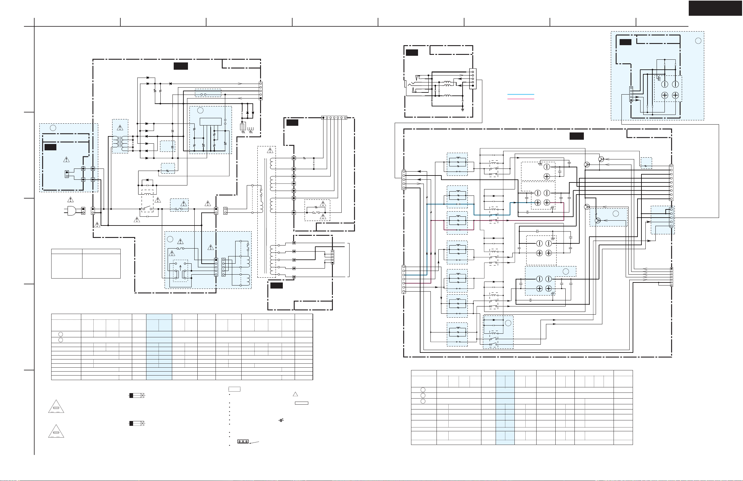
HT-R560
A
BCDEFGH
SCHEMATIC DIAGRAMS-5 (SD-5)
SPEAKER TERMINAL / POWER SUPPLY SECTION
1
LIST
U15
INLET PC BOARD
2
3
4
5
SUB TRANS.
LIST
E
NAETC-9437
P921B
INLET
P907
P901
TYPE
MDD, MDC
MPP, MPA, MPB
MGK, MGQ, MGR
MWT, MWO, MWF
MJJ
Refer to following table about the parts displayed by mark " LIST ".
TA5 : Jumper wire L=5 mm
MODEL No. --->
TYPE --->
D
E
NPT-
T901
NPT-
T902
C922
R921
R9101
F901
F902
F910
J931
CAUTION
FOR CONTINUED PROTECTION
AGAINST FIRE HAZARD, REPLACE
ONLY WITH FUSE OF SAME TYPE
VA
AND RATING INDICATED.
ATTENTION
AFIN D'ASSURER UNE PROTECTION
PERMANENTE CONTRE LES RISQUES
D'INCENDIE, REMPLACER UNIQUEMENT
VA
PAR UN FUSIBLE DE MEME TYPE
ET CALIBRATION COMME INDIQUE.
P921A
P922A
P922B
P901A
AC IN
120V, 60Hz
230V, 50Hz
220V, 50/60Hz
120V/220-240V, 50/60Hz
100V, 50/60Hz
TX-SR506 HT-R667 HT-R960 TX-SR606 TX-SA606X
MDD,
MPP,
MDC
MPB
1516D 1516P 1516P 1516DG
1520JQ 1520JQ1520GQ 1520GQ 1520GQ 1520JQ 1520GQ 1520JQ 1520GQ 1520JQ 1520JQ 1520GQ 1520JQ 1520JQ1520GQ 1520GQ 1520JQ
47(1/2W)
0.1(1/2W) 0.1(1/2W) 0.1(1/2W) 0.1(1/2W)0.1(1/2W)
8A/125V 4A/250V
Yes NoneYes
T902
1
9
2
8
3
7
456
MGK,
MWT,
MGQ,
MWO,
MGR
MWF
YesNone YesNoneNone None None None None
None NoneNone None None None Yes
2200/35 2200/352200/25 2200/25 2200/25 2200/252200/25 2200/252200/16 2200/162200/16 2200/16 2200/16 2200/162200/16
None
0.22(1/W) 0.22(1/W)0.22(1/W) 0.22(1/W) 0.22(1/W)
4A/250VNone
None
D933
D935
C933
4.7/50
D921 - 925,
D930, 931, 933, 935
: 1SS133
D930
D931
D923
D921
C921
223Z
D924
D922
D925
C902
104J
RL901
C901
103M/275VAC
VOLTAGE
SELECTOR
HT-R518 HT-R560
MPP
MDD,
MDC
1517D 1517P 1516D 1516P 1574D 1574D 1574P 1552D 1552P 1552G 1552DQ 1552J
1517P
4A/250V 8A/125V 4A/250V 8A/125V 4A/250V
None None
Yes YesYes Yes Yes
THIS SYMBOL LOCATED NEAR THE FUSE INDICATES
THAT THE FUSE USED IS SLOW OPERATING TYPE
FOR CONTINUED PROTECTION AGAINST FIRE
HAZARD,REPLACE WITH SAME TYPE FUSE. FOR FUSE
RATING REFER TO THE MARKING ADJACENT TO THE SYMBOL.
CE SYMBOLE INDIQUE QUE LE FUSIBLE UTLISE EST
E LENT.POUR UNE PROTECTION PERMANENTE,N'UTILISER
QUE DES FUSIBLES DE MEME TYPE. CE DARNIER EST
INDIQUE LA QU LE PRESENT SYMBOL EST APPOSE.
U12
POWER SUPPLY PC BOARD
D934
MTZJ5.6B
100K
R934
+
C930
100/50
LIST
+
C922
LIST
R921
0V
LIST
F901
LIST
D
F902
S902
220-240V
120V
TX-SR576
MPP
MDD,
MDC
47(1/2W)47(1/2W)47(1/2W) 47(1/2W)47(1/2W) 47(1/2W) 47(1/2W) 47(1/2W) None 47(1/2W)
None
+5.6V
LIST
MPP,
MPA
R930
R931
J931
TA5
LIST
D
Q930
SI-3010KF
Vin
GND
Vout
1Vc2
4
3
100K
R932
100K
C931
10/50
R933
P911
P912
1
2
3
4
5
MDD
8A/125V
None None
NAPS-9432
POFF
5
+12VD
4
MPUGND
+10VS
POWERD
D911
1SS133
C911 102J
TA5
ADJ
J932
5
E901
82K
C932
100/16
10K
PRI.
E902
1
3
VIDEO PCB
3
To NAVD-9467
2
SD-4 : C5
1
JL901A
D912
1SS133
MAIN TRANS.
LIST
T901
U13
TRANS. SEC.
TERMINAL
PC BOARD
S4
S3
S2
8
8.2(1/2W)
9
10
11
NC
12
13
14
R9102
LIST
VIDEO PCB
To NAVD-9467
SD-4 : C5
JL9101A
123
FLAC2
FLAC1
104J
C9101
R9101
F910
NAPS-9433
WT, WO, WF type
1
2
3
4
5
U02
P15
S1
P6903B
P16
P17
P6900B
P18
P19
P6904B
TRANS. SEC. TERMINAL
PC BOARD
NAPS-9420
MDD,
MPP,
MGK,
MDC
MPP
MDC
MPA,
MPB
None
None
8A/125V 4A/250V 10A/250V
None
None None
5A/125V 5A/125VNone None NoneNone None None
NOTE
THE COMPONENTS IDENTIFIED BY MARK ARE CRITICAL FOR SAFETY
REPLACE ONLY WITH PART NUMBER SPECIFIED.
VOLTAGE (MEASURED WITH VOLTMETER) IS DC VOLTAGE.(No INPUT SIGNAL).
ALL PNP TRANSISTORS ARE EQUIVALENT TO 2SA1015-GR UNLESS OTHERWISE NoTED.
ALL NPN TRANSISTORS ARE EQUIVALENT TO 2SC1815-GR UNLESS OTHERWISE NoTED.
ALL DIODES ARE EQUIVALENT TO 1SS133 UNLESS OTHERWISE NoTED.
ELECTROLYTIC CAPACITORS ( ) ARE IN uF/WV.
ALL CAPACITORS ARE IN pF/50WV UNLESS OTHERWISE NoTED.
EX) 030- 3pF 330- 33pF 331- 330pF 333- 0.033uF
ALL RESISTORS ARE IN OHMS 1/4WATTS UNLESS OTHERWISE NoTED.
THE THICK LINES ON PC BOARD ARE THE PRINTING SIDE OF THE PARTS.
EX) PRINTING SIDE
CIRCUIT IS SUBJECT TO CHANGE FOR IMPROVEMENT.
MWT,
MGQ,
MWO,
MGR
MWF
None
5A/250V 12A/250V
5A/250V
!
MJJ
None
2200/16
None
Yes
SEC3_1
5
4
3
2
1
JL6952A
4
567
SEC3_2
SEC2_1
YELLOW
BLACK
GREEN
NC
SEC2_2
AMPLIFIER PCB
SD-2 : A5
To NAAF-9419
U14
HEADPHONE JACK
PC BOARD
P7201
PHONES
JL6605B
1
HPL
2
LSPE
3
HPR
4
HPDET
5
JL6600B
1
SPSBL
2
SPSL
3
SPL
4
SPC
5
SPR
6
AMPLIFIER PCB
SPSR
SD-2 : E5
7
SPSBR
To NAAF-9419 (2/2)
Refer to following table about the parts displayed by mark " LIST ".
MODEL No. --->
TYPE --->
L6600 - 6604
L6605, 6606
R6600 - 6606,
R6610 - 6616
R6605, 6606,
R6615, 6616
R6690
J6600, 6604,
J6619, 6620,
J6625, 6626, 6851
JL6604B
NAETC-9435
5
0V
4
2
3
7
8
1
MPUGND
A
B
C
L7201
022M
L7202
022M
102J
102J
L7203
022M
223J
C7202
C7203
C7204
D6600, 6603, 6605, 6607 : KDS4148U
TA5 : Jumper wire L=5 mm
R6691
390(1/2W)
R6692
390(1/2W)
MDD,
MDC
None S-1.3C S1.3C S-1.3CNone
None S-1.3C None S-1.3CNone
None
None
TA5 YesNone Yes
5
4
HPDET
3
2
1
JL6605A
102J
C7201
E7201
L6602
LIST
R6602
LIST
R6612
LIST
TA5
J6851
LIST
L6600
LIST
R6600
LIST
LIST
R6610
TA5
J6600
LIST
L6601
LIST
R6601
LIST
R6611
LIST
TA5
J6604
LIST
L6603
LIST
R6603
LIST
R6613
LIST
TA5
J6619
LIST
L6604
LIST
R6604
LIST
R6614
LIST
J6620
TA5
LIST
L6605
LIST
R6605
LIST
R6615
LIST
J6626
TA5
LIST
L6606
LIST
R6606
LIST
R6616
LIST
TA5
J6625
LIST
TX-SR506
MPP,
MGK,
MPB
MGQ,
MGR
22
22
10(1/2W) 10(1/2W) 10(1/2W)10(1/2W)33(1/2W)33(1/2W)33(1/2W)33(1/2W)
None
Yes None
MWT,
MWO,
MWF
HT-R518
MPP
<Note>
1. NC = No mount of parts.
2. SD-x : XY is short for Schematic Diagrams-x and each
sockets location, X = A to H, Y = 1 to 5.
AUDIO ANALOG SIGNAL
FRONT L
FRONT R
C6602
103J
RL6602
D6600
C6600
103J
RL6600
D6603
C6603
103J
RL6603
D6605
C6605
103J
RL6605
D6607
C6607
103J
RL6607
HT-R560 TX-SR576
MDD,
MDC
None YesYes
Yes
None
None None None None None
Yes
P6601
CENTER
SPEAKER
FRONT
SPEAKERS
LR
103J
C6640
P6602
C6650
102J
C6653
102J
P6603
R
LRL
103J
C6643
SURROUND
SPEAKERS
SURROUND
BACK SPEAKERS
R
L
103J
C6645
P6604
C6655
102J
LIST
B
MPP
MDD,
MDC
None None None None S-1.3C S-1.3C None
None
None
2222 22
22None 22 None
None
HT-R667 HT-R960 TX-SR606 TX-SA606X
MDD
MPP,
MPA
Yes Yes Yes Yes
S-1.3C
S-1.3C
None None None S-1.3C S-1.3C None
22
None None None
22
None
Yes Yes None Yes None Yes
U09
ZONE 2 SPEAKER
TERMINAL PC BOARD
5
4
3
2
1
JL6604C
U37
NATRM-9468
SPEAKER TERMINAL PC BOARD
103J
C6642
103J
C6641
C6651
A
103J
C6646
MDC MPP
C6654
C6644
LIST
C6656
102J
C6652
102J
102J
103J
102J
MDD,
MDC
Q6601
Q6602
Q6601 - 6604 : KRC105S
Q6603
0
Q6604
RN1405
R6693
MPP,
MPA,
MPB
MWT,
MGK,
MWO,
MGQ,
MWF
MGR
YesNone YesNone NoneNone Yes None
YesNone NoneNone NoneNone None None No
22
22
SPRLF
SPRLCS
SPRLSB
SPRLZ2
+3V
+3V
+3V
LIST
B
0V
MJJ
None
NoneYes Yes Yes Yes
NATRM-9428
102J
C6657
P6607
(Banana type)
103J
103J
C6647
C6648
R6690
JL6603B
LIST
RLGND
SBRSPE
SRSPE
RSPE
CSPE
LSPE
SLSPE
SBLSPE
SBRSPE
SBLSPE
SPBROUT
SPBLOUT
JL6604B
LIST
SPRLF
SPRLCS
SPRLSB
SPRLZ2
HPDET
MPUGND
+24V
1
2
3
4
5
6
7
8
9
5
4
3
2
1
JL9102A
1
2
3
4
5
6
7
LIST
C
102J
C6658
ZONE 2
SPEAKERS
L
R
AMPLIFIER PCB
To NAAF-9419 (2/2)
SD-2 : D5
NC
VIDEO PCB
To NAVD-9467
SD-4 : C4
Page 11
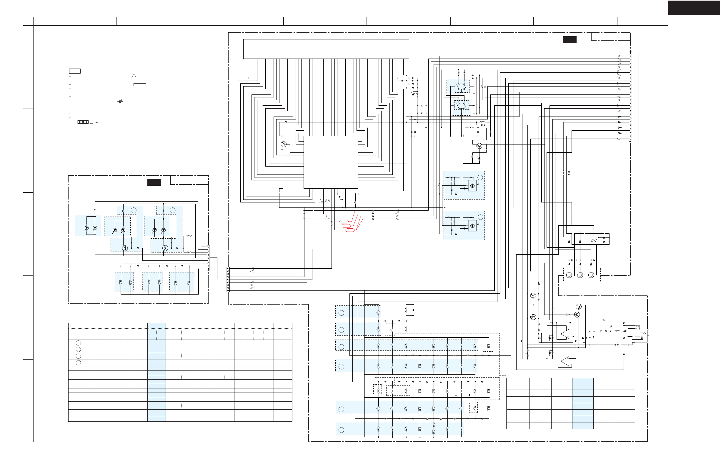
HT-R560
A
SCHEMATIC DIAGRAMS-6 (SD-6)
DISPLAY SECTION
1
2
3
4
5
NOTE
THE COMPONENTS IDENTIFIED BY MARK ARE CRITICAL FOR SAFETY
REPLACE ONLY WITH PART NUMBER SPECIFIED.
VOLTAGE (MEASURED WITH VOLTMETER) IS DC VOLTAGE.(NO INPUT SIGNAL).
ALL PNP TRANSISTORS ARE EQUIVALENT TO 2SA1015-GR UNLESS OTHERWISE NOTED.
ALL NPN TRANSISTORS ARE EQUIVALENT TO 2SC1815-GR UNLESS OTHERWISE NOTED.
ALL DIODES ARE EQUIVALENT TO 1SS133 UNLESS OTHERWISE NOTED.
ELECTROLYTIC CAPACITORS ( ) ARE IN uF/WV.
ALL CAPACITORS ARE IN pF/50WV UNLESS OTHERWISE NOTED.
EX) 030- 3pF 330- 33pF 331- 330pF 333- 0.033uF
ALL RESISTORS ARE IN OHMS 1/4WATTS UNLESS OTHERWISE NOTED.
THE THICK LINES ON PC BOARD ARE THE PRINTING SIDE OF THE PARTS.
EX) PRINTING SIDE
CIRCUIT IS SUBJECT TO CHANGE FOR IMPROVEMENT.
<Note>
1. NC = No mount of parts.
2. SD-x : XY is short for Schematic Diagrams-x and each sockets location, X = A to H, Y = 1 to 5.
3. Refer to SCHEMATIC DIAGRAMS-11 (SD-11) for FL driver IC control waveform.
2.2K
R7151
LIST
(RED)
D7152
SLI-343URC
LIST
D7151
STANDBY
SDPB3DD0C
(BLUE)
D7154
2SA1015
LIST
Q7151
!
LIST
82
C D
R7152
LIST
D7153
PURE AUDIO
10K
R7155
R7156
1K
R7103
560
LIST
LIST
S7108
S7107
ON/STANDBY
Refer to following table about the parts displayed by mark " LIST ".
MODEL No.--->
TYPE--->
MDD,
MDC
MPP,
MPB
MGK,
MGQ,
MGR
MWT,
MWO,
MWF
HT-R518
MPP
A
B
C
D
D7151
D7152
D7153
D7154
D7155
D7156
S7001, S7107
S7002, S7108
S7109
S7110
S7112, S7114 NoneYesNone
OPTIMIZER
None
None Yes
Yes
Yes Yes
None
MUSIC
Yes None
None NoneNone None
Yes
Yes YesYes
None NoneNone None
PURE
AUDIO
None NoneNone None
None NoneNone None
None None
Yes None
None
Yes
Yes
PURE
AUDIO
BCDEFGH
C7303
104J
471J
P7301
1
3
1K
R7407
D7401
TUNING
MODE
330
R7302
VIDEO
+
MTZJ5.1B
NADIS-9430
REMIN
FLDRST
FLDCS
FLDCLK
FLDSDO
KEY0
KEY1
KEY2
KEY3
+3.3VMPU
KEYINT0
FLAC1
KEYINT1
FLAC2
-VP
VOLA
VOLB
GNDDG
MICDET
+5VDIS
MICMUT
-15VA
MICOUT
+15VA
V3R
GNDV4_GNDMIC
V3L
GNDV4_GNDMIC
V3V
GNDV4V
LEDSTBY
C7304
104J
D7301
D7302
NC
R7303
MICDET
R7404
C7401
+
220
10/50
47K
R7405
TX-SR606 TX-SA606X
ZONE2
LEVEL UP
ZONE2
LEVEL DOWN
MEMORY
TUNING
MODE
C740347/25
E7301
C7402 101J
NC
NC
4.7K
R7403
L7401
022M
L7402
022M
NC
1
2
3
4
5
6
7
8
9
10
11
12
13
14
15
16
17
18
19
20
21
22
23
24
25
26
27
28
29
30
31
32
33
NC
R7401
47K
R7402
C7421
DIGITAL IN
DISPLAY
CINEMA
FILTER
None
LATE
NIGHT
33P
MICROPROCESSOR PCB
To NADG-9457
P701B
P7401
100
5
4
2
3
NC
7
8
NC
1
102J
SD-3 : A2
SETUP MIC
6G
3G
7G
4G
1G
F11
F12
1
2
5
6
7
8
9
11
10
12
LIST
S7110
R7154
LIST
D7155
120
R7104
820
ZONE 2
NADIS-9431
LIST
J7211
10K
R7157
R7158
NC
J7212
1K
R7105
1.2K
LIST
LIST
ZONE2
S7114
S7112
OFF (ZONE2)
9
8
7
6
5
4
3
2
1
JL7101B
9
8
7
6
5
4
3
2
1
JL7101A
LEDZONE2
LEDSTBY
GNDDG
+5VDIS
LEDPURE
KEY0_2
KEYINT0
GNDDG
C7001
U11
SWITCH PC BOARD
LIST
(GREEN)
D7156
SLR-342MGTE7P
Q7152
2SA1015
LIST
S7109
HT-R560 TX-SR576TX-SR506 HT-R667 HT-R960 TX-SR606 TX-SA606X
MDD,
MDC
MPP
MDD,
MDC
MPP,
MPA
MDD
MDC MPP
MDD,
MDC
MPP,
MPA,
MPB
MGK,
MGQ,
MGR
MWT,
MWO,
MWF
NoneYes YesYes Yes YesYes None
None
None
None
DOCK
None Yes
MUSIC
OPTIMIZER
Yes
Yes
None
None
Yes
YesNone YesNone
None
None
Yes Yes None
None
PURE
DOCK
AUDIO
None
None
Yes
None Yes
None
NoneNone
YesYesYes
NoneNoneNone NoneNone None
None
NoneNoneNone None NoneNone None
NoneNoneNone
THX
None
Yes
Yes Yes
None
None Yes
Yes
None
None
None
PURE
None
AUDIO
11G
10G
13
14
16
15
R7001 100K
Q7004
3
2SC2458-GR
1
2
+5V
223Z
MJJ
YesNone
Yes
None
NoneNone
None
Yes
None
YesYesNone
None
PURE
AUDIO
Q7001
16BT138GNK
FL TUBE
P6
P1
P7
P5
P3
P8
P4
14G
13G
16G
15G
12G
18
19
21
22
24
26
49
50
51
SEG0
52
VCC2
53
DIG15/SEG39
54
DIG14/SEG38
55
DIG13/SEG37
56
DIG12/SEG36
57
DIG11
58
DIG10
59
DIG9
60
DIG8
61
DIG7
62
DIG6
63
64
C7002 104J
C7003 101J
C7004 101J
C7005 101J
27
25
46
47
SEG5
SEG448SEG3
49 : SEG2
50 : SEG1
M66005-0001AHP
63 : DIG5
64 : DIG4
DIG032DIG023DIG014DIG005_RESET
1
17
20
P10
29
30
31P932
28
42
44
SEG943SEG8
SEG745SEG6
Q7003
FL DRIVER
_CS
SCK
6
7
8
P11
SDATA9P1
P12
J7011
P14
P13
34
33
39
SEG1240SEG1141SEG10
SEG19 : 32
SEG20 : 31
SEG32 : 18
SEG33 : 17
VCC1
10P011
18K
R7006
P15
P16
36
35
36
37
SEG15
SEG1438SEG13
XIN14VSS15SEG35
XOUT
12
13
101J
C7007
WF63
WF62
37
NC
WF61
38P239
34
P1823P17
SEG1735SEG16
P19
33
SEG18
SEG21
SEG22
SEG23
SEG24
SEG25
SEG26
SEG27
SEG28
SEG29
SEG30
SEG31
SEG34
16
C7008
P20
40
VP
100/10
P24
P22
P23
P21
41
42
44
43
32
31
30
29
28
27
26
25
24
-31.2V
23
22
21
20
19
18
17
P31
P32
P30
P28
P25
P29
P27
46
479G488G49
515G52
45
50
53
+5V
+
104J
C7009
R7002
R7003
R7004
R7005
3.3K
220
220
3.3K
FLDRST
FLDCS
FLDCLK
FLDSDO
LIST
A
KEY0
S7101
MULTI IN
R7101
330
LIST
B
LIST
A
KEY1
LIST
B
KEY2
S7102
MULTI IN
CD
S7115
CD
S7116
S7132
R7107
330
R7115
330
TUNER
TUNER
LIST
UP
KEY3
UP
TUNING
UP
TUNING
S7149
S7150
PRESET
R7123
330
PRESET
UP
A
LIST
B
P33
S7104
S7117
S7118
S7134
S7151
S7152
542G55
F22
F21
P35
P34
59
58
R7022
10K
S7002
LIST
R7046
1K
1K
2.2K
2.2K
+
C7045
+
C7041
S7127
VCR/DVR
S7128
VCR/DVR
(TONE)
S7161
SETUP
S7162
SETUP
R7023
10K
R7024
10K
L7031
022K
Q7033
2SC3198Y
C7033
100/6.3
U7042
REMOTE SENSOR
100/6.3
U7041
DVD
R7113
3.9K
DVD
R7121
3.9K
S7144
(TONE)
R7129
3.9K
L7032
+
S7129
S7130
S7146
S7164
3
10/50
C7022 103Z
C7031
LIST
LIST
J7050
1
B
A
R7114
12K
R7122
R7130
C7021
223Z
2
12K
12K
103Z
022K
+5V
D7033
MTZJ3.9B
S7106
S7148
TONE
S7166
DIMMER
C7032
82
R7033
223Z
R7412
FUNCTION
MODEL No.--->
S7104
S7106
S7132
S7134
S7136
S7164
Q7404
KRC111M
220
R7410
Q7403
KRC111M
+6.8V
220
R7409
+
10/16
C7405
33K
R7408
330J
470
C7404
R7413
220K
R7414
D7412
100K
-6.8V
D7411, 7412 :
MTZJ6.8B
TX-SR506
TX-SR576
OFF (ZONE2) SPEAKERS B
ZONE2
MEMORY MEMORY
DIGITAL INPUT NoneDIGITAL INPUTDIGITAL INPUT
DISPLAY DISPLAYDISPLAY DISPLAY
TUNING
MODE
C7010
R7102
470
R7108
470
R7116
470
R7124
470
223Z
NC
S7113
TAPE
S7119
S7120
TAPE
S7136
S7153
ENTER
S7154
ENTER
J7012
C7011
223Z
C7012 223Z
R7007
220
220
R7008
C7014
223Z
C7018
D7002
MTZJ8.2B
10/50
C7013
47/50
223Z
C7016
C7017
NC
R7013
R7109
560
AUX
S7122
R7117
560
S7138
GAME
S7155
DOWN
PRESET
R7125
560
S7156
DOWN
PRESET
C7015
NC
223Z
47/16
+
+
R7110
820
R7118
820
TUNING
R7126
820
AUX
GAME/TV
MUSIC
DOWN
DOWN
TUNING
S7123
S7124
S7140
S7157
S7158
R7111
1.2K
R7119
R7127
J7009
CBL/SAT
1.2K
RETURN
1.2K
RETURN
R7021
S7001
LIST
MASTER
VOLU ME
R7045
100
NC
C7046
102K
C7047
+3.3V
R7041
100
NC
C7042
102K
C7043
S7125
CBL/SAT
S7126
S7142
MOVIE/TV
S7159
S7160
10K
R7042
R7112
2.2K
R7120
R7128
U10
DISPLAY PC BOARD
J7053
J7054
104J
C7305
471J
C7301
C7302
330
R7301
L - AUDIO - R
AUX INPUT
Q7005
KRA102M
2 3
Q7007
470
KRC102M
7
Q7401:B
2
1
R7406
330
Q7401:A
4
5
6
8
3
2
Q7401 : NJM4580D-D
HT-R667
HT-R960
SPEAKERS A
MEMORY
DIGITAL INPUT
R7411
MICMUT
47/25
D7411
+
C7411
+
47/25
C7412
1
HT-R518 HT-R560
LATE
NIGHT
CINEMA
FILTER
TUNING
MODE
Page 12
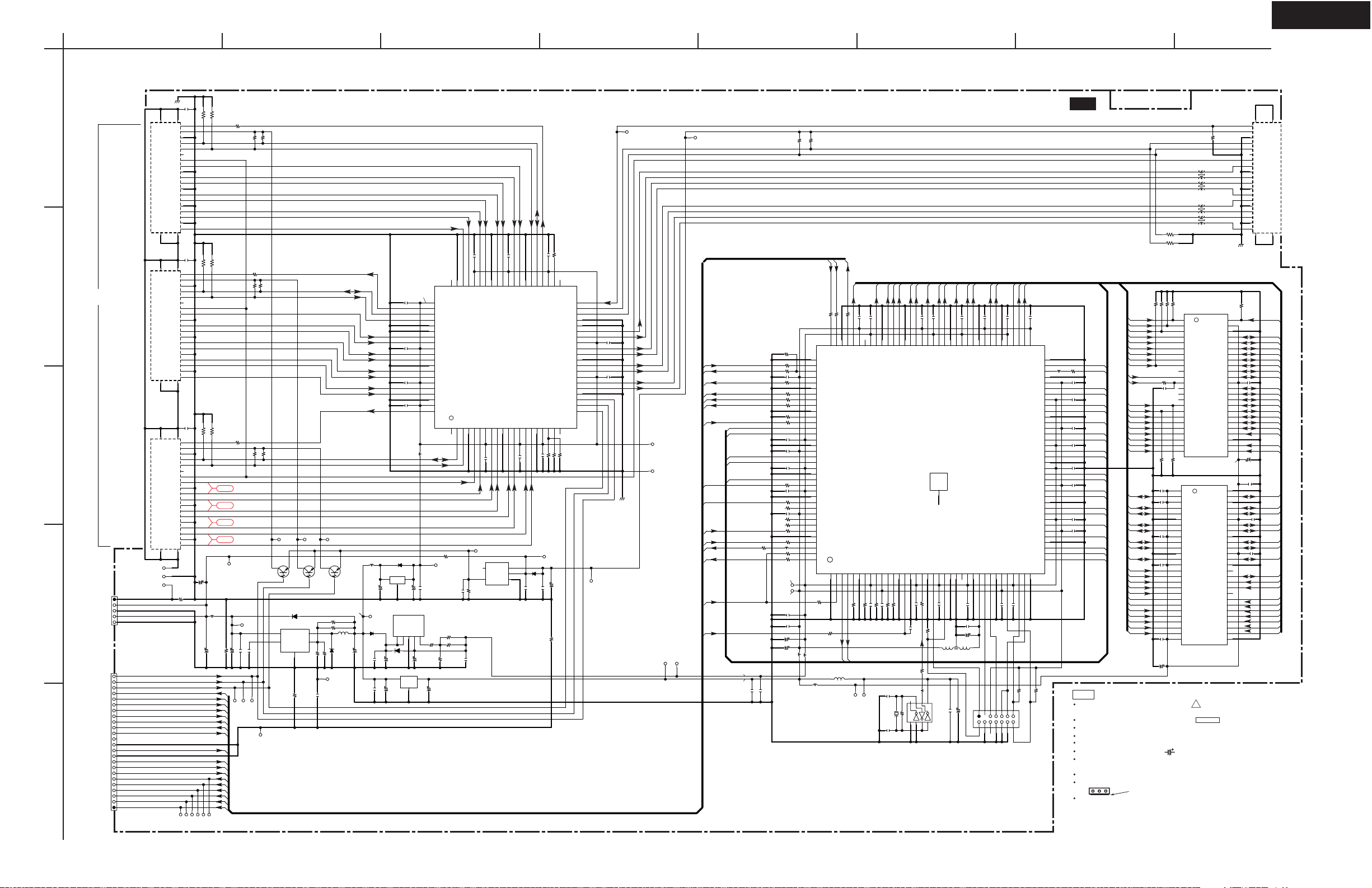
HT-R560
A
SCHEMATIC DIAGRAMS-7 (SD-7)
DSP / HDMI SECTION
AGND
22
1
IN 3
2
HDMI
IN 2
3
IN 1
JL801B
1
+12VHD
VIDEO PCB
SD-4 : H3
2
3
4
5
GNDP
+12VHD
GNDP
4
Shield
DDC DATA
DDC CLK
CERemote
CK Shield
P8001
D0 Shield
D1 Shield
D2 Shield
Shield
23
22
Shield
DDC DATA
DDC CLK
CERemote
CK Shield
P8002
D0 Shield
D1 Shield
D2 Shield
Shield
23
22
Shield
DDC DATA
DDC CLK
CERemote
CK Shield
P8003
D0 Shield
D1 Shield
D2 Shield
Shield
23
TP7
TP6
TP5
HP DET
HP DET
HP DET
To NAVD-9467
HDMSEL3
24
HDMSEL2
23
HDMSEL1
22
DIGSDO_DSP
21
DIGSDI
20
DSP_CLK
19
DSPRST
18
DSPCS
17
DSPINT2
16
DSPINT0
15
DSPINT1
14
13
12
DSP_RMCK
11
10
SD-3 : F4
SAI_SDOUT
5
9
SAI_LRCK
8
MICROPROCESSOR PCB
To NADG-9457
SAI_SCLK
7
CX_SDIN4
6
CX_SDIN3
5
CX_SDIN2
4
CX_SDIN1
3
CX_SCLK
2
CX_LRCK
1
P704B
SBL/SBR
SL/SR
FL/FR
CENTER / SUB
GND
GND
GND
CK+
NC
NC
C8019
103Z
20
19
18
+5V
17
16
15
14
NC
13
12
CK-
11
10
CK+
9
D0-
8
7
D0+
6
D1-
5
4
D1+
3
D2-
2
1
D2+
21
C8020
103Z
20
19
18
+5V
17
16
15
14
NC
13
12
CK-
11
10
CK+
9
D0-
8
7
D0+
6
D1-
5
4
D1+
3
D2-
2
1
D2+
21
C8021
103Z
20
19
18
+5V
17
16
15
14
NC
13
12
CK-
11
10
9
D0-
8
7
D0+
6
D1-
5
4
D1+
3
D2-
2
1
D2+
21
GND
R8021
0
TP36
TP38
TP37
R8006
R8005
NC
NC
R8012
R8011
+5VIN2HD
NC
NC
R8018
R8017
+5VIN3HD
WF42
WF41
WF41
WF41
+12V
C8198
220/25
L8015 : BLM21PG221
L8015
R280
C8199
220/25
TP41
TP39
TP40
R8001
1K
47K
R8002 47K
R8003
R8007
1K
47K
47K
R8009
R8008
R8013
1K
R8014
R8015
47K
47K
+5VIN1HD
TP9
+12V
TP10
220/25
223K
0
C8077
C8078 104K
C8076
TP4
TP3
TP02
TP01
BCDEFGH
GND_S
22
20
19
HP DET
18
+5V
Shield
17
GND
16
DDC DATA
15
DDC CLK
14
NC
13
CERemote
12
CK-
11
CK Shield
10
CK+
9
D0-
8
D0 Shield
7
D0+
6
D1-
5
D1 Shield
4
D1+
3
D2-
2
D2 Shield
1
D2+
21
AGND
10K
R281
48
47
46
45
44
43
42
41
40
39
38
37
36
35
34
33
32
31
30
29
28
27
26
25
C281
220/4
C295
104Z
54
53
52
51
50
49
48
47
46
45
44
43
42
41
40
39
38
37
36
35
34
33
32
31
30
29
28
C282
104Z
C291
104Z
C290
104Z
GPIO4GPIO3
D15
D7
D14
D6
D13
D5
D12
D4
D3
D10
D2
D9
D1
D8
D0
OE
FLCS
BA1
D15
D14
D13
D10
D9
UDQM
CLK
CKE
HDMI
P8004
OUT
Shield
23
D11
D12
D11
D8
A11
A9
A8
A7
A6
A5
A4
TP17
SI8008TM
1
VIN
5
SS
Q8004
D8002
1SS355
Q8006
GND
3
R8929
+5VIN2HD
TP18
DTC114TKA
2
SW
4
VADJ
100
+5VIN3HD
Q8005
DTC114TKA
R8931 33K
R8934 3.3K
1.5K
R8932
R8933 1.5K
104K
C8079
TP8
TP19
L8014
470K
D8001
CRS09
Q8009
DTC114TKA
+4.1V
C8075
BLM21PG221
L8007
C8016
TP11
+3.5V
D8003
1SR154
-400
470/10
104Z
C8074
C8068
BA33BC0FP
100/16
C8073
104Z
C8067
C8009 103K
C8010 103K
C8011 103K
C8012 103K
D8007
Q8002
1
I
G
2
BD7820
_SHUT
1
1SS355
D8004
10/16
Q8008
1
10/16
3
O
Q8007
INPUT
GND4OUTPUT
2
3
TA48033AF
I
G
2
+3.3V
L8008
LBC2518
220/4
C8015
5
O
+3.3V
DAJ
C8072
3
61
62
63
64
65
66
67
68
69
70
71
72
73
74
75
76
77
78
79
80
104Z
C8014
R8936
100/4
C8066
0
Vcc
HPD2
SDA2
SCL2
GND
GND
B21
A21
Vcc
B22
A22
GND
B23
A23
Vcc
B24
A24
GND
Vcc
HPD1
R8935
+3.3V
100/4
R8028
TP22
59
60
NC
1NC2
+5VIN_DET
47
C8022
R8937
39K
R8938
39K
33K
GND
SDA1
104Z
58
3
57
A34
SCL1
4
+1.2V
C8071
C8008 103K
B34
GND
104Z
55
56
53
54
Vcc
B33
A33
GND
TMDS341A
HDMI SWITCH
B11
Vcc
A11
B12
5
6
8
7
103K
C8001
TP12
5
NC
S-812C50BUC
10K
Q8003
R8020
51
52
A32
Q8001
A12
9
10
OUT
IN
GND4SW
B32
GND
U42
HPD_SINK
TP20
1K
C8007 103K
48
49
50
Vcc
A31
A1313Vcc
B13
11
12
103K
C8002
1
2
3
R8019
C8006 103K
+3.3V
46
41NC42OE43
44
45
47
Vcc
B31
GND
SCL3
SDA3
HPD3
40
HPD_SINK
39
SDA_SINK
38
SCL_SINK
37
GND
36
GND
35
Z1
34
Y1
C8005103K
33
Vcc
32
Z2
31
Y2
30
GND
29
Z3
28
Y3
C8004 103K
27
Vcc
26
Z4
25
Y4
24
GND
23
S3
22
S2
21
S1
A14
Vcc
B14
PRE20NC
VSADJ
GND
14
15
16
17
19
18
27K
10K
5.6K
R8010
R8016
C8003 103K
R8004
AGND
+12V
TP13
D8006
C8013
104Z
C8017
104Z
R8027
C8018
0
33/10
+5.0V
TP14
TP16
TP15
TP30
TP31
+5VOUT+5VIN1HD
TP21
DIGSDO_DSP
DIGSDI
CX_SDIN1
CX_SDIN2
CX_SDIN3
CX_SDIN4
SAI_SDOUT
GPIO1
GPIO2
GPIO3
GPIO4
GPIO5
DSPINT1
DSPINT0
SAI_SCLK
SAI_LRCK
CX_SCLK
CX_LRCK
DSP_RMCK
DSPRST
+1.2V
+3.3V
GNDDG
R267
47
C245104Z
R273
R252
R253
C231
R254
R255
R256
R257
R258
R259
C214 104Z
C232 104Z
C215 104Z
R260
C216
R261
R262
C233 104Z
R263
R264
R265
R266
L312
R268
R269
C218
C235
C246104Z
+1.2V
TP33
TP32
+3.3V
C217
1.8K
1.8K
R8023
R8024
DSP_CLK
220
R251
+3.3V
+1.2V
109
110
111
112
113
114
115
AXR0[1]
116
AXR0[2]
117
AXR0[3]
118
VSS
119
AXR0[4]
120
AXR0[5]/SPI1_SCS
121
AXR0[6]/SPI1_ENA]
122
AXR0[7]/SPI1_CLK
123
CVDD
124
VSS
125
DVDD
126
AXR0[8]/AXR1[5]/SPI1_SOMI
127
AXR0[9]/AXR1[4]/SPI1_SIMO
128
CVDD
129
VSS
130
AXR0[10]/AXR1[3]
131
AXR0[11]/AXR1[2]
132
CVDD
133
VSS
134
AXR0[12]/AXR1[1]
135
AXR0[13]/AXR1[0]
136
DVDD
137
AXR0[14]/AXR2[1]
138
AXR0[15]/AXR2[0]
139
ACLKR0
140
VSS
141
142
143
144
R200
330
R206
220
L201
L202
LBC2518T470M
L282
108
SPIO_CLK/I2C0_SCL
VSS
1
10K
330
47
104Z
47
47
47
47
10K
330
47
104Z
47
330
330
330
330
330
LM182
330
47
104Z
C234
104Z
220/4
220/4
L201, 202 : BLM21PG221SN1
DSPCS
DSPINT2
OE
220
47
104Z
C230
R209
R250
102
103
104
105
106
107
VSS
DVDD
EM_OE
EM_RW
109 : VSS
110 : SPIO_SIMO
111 : SPIO_SOMI/I2C0_SDA
SPIO_SCS/I2C1_SCL
SPIO_ENA/I2C1_SDA
112 : DVDD
113 : AXR0[0]
114 : VSS
141 : AFSR0
142 : ACLKX0
143 : AHCLKR0/AHCLKR1
144 : AFSX0
AHCLKX0/AHCLKX2
AMUTE0
AHCLKX1
AMUTE1
VSS7ACLKX18CVDD
3
5
6
2
4
10K
10K
R202
R201
GPIO6
GPIO7
L205
+3.3V
TP34
TP35
C213
101
C201 104Z
FLCS
104Z
100
CVDD
9
10K
R203
RAS
98
99
VSS
EM_CS[2]
ACLKR1
DVDD11AFSX1
10
10K
C221 104Z
R204
C238
060D
X202
C239
060D
BA0
SDCS
96
97
EM_RAS
EM_BA[0]
EM_CS[0]
AFSR1
12
13
10K
R205
17.734MHz
A0
A10
BA1
C229
C212
104Z
104Z
90
91
92
95
94
VSS
D788E001BRFP266
VSS
RESET15VSS16CVDD17CLKIN
14
L204
LM182
1M
4
R272
93
EM_A[10]
EM_BA[1]
104Z
C202
C243 101J
0
R270
GND
3
DVDD
Q201
18
R207 220
R208
CLKIN2
TRST
765
2
1 8
89
CVDD
EM_A[0]
EM_A[1]
DSP
THERMALPAD
145
GNDDG
VSS19TMS
CVDD21TRST22OSCVSS23OSCIN
20
C203 104Z
10K
ACF451832-333
TMS
VD
Q202
TC7WU04FU
88
EM_A[2]
A3A2A1
C211
85
86
87
VSS
CVDD
EM_A[3]
OSCOUT25OSCVDD26VSS
24
C242
104Z
C241
220/4
L241
104Z
C236
C237 100/4
INVERTER
A6
A5
A4
A7
C228
104Z
104Z
80
81
79
82
83
84
VSS
DVDD
EM_A[7]
EM_A[4]
EM_A[6]
EM_A[5]
VSS : 72
EM_CKE : 71
EM_CLK : 70
EM_WE_DQM[0] : 39
EM_WE : 38
EM_CAS : 37
TDO30VSS31DVDD
PLLHV28TDI
27
29
C204 104Z
TDI
TDO
3
7
5
1
P202
2
8
4
6
C219
104Z
77
78
VSS
CVDD
EM_WE_DQM[1]
EMU[0]
CVDD
32
33
104Z
C205
C222 104Z
EMU0
9
11
101214 13
75
EM_A[9]76EM_A[8]
EMU[1]
34
EMU1
A11A9A8
C227
104Z
74
73
DVDD
EM_A[11]
VSS
DVDD
EM_D[8]
CVDD
EM_D[9]
EM_D[10]
VSS
EM_D[11]
DVDD
EM_D[12]
EM_D[13]
CVDD
EM_D[14]
EM_D[15]
VSS
CVDD
EM_D[0]
EM_D[1]
DVDD
EM_D[2]
EM_D[3]
VSS
EM_D[4]
EM_D[5]
CVDD
EM_D[6]
DVDD
EM_D[7]
VSS
TCK36VSS
35
TCK
4.7K
R289
JTAG
DSP / HDMI PC BOARD
72
71
R221
L203
70
LL121
75
69
C226
68
67
104Z
66
C209
65
64
104Z
63
62
61
C225
60
59
104Z
58
C208
57
56
104Z
55
54
C207
53
52
104Z
51
C224
50
49
104Z
48
47
46
45
C206
44
43
104Z
C223
42
41
104Z
40
39
38
37
+1.2V
+3.3V
4.7K
R290
NOTE
THE COMPONENTS IDENTIFIED BY MARK ARE CRITICAL FOR SAFETY
REPLACE ONLY WITH PART NUMBER SPECIFIED.
VOLTAGE (MEASURED WITH VOLTMETER) IS DC VOLTAGE.(NO INPUT SIGNAL).
ALL PNP TRANSISTORS ARE EQUIVALENT TO 2SA1015-GR UNLESS OTHERWISE NOTED.
ALL NPN TRANSISTORS ARE EQUIVALENT TO 2SC1815-GR UNLESS OTHERWISE NOTED.
ALL DIODES ARE EQUIVALENT TO 1SS133 UNLESS OTHERWISE NOTED.
ELECTROLYTIC CAPACITORS ( ) ARE IN uF/WV.
ALL CAPACITORS ARE IN pF/50WV UNLESS OTHERWISE NOTED.
EX) 030- 3pF 330- 33pF 331- 330pF 333- 0.033uF
ALL RESISTORS ARE IN OHMS 1/4WATTS UNLESS OTHERWISE NOTED.
THE THICK LINES ON PC BOARD ARE THE PRINTING SIDE OF THE PARTS.
EX) PRINTING SIDE
CIRCUIT IS SUBJECT TO CHANGE FOR IMPROVEMENT.
<Note>
1. NC = No mount of parts.
2. SD-x : XY is short for Schematic Diagrams-x and each sockets location, X = A to H, Y = 1 to 5.
3. Refer to SCHEMATIC DIAGRAMS-10 (SD-10) for HDMI signal waveform.
NAHDM-9475
CKE
CLK
UDQM
D8
D9
D10
D11
D12
D13
D14
D15
D0
D1
D2
D3
D4
D5
D6
D7
LDQM
WE
CAS
R8026
R8025
L8001 - 8004 : MNR12E0APJ000
R284 10K
R283 10K
R282 10K
R285 10K
GPIO2
GPIO1
A11
A10
A9
A8
A7
GPIO7
WE
R286
DSPRST
330
C283 102J
GPIO6
GPIO5
A6
A5
A4
A3
A2
A1
A0
10K
R288
R287
C285
104Z
D0
C286
104Z
D1
D2
D3
D4
C287
D5
104Z
D6
D7
C288
104Z
LDQM
WE
CAS
RAS
SDCS
BA0
BA1
A10
A0
A1
A2
A3
C289
104Z
C284
+3.3V
220/4
L8001
L8002
L8003
L8004
NC
NC
1
2
3
4
5
6
7
8
9
10
11
12
13
14
15
16
17
18
19
20
21
22
23
24
10K
1
VDD
2
DQ0
3
VDDQ
4
DQ1
5
DQ2
6
VSSQ
7
DQ3
8
DQ4
9
VDDQ
10
DQ5
11
DQ6
12
VSSQ
13
DQ7
14
VDD
15
LDQM
16
WE
17
CAS
18
RAS
19
CS
20
BA0
21
BA1
22
A10
23
A0
24
A1
25
A2
26
A3
27
VDD
A15
A14
A13
A12
A11
A10
A9
A8
A19
A20
WE
RESET
NC
WP/ACC
RY/BY
A18
A17
A7
A6
A5
A4
A3
A2
A1
R8022
47K
2 3
1
2
1 4
2
1 4
2
1 4
Q281
!
4
3
3
3
A16
BYTE
GND
Q15/A-1
Q7
Q14
Q6
Q13
DSP ROM
Q5
Q12
FLASH MEMORY
Q4
VCC
Q11
Q3
Q10
Q2
Q9
Q1
Q8
Q0
ES29LV160ET-70TG
or S29AL016D70TFI010
OE
GND
CE
Q282
A0
+3.3V
VSS
DQ15
VSSQ
DQ14
DQ13
VDDQ
DQ12
DQ11
VSSQ
DQ10
SDRAM
DQ9
VDDQ
DQ8
VSS
NC
UDQM
CLK
CKE
NC
A11
A9
A8
M12L64164A-7TG
K4S641632K-UC60
A7
A6
A5
A4
VSS
Page 13
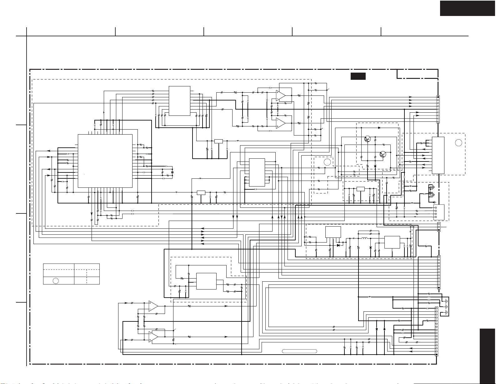
HT-R560
A
SCHEMATIC DIAGRAMS-8
SIRIUS / DOCK TERMINAL SECTION
1
NC
L2002
C2013
R2057
44
42
43
46
48
45
47
VDD
SAII_EN
SAII_DA
12 : SLAVE_SEL
I2S_RATE
LINKACTIVE15COMM_TX_EN
16
13
14
R2005
R2006
R2007
R2038
MPP
MUTE
SAII_CLK
Q2001
VDD
VSS
17
18
C2003
C2004
I2S_OCLK
COMM_RX_P
19
1
LSDP
2
VSS
3
R2004
SC_TX_OUT
4
VDD
5
SC_RX_IN
6
I2C_SCL
7
I2C_SDA
8
VDD
9
ANT_REV
10
VSS
11
RST
12
HT-R560
MDD,
MDC
Yes None
C2001
R2043
R2002
2
C2002
R2001
XM_SDI_L
R2003
XM_SDO_L
XM_RESET
XM_IRQ_ANT
3
Refer to following table about the parts displayed by mark " LIST ".
MODEL No.--->
TYPE--->
A
4
C2012
41
38
39
40
VSS
VDD
I2S_CLK
I2S_LRCLK
DT4_MODE
HSDP_CLK
VSS
VDD
COMM_RX_M
COMM_TX_M
20
22
21
23
R2008
R2009
I2S_OCLK
I2S_SCLK
I2S_SDO
I2S_LRCLK
XMDACRST
37
VSS
I2S_DA
HSDP_EN
VDD
HSDP_DA
VSS
TEST
SC_RATE
OSC_IN
VDD
OSC_OUT
VSS
COMM_TX_P24VSS
C2005
C2006
Q2004 : NJM4580M-D
R2108
33K
R2109
33K
36
35
34
33
32
31
30
29
28
27
26
25
C2007
33K
R2105
33K
R2104
R2045
R2044
C2010
BCDE
<Note>
1. NC = No mount of parts.
2. SD-x : XY is short for Schematic Diagrams-x and each sockets location, X = A to H, Y = 1 to 5.
RXDXMSRRXD-
TXD
2
4
1SS352
1K
R2073
SW
VADJ
NC
R2072
Q2008
GND
R2089
D2083
470
3
NADG-9458
IPOD_AUDIO_L
IPOD_AUDIO_R
R2074
0
102K
C2044
L2006
R2076
L2004
R2033
C2034
C2042
R2034
L2005
IPOD_VIDEO_OUT
L2082
1
VIN
5
SS
C2086
C2087
C2088
R2090
NC
0
R2080
NC
C2084
104Z
NC
R2083
R2082
R2081
NC
NC
GND_Floating_A
XM_L_OUT
XM_R_OUT
GND_A
SR_L_OUT
SR_R_OUT
11
R2040
10
0
C2040
P2001
+12V_XM
GND_XM
R2075
NC
XMSRSEL
XMDACRST
XMRST
XM_IRQ_ANT
XM_LNK
XMSRRXD
XMSRTXD
DCKDET
DCKRXD
DCKTXD
R2093
C2097
C2085
R2092
C2083
RX
104Z
TX
DCKDET
R2091
330K
GND_D
+12V
+12V
IDENTIFY
IPOD_Video
AUDIO_R
AUDIO_L
P2080
P2002
9
8
7
6
5
4
3
2
1
104Z
104Z
GND
SHIELD
SHIELD
L_OUT
AGND
TX
R_OUT
GND
RX
RESET
VIN
4
3
2
1
NC
0
16
15
14
13
12
11
10
9
8
7
6
5
4
3
2
1
1
2
3
4
5
6
7
8
9
E2003E2001
GND
D+
D-
+V
3
2
1
11
10
9
8
7
6
5
4
3
2
1
JL5502B
AMPLIFIER PCB
SD-1 : B1
To NAAF-9419
LIST
A
SIRIUS
NC
VIDEO PCB
SD-4 : G3
JL8002B
To NAVD-9467
SD-3 : E1
JL101B
MICROPROCESSOR PCB
To NADG-9457
SHIELD_GND
DOCK
R2012
R2013
R2014
R2015
R2066
R2046
C2011
R2037
R2106
R2107
3
2
33K
33K
6
5
C2060
R2060
R2011
+3.3V_XM
Q2004:B
R2110
33K
R2111
33K
8
Q2004:A
4
R2061
C2008
1
7
R2062
C2009
R2010
Q2002
1
MLCK
2
BICK
3
SDTI
4
LRCK
5
RSTN
6
SMUTE
7
ACKS
8
DIF09DIF1
X2001
L2001
NC
C2102
R2115
C2100
+14.8V
C2079
10/50
-14.8V
DZF
DEM
VDD
VSS
VCOM
AOUTL
AOUTR
C2101
R2119
C2077
10/50
C2078
10/50
16
15
14
13
12
11
10
C2033
1
2
3
R2063
3
L2007
Q2007
O
Vout
GND
V+
R2064
2
R2065
G
C2061
3O1
C2033
C2032
1
I
C2032
XM_RESET
XM_SDI_L
XM_IRQ_ANT
XM_SDO_L
XM_LNK
XMDACRST
Q2072
VGND
Vin
IPOD_AUDIO_L
IPOD_AUDIO_R
Q2005
C2043
R2020
R2019
G
2
5
4
I
R2047
C2104
C2031
C2103
C2021
C2022
L2003
R2116
R2117
R2023
R2024
C2035
C2036
1
2
3
4
5
6
7
8
R2118
R2021
R2022
Q2006
1Y
0Y
YCOM
1Z
XCOM
ZCOM
0Z
INH
VEE
GND9C
C2039
R2025
R2026
VCC
R2031
C2027
C2029C2030
NC
R2126
R2127
NC
R2048
22
R2049
22
R2032
NC
LIST
R2054
R2055
R2056
Q2009
R2125
-15V
+15V
A
0
0
0
OUTPUT
DAJ
5
3
4
C2092
R2079
R2078
C2025
4
Q2003:A
5
7
6
8
R2027
C2037
R2029R2030
C2038
R2028
2
C2024 C2023
3
C2026
16
15
14
13
1X
12
0X
11
A
10
B
1
Q2003:B
DCKRXD
DCKTXD
DCKDET
IPOD_Video
IPOD_L
IPOD_R
L/R_TO_Floating_IN
C2028
U31
SIRIUS / DOCK TERMINAL
PC BOARD
+15V
-15V
[+5V Level Shift]
D2088
+5V
XMRST-
R2070
R2071
NC
C2048
220K
C2047
L2083
C2081
C2090
102J
Q2012
R2052
C2049
0
0
Q2011
OGI
R2120
R2121
L2081
C2089
L2086
BLM21PG221SN1
R2085
R2086
102J
220K
R2087
C2082
C2046
D2086
0
0
R2050
R2053
D2087
C2045
R2122
Q2013
R2123
1SS352
R2051
D2082
GND
D2085
INPUT
2
0
0
XMSRTXD-
_SHUT
1
R2088
C2091
HT-R560
Page 14
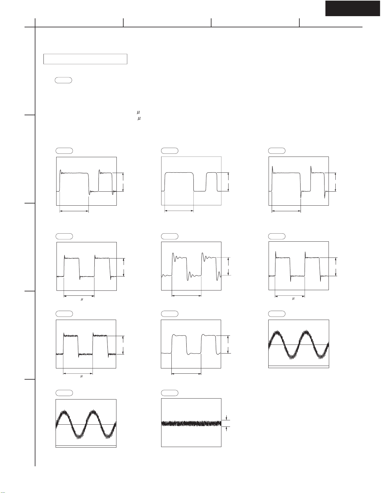
HT-R560
A
SCHEMATIC DIAGRAMS-9
WAVEFORM SECTION-1/3
Digital Audio Waveform Part
1
2
<Notes>
1. WF01 is short for Waveform-01 .
2. Refer to SD-3 (SCHEMATIC DIAGRAMS-3) for the location of each waveform on circuit.
3. SD-x : XY is short for Schematic Diagrams-x and each socket's location, X=A to H, Y=1 to 5.
LR CLOCK (SAI_LRCK, CX_LRCK)
Fs = 48kHz : DVD, Clock width = 20.8 s
Fs = 44.1kHz : CD, Clock width = 22.7 s
BIT CLOCK (SAI_SLCK, CX_SLCK)
64Fs = 3072kHz : DVD, Clock width = 325ns
64Fs = 2822.4kHz : CD, Clock width = 354ns
OPT1
WF01
(SD-3 : D5)
4.0V
BCD
WF02
COAX1
(SD-3 : D5) (SD-3 : E4)
5.0V
WF03
SAI_SDOUT
3.3V
Duty varies according to audio data
SAI_LRCK SAI_SLCK CX_SDIN1
WF04
(SD-3 : E4) (SD-3 : E4) (SD-3 : E4)
Duty always varies according to
audio data
WF05 WF06
Duty varies according to audio data
3
3.3V
20.8
s
CX_LRCK CX_SCLK DAC_OUT-
WF07
(SD-3 : E4) (SD-3 : E4) (SD-3 : C5)
WF08 WF09
325 ns
3.3V
20.8 s
3.3V
4
3.3V
20.8
s
AUDIO_FL WF10
WF10
(SD-3 : B5) (SD-3 : B5)
325 ns
AUDIO_FL
3.3V
Analog audio waveform with
aliasing noise
2.8V
0V
5
Analog audio waveform with
aliasing noise
2.8V
0V
Aliasing noise in no audio data
220mVp-p
Page 15
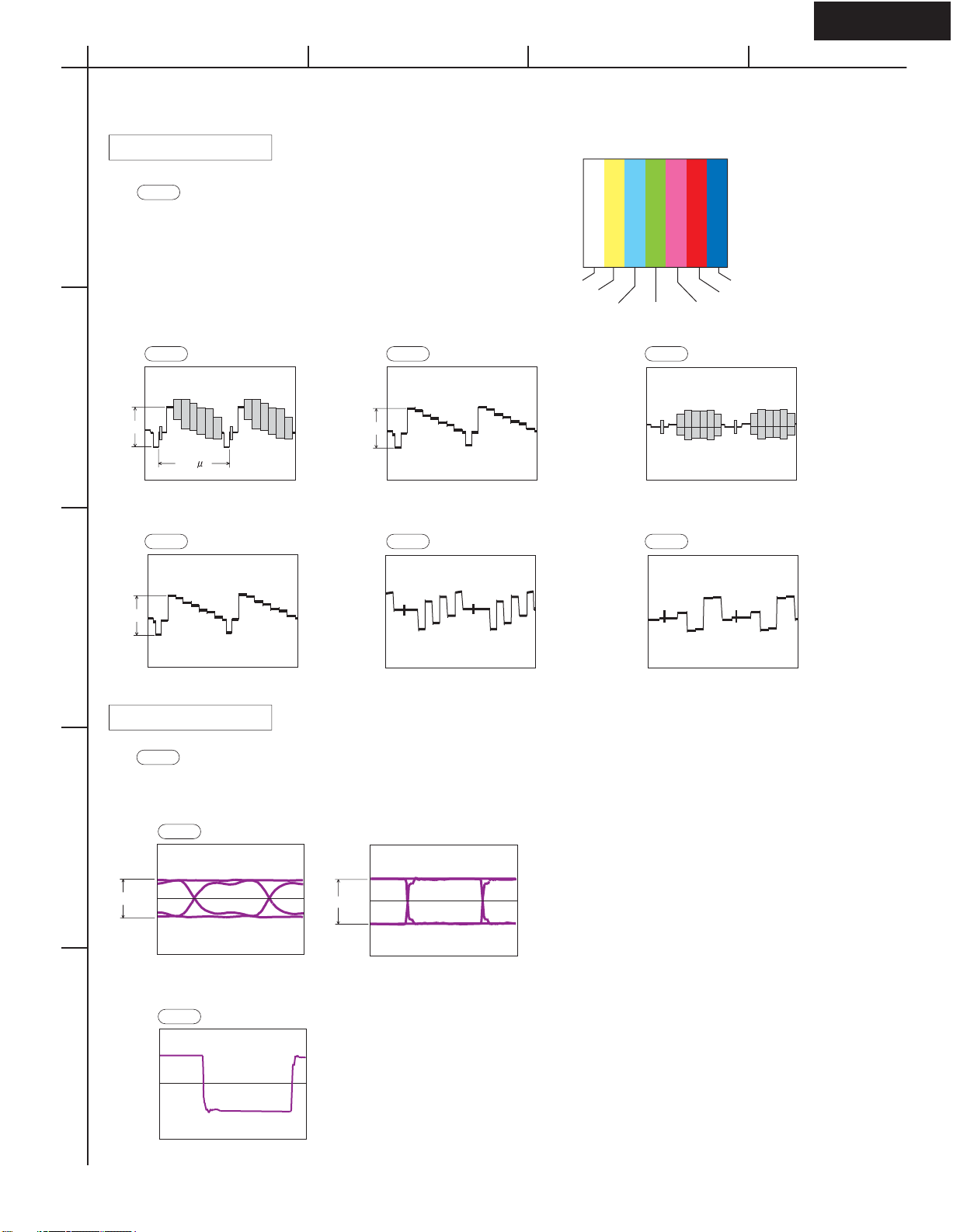
HT-R560
A
SCHEMATIC DIAGRAMS-10
WAVEFORM SECTION-2/3
Video Waveform Part
1
2
<Notes>
1. WF21 is short for Waveform-21 .
2. Refer to SD-4 (SCHEMATIC DIAGRAMS-4) for the location
of each waveform on circuit.
3. SD-x : XY is short for Schematic Diagrams-x and each
socket's location, X=A to H, Y=1 to 5.
4. In the case that video outputs are not connected to video devices,
video signal output levels are doubled.
Composite waveform S-Video Y waveform
(SD-4 : B4)
WF21
1V
6.36 s
(NTSC)
1.2 Vp-p (H)
BCD
Video source color and pattern
White
Yellow
WF22
(SD-4 : B4) (SD-4 : B4)
1V
1.0 Vp-p
Green
Cyan
S-Video C waveform
WF23
Magenta
Blue
Red
280 mVp-p
Component Y waveform Component PB waveform Component PR waveform
WF24
3
1V
HDMI Waveform Par t
<Notes>
1. WF41 is short for Waveform-41 .
2. Refer to SD-7 (SCHEMATIC DIAGRAMS-7) for the location of each waveform on circuit.
3. SD-x : XY is short for Schematic Diagrams-x and each socket's location, X=A to H, Y=1 to 5.
4
360mV
(SD-4 : B2) (SD-4 : B2) (SD-4 : B2)
1.0 Vp-p
HDMI D0,D1,D2 waveform
WF41
SD-7 : B3
2,227.5MHz
(1080p,12bit)
600mV
WF25 WF21
720 mVp-p 728 mVp-p
D0,D1,D2 Eye-pattern waveform, frequency and level vary
according to video resolution, aspect and profile.
Waveforms above are examples.
27MHz
(480i, 8bit)
HDMI CK waveform
WF42
5
SD-7 : B3
222,75MHz
(1080p,12bit)
CK waveform, frequency and level differ according to video resolution, aspect and profile.
D0,D1,D2 are just CK x10.
Page 16
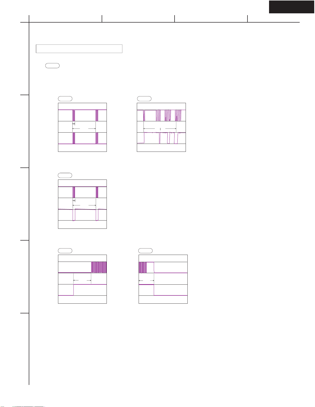
HT-R560
A
SCHEMATIC DIAGRAMS-11
WAVEFORM SECTION-3/3
FL Driver IC Control Waveform Part
1
2
<Notes>
1. WF61 is short for Waveform-61 .
2. Refer to SD-6 (SCHEMATIC DIAGRAMS-6) for the location of each waveform on circuit.
3. SD-x : XY is short for Schematic Diagrams-x and each socket's location, X=A to H, Y=1 to 5.
SCK/SDATA waveform
WF61 WF61
SD-6 : D3
5V
SCK
0V
2ms
5V
12ms
S DATA
0V
SCK
S DATA
BCD
SCK/SDATA waveform
SD-6 : D3
5V
0V
u
5V
0V
SDATA waveform varies according to
the data content
10 s
SCK/CS waveform
WF62
SD-6 : D3
5V
SCK
0V
3
2ms
12ms
5V
CS
0V
SCK/RESET waveform
SD-6 : D3WF63
5V
SCK
RESET
0V
0.45s
5V
RESET
0V
When power on
4
SCK/RESET waveform
SD-6 : D3WF63
5V
SCK
0V
0.6s
5V
0V
When power off
5
Page 17
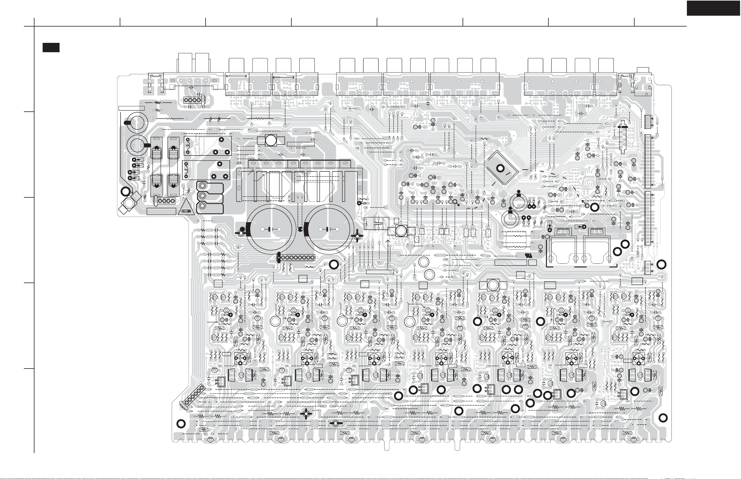
TX-SR506
A
PRINTED CIRCUIT BOARD VIEWS-1
U01
1
2
3
4
5
AMPLIFIER PC BOARD (NAAF-9419)
Component side
P6991
R5670
SPK HOLDER
C9003 C9004
F6901A
D9001
D9003
D9002
D9004
R5660
F6901
C9001
F6901B
R5661
10A 125V
BCDEFGH
1P
C6087
C6086
P6602
JL6604A
R5686 P7900
F6902A
C6076 C6077
R5673
J5044
J5043
F6902C
F6902D
R6197
F6902B
J5064
7
JL6600A
J5244
2SA/MP
ECB
Q6060
R5688
R5672
F6901C F6901D
F6902
JL6952B
R5687
30
RL6902
RL6901
P6904B
GRN
P6903B
YEW
P6900B
BLK
J5080
10
R6135
C6035
C6033
R6133
R6131
C6031
C6030
C6032
C6034
C6036
R5050
R5230
R5030
Q5050
D5000
R5170
C5020
R5100
Q5040
R5060
R5070
R5080
R6170
R6180
R6160
Q6070
C6050
25
25
7
J5215
27
27
R6100
27
7
R6090
15
J5245
P7908
R5685
30
R6130
R6132
R6134
R6136
Q5000
R5020
C
Q5010
R6050
BIAS
J5159
10
P6080
ID+
ID-
J5206
J5212
12
J5214
J5217
J5213
J5210
17
J5240
J5241
10
ECB
Q6000
Q6050
J5011
12
J5042
RL6902
C6912
RL6901
D6901A
C6902
C6902
P6902A
C5040
R5090
C5100
C5090
R5190
R6040
Q6010
Q6040 Q6041 Q6042
J5158
7
J5208
25
2SC/MN
R5671
20
J5040
10
J5038
15
J5037
15
J5041
J5063
J5059
J5060
J5078
J5079
15
J5118
7
J5117
R5110
C5110
R5130 R5131
30
J5209
20
20
D6901
15
15
-+
30
30
J5141
C5010
R5010
7
27
7
J5140
12
J5139
R5000
Q5051
J5142
C5080
R5200
Q6030 Q6031 Q6032
D5001
C5000 C5001
C5021
R5101
Q5030
P6101
R5160
R5180
R6030
C5050
R6000
R6020
R6010
7
J5148
R6080
R6070
C6040
J5205
27
17
J5211
J5204
30
7
J5207
7
J5239
J5238
EC
Q6061
20
J5039
J5010
12
J5036
C6913
AC
dipping
after
Remove
30
30
R5041
R5040
10
J5116
Q5011
R5051
R5031
R5231
R5171
Q5041
R5061
R6181
R6161
Q6071
P6081
C6051
ID+
ID-
J5157
27
27
R6101
J5200
25
25
10
R6091 R6092
B
Q6001 Q6002
2P
P7907
J5034
25
SPK HOLDER
10
J5035
20
J509820J5097
JL6603A
R5042
L
R5021
Q5001
C5041
R5091
C5101
C5091
R5081
R5191
R5071
R6051
R6171
R6041
J5156
10
Q6011
30
30
J5203
J5201
P6901B
J5196
J5236
J5237
ECB
Q6051
17
7
12
J5008
J5009
7
C6915
C6916
-+
AC
Remove
dipping
solder
after
10
J5115
J5137
15
C5011
R5011
25
R5111
R5001
J5138
C5081
Q5031 Q5032
C5111
R5161
R5201
R5181
C5051
J5147
R6021
7
R6001
BIAS
R6071
J5155
J5202
12
J5197
J5199
7
J5195
7
J5235
25
J5234
EC
Q6062
J5006
J5012
J5013
10
12
17
17
20
D6903
J506130
J506230
C6901
C6901
RL5700
P6901A
20
15
J511012J5109
J5111
J5112
15
J5113
10
J5114
7
J5136
R6081
P6902B
Q5052
D5002
C5022
R5102
R6031
R6011
J5198
12
J5135
C6041
J5193
C6052
17
Q5002
Q5012
R5052
R5172 R5173
B
R5232
Q5042
R6162
Q6072
22
25
R5022
R5032
R5072
R5062
R6052 R6053
BIAS
R6172
R6182
10
J5153
P6082
ID+
ID-
27
27
J5192
12
R6102
J5194
J5189
J5232
10
J5233
ECB
C5524
J5083
J5082
J5073
R5668
D5700
12
J5248
12
12
12
J5108
J5107
VID HOLDER
C5042
R
R5092
C5102
C5092
C5112
R5192
R5082
R6042
Q6012
J5154
25
30
Q6052
J5134
R5112
R5132
J5190
J5188
J5033
12
J5191
25
25
J5106
25
C5082
R5202
R5012
C5002
12
J5133
J5057
J5058
C5052
R6022
J5229
J5004
J5031
15
15
C5557
J5105
12
C5012
10
R5162
R5182
J5146
7
R6072
20
J5181
J5187
J5231
EC
J5030
20
C5607
C
R5002
R6002
R6082
15
10
10
12
J5132
7
Q6063
J5027
12
Q5053
D5003
C5023
R5103
R6032
R6012
30
10
15
J5096
15
J5131
C6042
J5007
10
VOLI C
C5551
C5674
J5247
J5087
NCAF-9419
25139419B
R5024
R5094
C5104
C5094
R5194
R5084
R5074
R6054
R6174
R6044
10
Q6044
Q6014
ID+
ID-
J5171
J5172
J5173
J5227
10
J5225
ECB
P7902
12
C5675
Remove this
after
solder
dipping
C5044
R5114
C5114
Q6034
30
Q6054
25
J5127
R5204
C5054
22
J5002
SR
R5014
C5004
C5084
R5134
R6024
BIAS
J5170
25
27
D5673
R5044
25
C5014
R5164
7
27
Q5034
J5144
R6004
R6074
22
D5672
20
J5126
R5184
R6084
C5560
J5076
J5104
C5043
R5093
C5093
C5554
C5604
C5103
30
30
C5609
Q6013
Q6053
SL
J5056
R5113
R5133
15
J5092
7
15
J5052
C5553
SR
C5113
J5180
15
J5090
20
7
J5103
22
J5130
R5203
C5053
Q6033
27
25
15
C5603
R5013
C5003
C5083
BIAS
30
30
25
P7904
C5559
C5552
25
27
R5043
R6023
J5029
J5075
R5163
7
J5500B
C5013
J5145
R6003
R6073
J5054
J5055
20
C5602
15
J5089
SBL
J5091
J5101
J5102
12
17
J5129
R5003
Q5054
D5004
C5024
R5104
Q5033
R5183
R6033
R6013
R6083
C6043
J5175
J5176
J5179
J5177
7
J5178
J5226
EC
Q6064
J5128
10
J5005
10
27
R5589
12
J5053
J5024
17
J5074
C5601
C5600
30
17
15
25
J5088
J5085
J5086
SBR
SW
R5678
J5246 20
R5677
LIST
22
17
20
Q5014
R5054
Q5004
R5034
R5234
R5174
Q5044
R5064
R6184
R6164
J5151
Q6074
C6054
P6084
10
10
25
R6104
J5174
B
P7905P7906
C5520
J5003
C5564
C5561
C5558
C5606
J5077
C5563
C5608
15
J5094
C5556
15
J5093
C5519
C5562
C5555
C5605
R
L
27
J5095
J5251
R5053
R5233
Q5043
R6163
C6053
J5185
B
27
J5242
10
22
7
Q5013
Q5003
R5023
SL
R5033
R5083
R5193
R5073
R5063
R6173
R6043
R6183
10
J5152
Q6043
Q6073
P6083
ID+
ID-
J5183
J5184
R6103
J5186
J5182
J5230
10
J5228
R6093 R6094 R6095
ECB
Q6003 Q6004
17
J502230J5023
30
D5674
R5674
D5671
1
17
10
J5125
R5004
Q5055
D5005
C5025
R5105
R6034
R6014
C6044
J5165
J5169
J5224
J5222
EC
R5675
C5670
C6055
7
Q6065
J5001
J5050
12
J5021
10
17
17
J5049
J5048
7
J5046
7
C5709
J5051
7
J5047
R5683
R5684
C5671
C5630
J5072
D5719
Q5671
C5710
J52527
-15V +15V
Q5005
R5025
SBL
Q5015
R5055
R5095
R5235
R5035
R5175
R6165
10
Q5045
R6185
J5167
R5065
J5150
B
10
Q6075
R5075
R6175
R6055
Q6045
R6105
R5085
R6045
P6085
J5168
Q6005
C5504
J5028
C5565
J5071
C5632
15
J5070
D5709
C5045
R5115
J5124
C5105
C5095
R5195
R5135
Q6015
Q6035
C6045
30
J5166
J5223
10
J5221
ECB
C5566
22
J5500A
25
R5015
C5085
C5115
BIAS
27
Q6055
C5503
J5032
C5573
J5068
R5045
Q5035
R5205
R6025
20
15
C5005
7
C5666
C5667
R5165
C5055
J5143
R6075
J5164
20
J5163
25
27
25
25
R6005
C6056
J5020
R5667
Q5670
J5100
C5015
R6035
J5069
J5123
R5005
R5185
R6015
R6085
P7901
25
J5045
10
J5121
J5122
J5162
J5220
J5219
12
J5019
7
J5067
J5161
15
17
R6166
E
15
7
R5666
R5056
R5176
Q5046
C6704
ID+
Q6076
J5026
J5018
10
C5576
R5236
R6186
ID-
7
Q6066
10
C
J5025
J5017
C5571
Q5056
D5006
C5026
R5106
C6701
R6176
10
7
7
JL5502A
C5575
J5253
C5673
J5099
P6086
Q5016
R5066
22
P5505
15
7
R5036
R5076
B
IPODL
C5570
LIST
J5066
C5672
J5065
SBPREMUTE
Q5006
R5026
R6056
BIAS
C6706
R6106
J5243
J5015
10
IPODR
XML
XMR
GNDA
sirius L
sirius R
+15V
-15V
C5574
27
SBR
R5086
R5196
15
Q6006
C5569
J5250
Z2MUT
C5096
R6046
R6096
J5014
15
C5572
P303
10
10
J5081
NC
R5016
C5046
R5116
25
R5096
C5106
C5006
J5120
C5116
R5206
R5136
R6026
Q6016
Q6036Q6046
C6046
J5160
15
10
J5218
ECB
Q6056
P304
AGND
AGND
7
RI
TUPACKL
GNDTU
TUPACKR
V4L
GNDV4
V4R
MIC
ADRT+
ADLT+
DACSR
DACSL
DACSBR
DACSBL
SBPREMUTE
DACR
DACL
DACSW
DACC
GNDA
-15V
+15V
GNDDG
VL DATA
VLCLK
PROTECT
SEC1H
VOLH
AMUT
Z2MUT
P302
P301
C5016
R5046
R5166
C5056
J5149
R6076
AGND
J5084
C5086
R6006
Q5036
R5186
J5249
10
J5119
R6086
R5006
R6036
R6016
Page 18
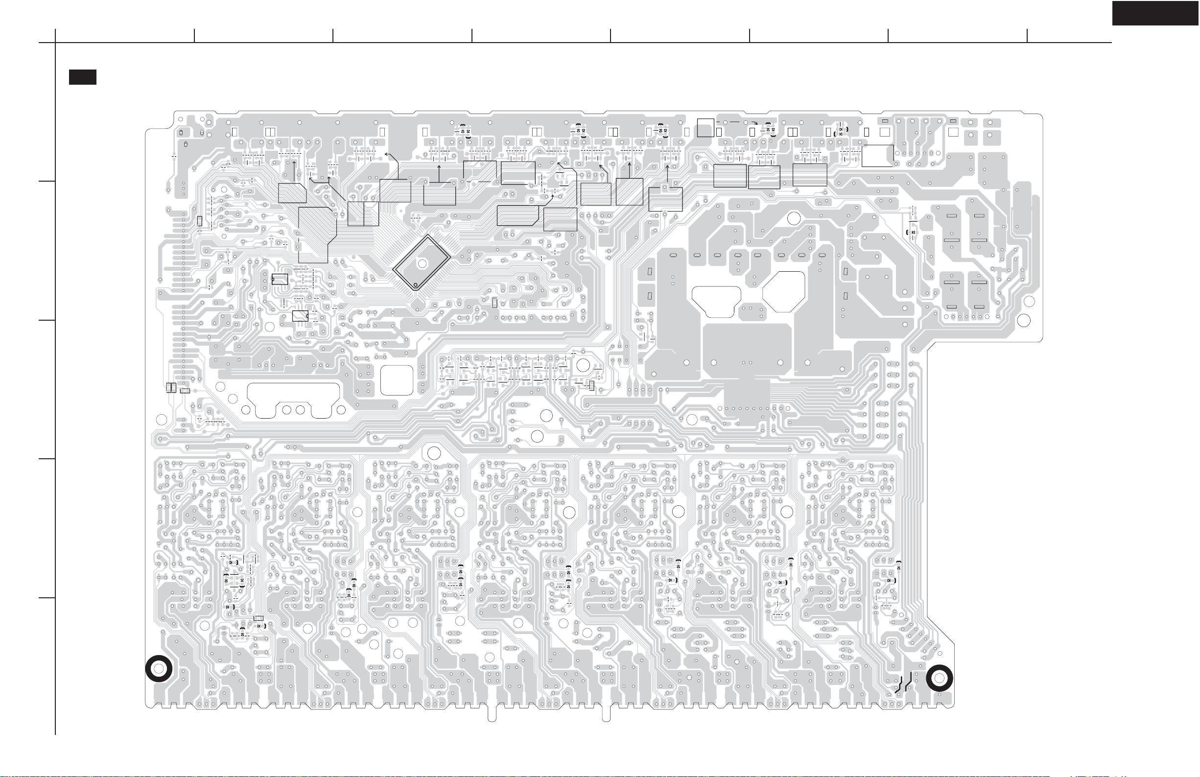
TX-SR506
A
PRINTED CIRCUIT BOARD VIEWS-2
U01
1
2
AMPLIFIER PC BOARD (NAAF-9419)
Soldering side
R5541
R5575
R5501
R5550
R5549
R5580
R5581
R5579
R5823
R5582
R5583
R5576
C5501 C5502
R5577
R5578
R5693
R5692
R5691
R5500
BCDEFGH
C5708
R5532
D5708
D5718
R5573
R5533
C5533 C5534
R5574
R5534
R6902
R6903
Q6707
D6902
C6911
R5542
1
R5502
R5695
Q5503
C5631
R5631
R5503
R5543
R5694
R5544
R5504
C5591
R5596
R5592
R5598
C5590
R5632
1
R5595
R5594
R5633
R5590
R5689
R5634
R5599
R5597
R5593
R5591
R5690
R5505
R5545
C5505 C5506
R5546
R5506
R5507
C5507 C5508
64
R5547
R5548
80
R5508
R5588
R5587
R5513
C5513
1
R5553
D5705
R5560
R5520
D5715
R5561
R5521
C5521 C5522
R5562
R5522
C5523
R5523
R5563
R5564
C5706
R5524
R5566
R5525
C5525 C5526
D5716
R5565
D5706
R5526
D5714
Q5501
24
D5704
R5556
R5515
C5515 C5516
R5555
R5516
R5820
R5557
R5517
C5517 C5518
R5619
Q5609
R5609
Q5608
R5618
R5608
R5558
C5704
R5554
R5514
C5514
40
R5518
R5585
R5519
R5586
C5705
R5559
C5707
D5707
D5717
R5527
C5527
R5567
R5568
C5528
R5528
C5529 C5530
R5529
R5569
R5570
R5530
C5531
R5531
R5571
C5532
R5572
Q5630
3
R5824
R5825
R5826
R5814
R5813
R5680
R5682
R5681
R5630
R5610
R5600 R5601 R5602 R5603 R5604 R5605
Q5600 Q5601
Q5610 Q5611
R5620
R5612
R5611
Q5602 Q5603 Q5604 Q5605
Q5612 Q5613 Q5614
R5621
R5622
R5613
R5623
R5614
R5624
Q5615
R5615
R5625
R5606
Q5606
R5616
Q5616
R5626
R5607
Q5617
Q5607
R5627
R5617
R5821
Q5700
C5700
P6011A
4
R6702R6704
R6706
D6702
D6703
Q6701Q6702
D6704
R6721
Q6703
D6701
R5822
D6016
R6701
R6708
R6709
R6710
C6703
R6145
R6155
D6005
D6015
R6195
R6144
R6154
D6014
D6004
R6194
R6143
R6153
D6013
D6003
R6193
R6142
D6002
D6012
R6152
R6192
R6141
R6151
R6191
D6001
D6011
R6140
R6150
D6010
D6000
R6190
R6196
R6146
R6156
D6006
5
Page 19
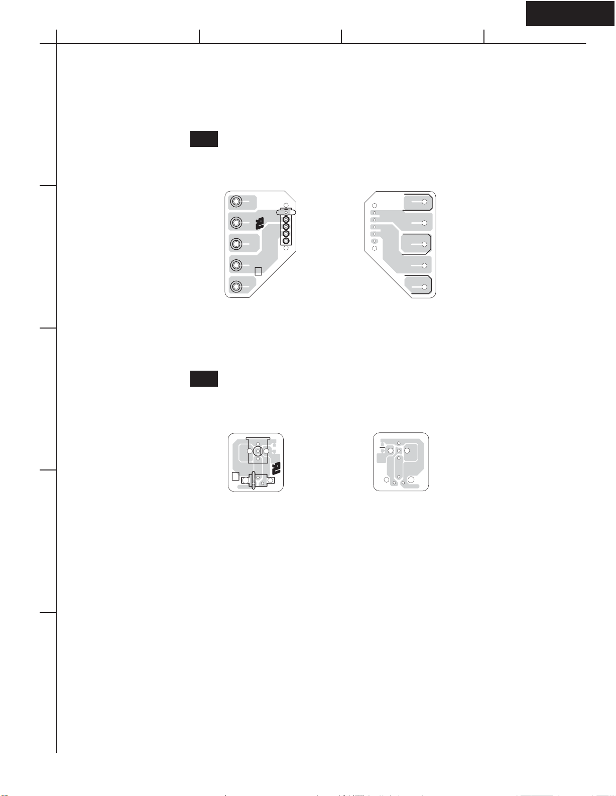
TX-SR506
A
PRINTED CIRCUIT BOARD VIEWS-3
1
U02
2
TRANS. SEC. TERMINAL PC BOARD
(NAPS-9420)
Component side
NCPS-9420
25139420
P17P18P19
0
P15P16
BCD
Soldering side
JL6952A
GRN
BLK
YEW
U03
3
THERMAL SENSOR PC BOARD
(NAETC-9421)
Component side
NCETC-9421
25139421
0
JL6402A
Q6380
Q6380A
Soldering side
C6630
4
5
Page 20
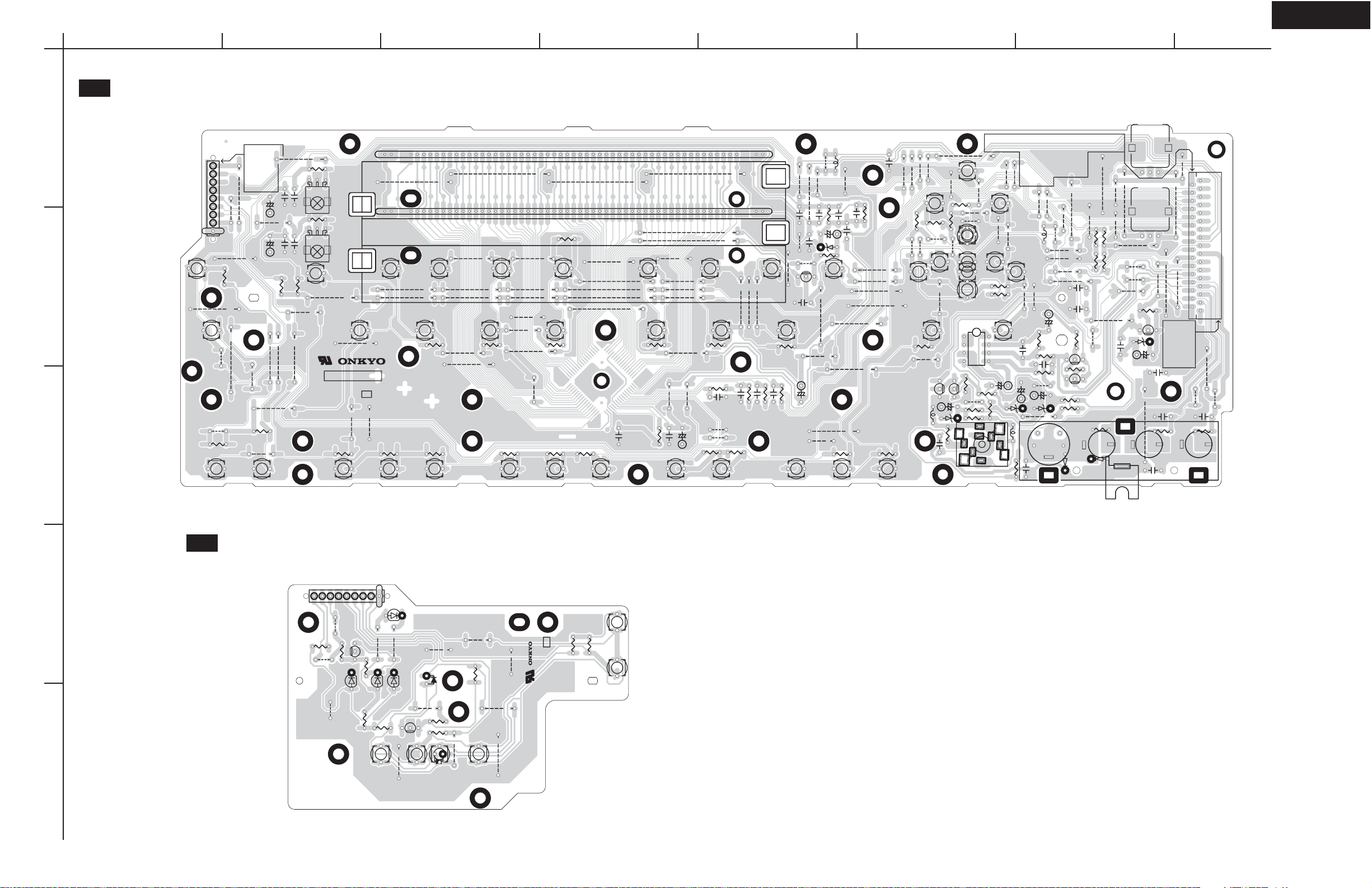
TX-SR506
A
PRINTED CIRCUIT BOARD VIEWS-4
U10
1
2
3
DISPLAY PC BOARD (NADIS-9430)
Component side
R7101
J7011
9
J7192
7
J7064
1
J7063
J7056
15
MULTI CH
20
17
12
J7059
9.LEDZONE2
8.LEDSTBY
7.OPEN
6.GNDDG
5.+5VDIS
4.LEDPURE
3.KEY0_2
2.KEYINT0
1.GNDDG
C7045
J7193
C7041
7
J7060
J7058
R7102
J7057
S7104
J7061
7
C7046
10
C7042
R7045
15
15
J7062
12
6xx
S7102
JL7101A
MULTI CH
S7101
J7012
R7013
S7106
BCDEFGH
22.KEYINT0
04.V4V
05.GNDV4
06.V4_L
07.GNDV4
08.V4_R
09.+15VA
10.MICOUT
11.-15VA
12.MICMUT
13.+5VDIS
J7150
RETURN
7
7
J7144
R7408
R7405
D7411
C7304
7
L7031
J7143
R7407
7
J7147
10
14.MICDET
15.GNDDG
16.VOLB
17.VOLA
18.-VP
19.FLAC2
20.KEYINT1
21.FLAC1
J7151
7
J7149
J7161
J7160
J7159
J7181
C7405
J7142
C7411
10
10
C7022
C7021
17
7
P7301
D7301
J7168
12
R7409
R7411
R7412
23.+3.3VMPU
24.KEY3
17
J7169
10
R7021
J7163
R7023
J7157
Q7403
R7410
Q7404
R7303
E7301
J7182
J7166
J7164
R7022
R7024
C7031
D7302
S7002
6xx
7
33
5xx
10
J7183
20
J7175
J7176
25.KEY2
26.KEY1
27.KEY0
28.FLDSDO
29.FLDCLK
30.FLDCS
31.FLDRST
32.REMIN
33.OPEN
J7101
20
30
J7177
20
15
10
P701B
1
12
J7178
J7054
J7053
C7301C7302
R7301R7302
20
S7001
7
J7167
7
J7162
12
J7158
J7156
7
J7155
R7033
Q7033
12
D7033
C7033
C7305
22
J7170
C7303
J7191
R7041
J7065
C7047
C7043
J7066
15
15
S7130
10
5xx
6xx
R7046
U7042
6xx
R7042
U7041
5xx
DVD
5xx
Q7001
J7072
15
J7071
NCDIS-9430
25139430B
J7070
TONE
R7114
S7148
S7129
10
Q7002
12
1
J7069
01.OPEN
02.LEDSTBY
03.GNDV4V
7
R7123
R7124
J7134
Q7005
S7150
J7136
S7157
J7131
J7137
R7403
ENTER
Q7401
R7413
R7414
P7401
J7145
7
7
S7153
17
J7138
S7158
S7151
R7406
J7135
R7127
R7128
S7159
1
RETURN
C7401
R7404
J7140
ENTER
7
D7412
J7141
J7146
7
7
S7160
7
J7152
S7152
C7404
C7402
C7412
L7401
R7401
7
J7117
J7050
L7032
10
17
J7115
J7119
C7016
J7113
R7001
10
J7116
J7112
Q7004
C7001
CD
J7195
C7013
C7010
J7106
7
C7015
C7017
J7109
J7118
17
S7113
10
J7107
7
R7008
PHONO
R7115
S7132S7134S7136
7
C7012
D7002
J7120
J7196
15
S7126
R7113
J7089
22
J7076
12
S7124
J7083
17
J7082
17
S7125
R7112
12
J7079
15
J7073
MOVIE/TV
R7120
S7142
J7077
S7128
J7075
17
J7074
17
S7127
10
TONE -
R7122
S7146
TONE +
R7121
S7144
J7080
J7081
J7085
J7084
J7087
J7086
30
J7100
R7110
12
R7111
J7095
J7093
J7091
J7090
GAME
R7118R7119
C7007
S7138S7140
S7122
15
15
S7123
10
10
15
7
J7078
MUSIC
J7114
30
J7099
J7098
S7120
J7097
TAP E
S7119
C7009
R7006
TAP E
J7096
J7094
J7092
R7109
7
J7108
DISPLAY
10J7088
J7104
J7194
7
C7008
12
12
12
12
15
22
27
27
22
S7118
R7108
TUNER
TUNER
S7117
R7005
C7005
DIGITAL IN
30
30
30
CD
S7116
15
15
15
J7111
S7115
J7110
J7105
R7107
R7004
C7002
J7103
J7102
C7004
R7116R7117
C7003
R7003
R7002
DIMMER
C7011
C7014
15
J7124
J7123
J7122
J7067
R7007
15
TUNING MODEMEMORY
C7032
12
12
R7130
S7164S7166
7
10
J7130
J7129
J712810J7127
S7156
J7139
R7125
R7126
S7149
J7009
S7155
J7125
J7126
S7154
S7162
SET UP
C7403
D7401
L7402
R7129
J7197
7
J7133
Q7007
C7421
10
R7402
15
17
S7161
SET UP
U11
SWITCH PC BOARD (NADIS-9431)
Component side
4
R7151
J7211
JL7101B
J7212
Q7152
R7158
D7152
J7204
5
R7157
6xx/STBY
R7154
D7155
S7108
10
J7216
6xx/ZONE2
R7152
D7156
J7217
6xx/STBY
10
J7205
10
D7151
Q7151
5xx/ZONE2
5xx/STBY
J7219
S7110
J7220
D7153
R7156
R7103
6xx/PURE
7
S7107
7
5xx/PURE
D7154
5xx/STBY
10
J7223
6xx/PURE
J7227
R7155
S7109
5xx/PURE
7
7
J7228
J7225
10
12
J7224
1
25139431
NCDIS-9431
R7104
R7105
S7112
ZONE2 OFF
S7114
Page 21
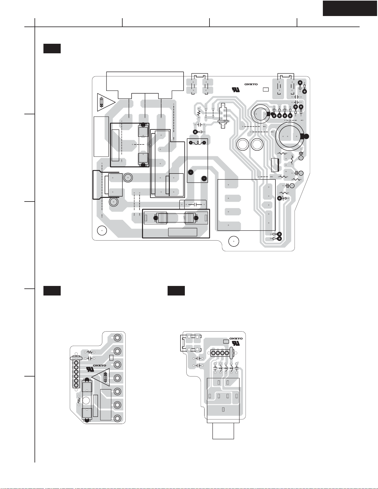
TX-SR506
A
PRINTED CIRCUIT BOARD VIEWS-5
U12
1
2
POWER SUPPLY PC BOARD (NAPS-9432)
Component side
RISK OF FIRE
-REPLACE FUSE
AS MARKED
22
P921A
J902
P922A
P901A
F902
F902A F902B
J903
J90412J905
12
10
T4AL250V
AC CORD
J901
30
BCD
E901
D912
D922
C931
R931
R933
D924
10
D911
D923
C932
P912
S902
J906
20
TRANS IN
P911
C901
C902
D925
E902
R921
J932
RL901
T902
J931
JL901A
NCPS-9432
25139432
J907
C930
J908
1
C911
C921
D921
D930
D931
J910
12
12
C922
R932
Q930
J909
R930
7
C933
98765
R934
D934
4321
D935
D933
F901
8A 125V
F901AF901B
F901CF901D
3
U13
TRANS. SEC. TERMINAL
PC BOARD
(NAPS-9433)
Component side
4
P9590P9591P9595P9596
R9102
C9101
JL9101A
F910B
R9101
F910A
5
NCPS-9433
F910
4A 125V
RISK OF FIRE
1
25139433
-REPLACE FUSE
AS MARKED
P9592P9593P9594
U14
HEADPHONE JACK
PC BOARD
(NAETC-9435)
Component side
E7201
NCETC-9435
25139435
1
JL6605A
C7201
C7202
C7204
L7202
L7203
L7201
C7203
P7201
Page 22
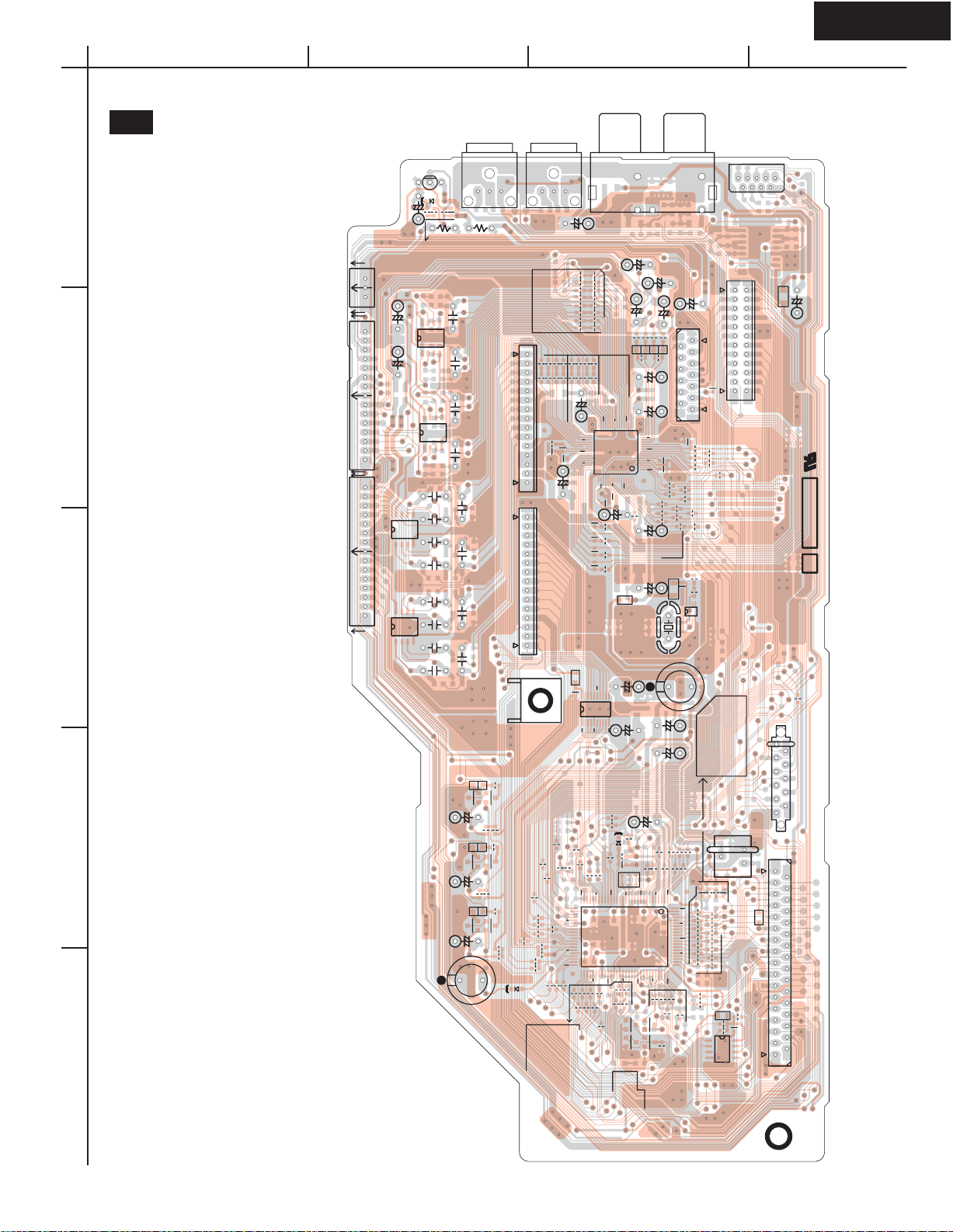
TX-SR506
A
PRINTED CIRCUIT BOARD VIEWS-6
U30
1
2
3
4
5
MICROPROCESSOR
PC BOARD (NADG-9457)
Side-A
P304A
1
P303A
15
1
P302A
15
Q402
C592
1
Q401
1
BCD
Q101
C110
P751A
1
P704A
L134
C139
P101A
C102
24
113
R308
R306
25139457C
R304
NCDG-9457
2
C706
C621
Q153
R695
R693
R691
R682
R687
R685
R690
R701
R700
C620
L153
R153
R152
L747
R151
JL6402B
C151
R608
111
JL101A
1
P701A
33
C413
C591
R771
R761
R623
R714
R713
R773
Q771
R763
Q761
R712
Q752
Q772
D702
Q762
R620
R600
R648
R599
R697
R634
R644
R642
R627
R653
R438
R428
R427
R437
R436
R426
R425
R435
15
R433
R413
P2004A
1
15
1
R641
R650
R658
R660
U131
R423
R403
P2005A
R638
R826
R659
R661
R424
R404
R311
C311
R663
R418
R408
R407
R417
R416
R406
R405
R415
R651
R662
R434
R414
C304
R629
R605
R652
R666
R628
R668
C145
C310
C301
R669
Q152
R625
R670
C313
C334
C337
1
C314
C333
C336
L152
C152
R626
C325 C326
R325
R431
R411
C303
L744
R619
R621
R618
R321
R563
R421
R401
R622
R322
R326
R614
C605
Q756
Q754
R422
R402
R334
R333
R337
R336
D103
R671
R323
C707
C708
C321
R432
R412
C302
R637
1
R673
R324
C322
R674R675
Q301
R312
C604
R732
R318
L313
R314
C748
C747
R303
R301
R611
X701
X171
C702
C705
P131
C323
1
R612
C324
C315
C305
R665
R664
Q755
R317
R315
L311
R655
1
Q753
R722
C306C308
R309
R307
R305
L171
1
R604
Q701
C171
R607
R606
C103
1
R313
1
R672
R316
R677
R676
R302
R319
C316
R173
L173
Q171
R696
R694
R692
R683
R688
R686
R684
1
U132
R102
R103
D105
R109
R110
R111
C109
C408
C407
Q404
1
C406
C414
C762
C412
C411
Q403
C771
C761
C751
C405
C401C402 C403
C404
C772
R772
R762
C613
Q751
C753
1
C422
C421
C424
C423
1
Page 23
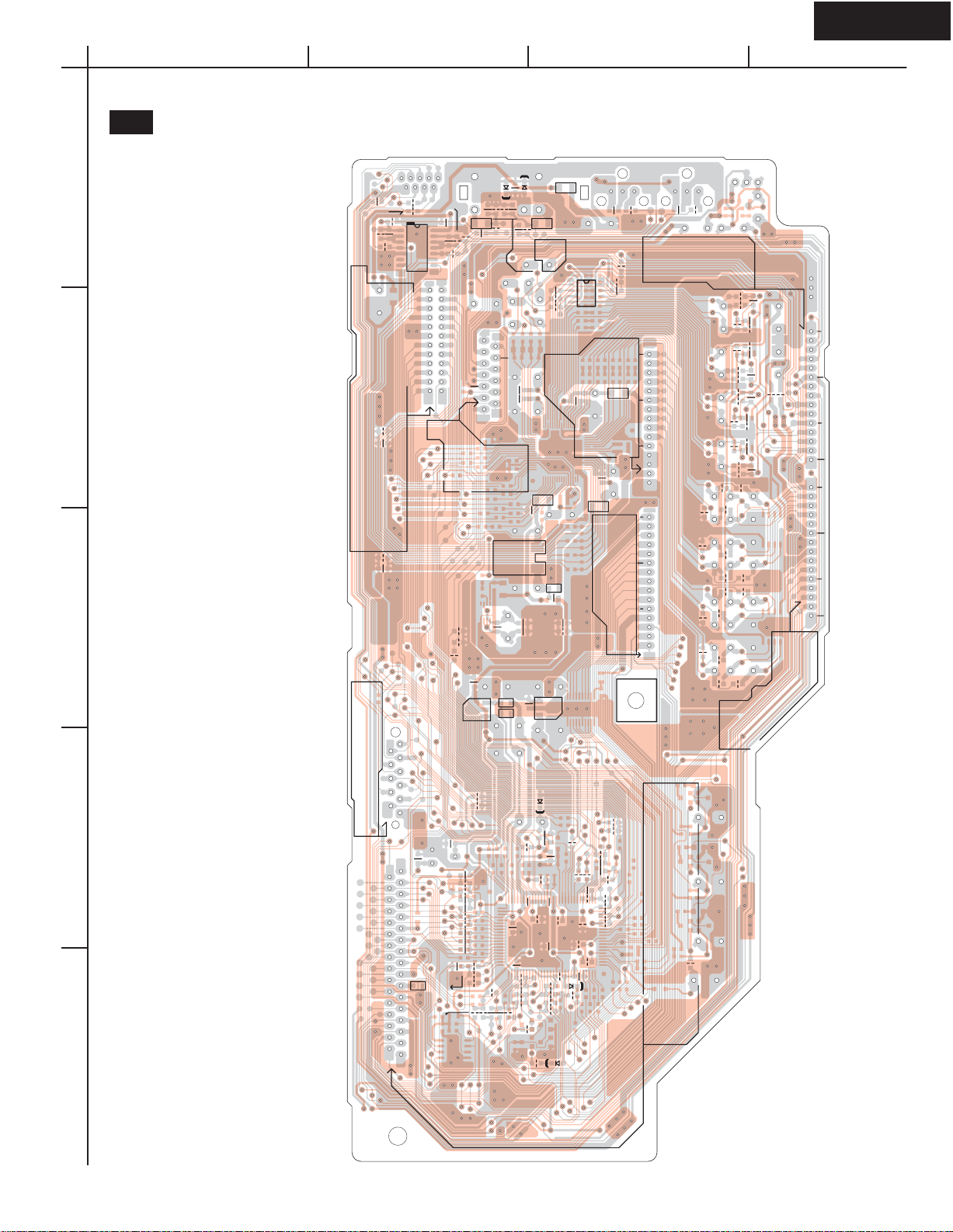
TX-SR506
A
PRINTED CIRCUIT BOARD VIEWS-7
U30
1
2
3
4
5
MICROPROCESSOR
PC BOARD (NADG-9457)
Side-B
C624
R640
R135
R137
C135
R139
01.CX_LRCK
02.CX_SCLK
05.CX_ SD3
06.CX_SD4
07.SAI_SCK
08.SAI_LRCK
09.SAI_SDOUT
10.GND_DSP
11.DSP_RMCK
12.GND_DSP
13.DSPCLKIN
14.DSP_DEC
15.DSPIRQ
16.DSPBSY
17.DSPCE
20.DIGSDI
19.DSP_CLK
22.HDMSEL1
23.HDMSEL2
R339
C210
01.DCKTXD
02.DCKRXD
05.SR-RXD
06.XMLNK
09.XMDACRST
R613
03.CX_SD1
04.CX_SD2
R340
C211
18.DSPRST
21.DIGSDO_DSP
24.HDMSEL3
03.DCKDET
04.SR-TXD
07.XMANT
08.XMRST
10.XM/SR-SEL
11.GNDDG
TO-XM/SR/IPOD
10
20
30
BCD
L133
D706
R138
1
Q131
TO-HDMI
1
C106
1
L746
33
C136
R140
C140
L131
C133
R136
1
11
13
21
24
11
R702
R689
R828
9.TU_R
8.GNDTU
R107
R106
C107
C612
R679
R680
7.TU_L
6.GNDTU
5.+12VTU
4.SD
3.STEREO
2.PLLSDA
1.PLLDCL
R104
Q702
THERMAL
C610
C611
R721
C701
R678
1
13.RDSDAT
12.RDSDAT
11.GNDTU
10.-12VTU
Q746
R567
R568
C634
R719
R720
C635
C619
R699
R698
C618
C617
C616
R703
R704
R705
R706
R133
R171
L741
L743
R601
C745
C602
C307
C104
L302
C173
C172
C601
R723
C134
R609
C608
C625
C146
R134
C317
R338
C709
D601
Q601
R610
C614
R724 D701
D705
C131
R131
R132
C341
R351
R341
09.VDSWS7
08.VDSWS8
07.GNDV4V
06.V3V
05.+5VA
R617
R108
R707
R708
R709
R710
L132
C132
1
C603
C309
L742
C744
R615
R633
Q703
R564
R647
Q341
02.+5VD
01.GNDDG
L304
R631
D104
R105
C141
15.VDSWS1
14.VDSWS2
13.VDSWS3
12.VDSWS4
11.NC
10.VDSWS6
L303
04.GNDA
03.GNDA
C312
11.APOWER
06.SPRLSB
05.SPRLB
R649
C609
R141
R342
R352
C342
14.+10S
13.POFF
12.POFF2
09.HPDET
08.SPRLF
07.SPRLCS
04.+5VDIS
03.-VP
02.FLAC2
R565
R566
R632
C607
C606
R635
C615
R630
R646
R639
R645
R643
C142
R142
08.MICOUT
02.TU_L
03.GND_TU
04.TU_R
05.V3_L
06.GNDV4
07.V3_R
09.RTAD
R478
R458
C428
C418
R468
R448
R447
15
C417
R467
R477
C427
R457
R476
R456
C426
C416
R446
R445
C415
R465 R466
R475
R455
C425
R452
R472
R442
R441
R451
R471
R454
R474
R444
115
R443
R711
TO-VIDEO
1
15.FANCTRL
10.VPOWER
01.FLAC1
20.MICDET
21.+5VDIS
24.MICOUT
To-FRONT
01.RI
01.OPEN
02.REMIN
03.FLDRST
04.FLDCS
05.FLDCLK
06.FLDDO
07.KEY0
08.KEY1
09.KEY2
10.KEY3
11.+3.3S
12.KEYINT0
13.FLAC1
14.KEYINT1
15.FLAC2
16.-VP
17.VOLA
18.VOLB
19.GNDDG
22.MICMUT
23.-15VA
25.+15VA
26.V3_R
27.GNDV4
28.V3_L
29.GNDV4
30.V3V
31.GNDV4V
32.LEDSTBY
33.OPEN
10.LTAD
11.DAC_SR
R462
R464
R473
11.PROTECT
12.SEC1H
13.VOLH
14.AMUT
15.Z2MUT
12.DAC_SL
R453
13.DAC_SBR
14.DAC_SBL
15.SBZ2MUT
R591
R592
TP-SBR
TP-SBL
R461
R463
09.VOLDAT
10.VOLCLK
TP-SR
TP-SL
TP-FL
TP-FR
TP-S/W
TP-C
01.DAC_FR
02.DAC_FL
03.DAC_SW
04.DAC_CT
05.GND_TU
06.-15VA
07.+15VA
08.GNDDG
1
15
1
15
Page 24
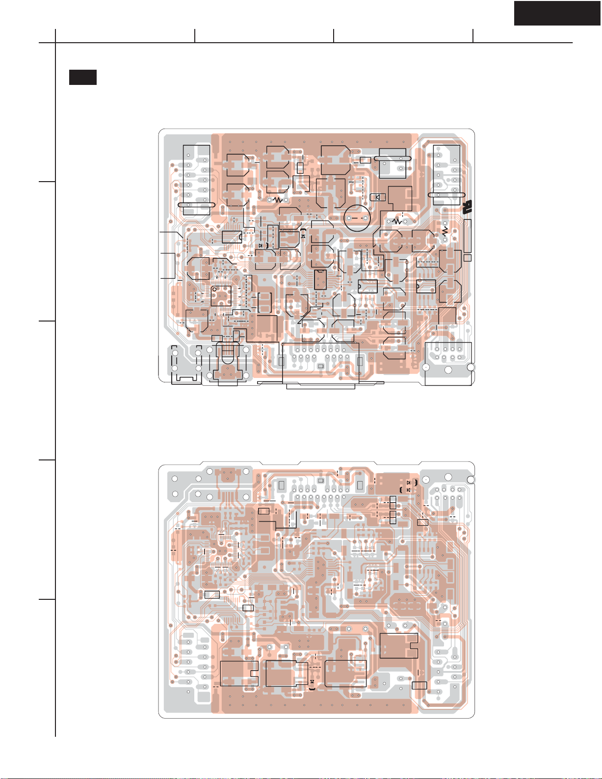
TX-SR506
A
PRINTED CIRCUIT BOARD VIEWS-8
U31
1
2
3
SIRIUS / DOCK TERMINAL PC BOARD (NARF-9458)
<Note>
HT-R560 Only
Side-A
09.XMDACRST
10.XMSRSEL
11.GND_XM
R2012
R2057
R2046
R2045
R2044
R2037
R2011
R2010
L2002
E2001
JL101B
R2015
08.XMRST
R2013
R2014
1
R2043
R2002
R2038
2
C2002
C2034
06.XMLNK
07.XMANT
C2007
R2004
R2001
R2003
L2005
R2054
1
P2001
01.DCKTXD
02.DCKRXD
03.DCKEDT
04.XMSRTXD
05.XMSRRXD
C2043
C2033
R2056
Q2006
R2005
R2071
R2055
R2070
1
D2087
2
R2052
Q2001
C2049
1
R2034
E2003
BCD
01.IPOD_L
JL8002B
R2021
C2025
R2027
C2023
R2025
C202
3
R2048
9
C2079
02.IPOD_R
05.GNDA
06.SR_L
08.+15V
09.-15V
R2031
C2030
C2027
Q2004
1
C2028
R2105
R2110
C2102
R2119
03.XM_L
04.XM_R
07.SR_R
4
R2106
R2108
JL5502B
R2104
R2111
C2044
R2032
R2109
R2107
1
25139458
NCRF-9458
2
C2078
C2077
4
P2002
C2032
R2009
C2006
R2033
C2090
C2092
Q2013
Q2012
R2007
C2005
R2008
R2093
R2092
C2004
L2004
C2045
3
C2047
C2008C2009
R2006
C2040
X2001
R2062
R2061
R2060
R2047
C2100
R2066
C2060
C2103
R2051
R2050
R2053
R2063
C2091
L2083
Q2011
C2061
Q2002
D2088
1
3
C2089
R2073
C2086
01.GND_XM
R2072
Q2072
C2017
R2019
C2018
C2022
C2087
C2088
C2021
R2020
03.IPOD_V02.+12V_XM
L2082
R2122
1
C2104
C2026
R2022
R2120
R2123
R2121
D2086
C2024
R2028
R2026
L2081
3
Q2003
P2080
Side-B
R2089
R2116
R2065
R2125
D2085
R2064
R2127
R2091
R2126
R2118
C2084
R2117
C2036
C2035
R2086
R2024
R2085
R2023
C2038
R2030
Q2008
R2080
R2029
C2037
R2088
R2087
C2081
C2082
D2083
D2082
R2076
L2006
C2031
L2003
01.GND_XM
02.+12V
03.IPOD_V
Q2005
R2040
R2049
R2074
03.XM_L
04.XM_R
07.SR_R
01.IPOD_L
02.IPOD_R
05.GNDA
06.SR_L
08.+15V
09.-15V
C2085
C2097
C2083
C2042
R2079
4
R2078
11.GND_XM
10.XMSRSEL
9.XMDACRST
5
4.XMSRTXD
5.XMSRRXD
6.XMLNK
7.XMANT
8.XMRST
C2001
L2001
3.DCKEDT
C2003
C2012
C2013
Q2007
R2075
1.DCKTXD
2.DCKRXD
C2010
C2011
L2007
C2039
L2086
R2081
R2082
R2083
R2115
C2101
Q2009
R2090
C2048
C2046
Page 25
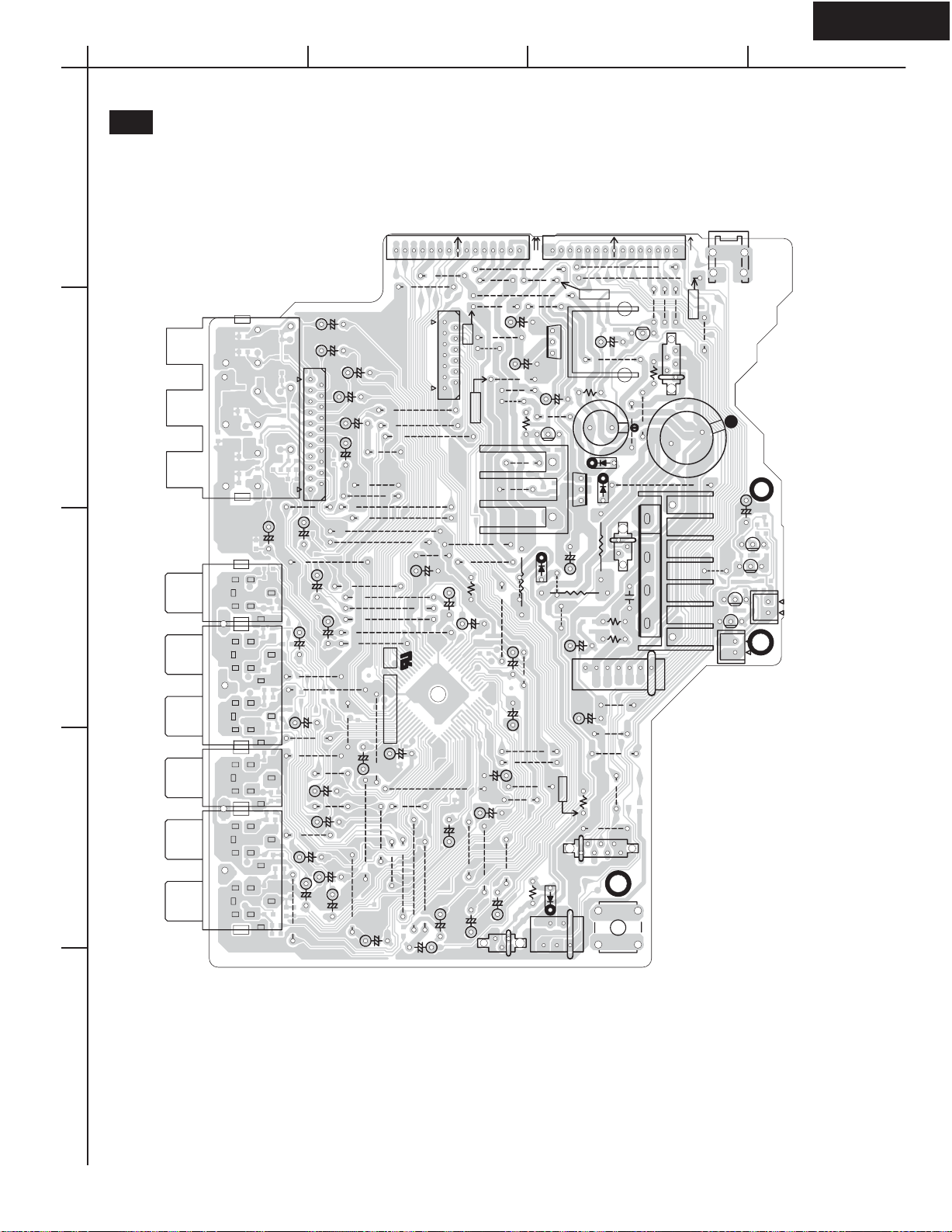
TX-SR506
A
PRINTED CIRCUIT BOARD VIEWS-9
U36
1
2
3
4
VIDEO PC BOARD (NAVD-9467)
Component side
P2004B
5.+5V
7.VG
C3047
15
J3010
C3034
C3046
C3045
25
25
15
10
C3040
J3012
17
C3048 C3049
20
20
C3044
10
J3046
22
J3013
22
C3018
15.S1
J3084
J3036
J3032
J3031
C3003
7
J3011
14.S2
J3047
20
J3035
J3034
J3033
J3014
12
6.V4V
13.S3
17
17
J3041
C3001
J3015
12.S4
20
12
1
NCVD-9467
J3020
J3019
7
10
J3016
1
P3004
P3001
C3007
P3003
P3002
J3002
J3001
J3045
17
C3081
12
17
J3007
12
10
15
C3082
C3033
P3005
C3055
J3009
J3008
J3006
C3041
10
C3054
J3037
C3004
10
J3004
7
7
P3007A
25
J3003
C3037
C3036
BCD
10
12
J3081
4.AG
3.AG
2.+5V
9.S7
11.S5
10.S6
J3052
J3051
J3050
J3044
J3043
J3042
22
J3038
C3006
20
25139467B
17
J3017
J3018
20
25
C3060
8.S8
1.MG
J3083
J3040
7
C3024
C3061
J3054
J3055
J3057
7
J3059
J3060
10
C9023
J3061
10
+10S
C9025
J3074 J3065
J3062
10
J3092
Q9031A
R3038
C3011
C3022
J3023
15
JL6017A
+12V
+10V
15
J3030
J3091
7
17
C3017
10
J3024
J3088
12
J3063
J3089
J3025
C3021
C3085
R9035
C3013
J3028
J3027
J3026
7
7
7
POFF
R9011
12
C3009
C3084
P2801A
22
J3022
12
GND
+5V_VD
J3039
J3058
7
7
D9022
R9030
J3029
SEC2
+12VD
JL901B
20
7
Q9022
C9032
J3087
7
SEC2S3S3
12
10
MPUGND
+10S
D9013
22
J3090
J3077
FLAC
POWERD
Q9020
R9032
C9013
FLAC
C9014
+10VS
POFF
R9033
+12VD
+5VDSP
Q9022A
R9001
Q9031
C9030
GND
+10VS
C9005
12
D9002
R9031
7
J3079
SPRLB
J3021
10
JL9102B
POWERD
R9012
R9013
J3078
J3086
SPRLSB
SPRLCS
E9002
J3068
D9001
J3073
GND
+12XM
IPOD
JL8002A
J3066
7
J3067
C9001
C9012
7
10
SPRLF
Q9001
10
J3085
10
D9011
-+
MPUGND
HPDET
R9029
J3064
AC
MPUGND
7
22
7
J3069
D9011A
7
J3070
JL9101B
27
J3071
15.FCTRL
JL8001A
P9110
P2005B
APOWER
7
14.+10S
GND_HD
+12V_HD
GND_HD
+12V_HD
GND_HD
22
Q9102
Q9101
J3072
J3080
E9001
13.POFF
12.POFF2
C9011
C9101
11.APOWER
Q9112
10.VPOWER
Q9111
5.SPRLZ2
9.HPDET
8.SPRLF
3.-VP
2.FLAC2
4.+5DIS
7.SPRLSB
6.SPRLSB
P9111
1.FLAC1
5
Page 26
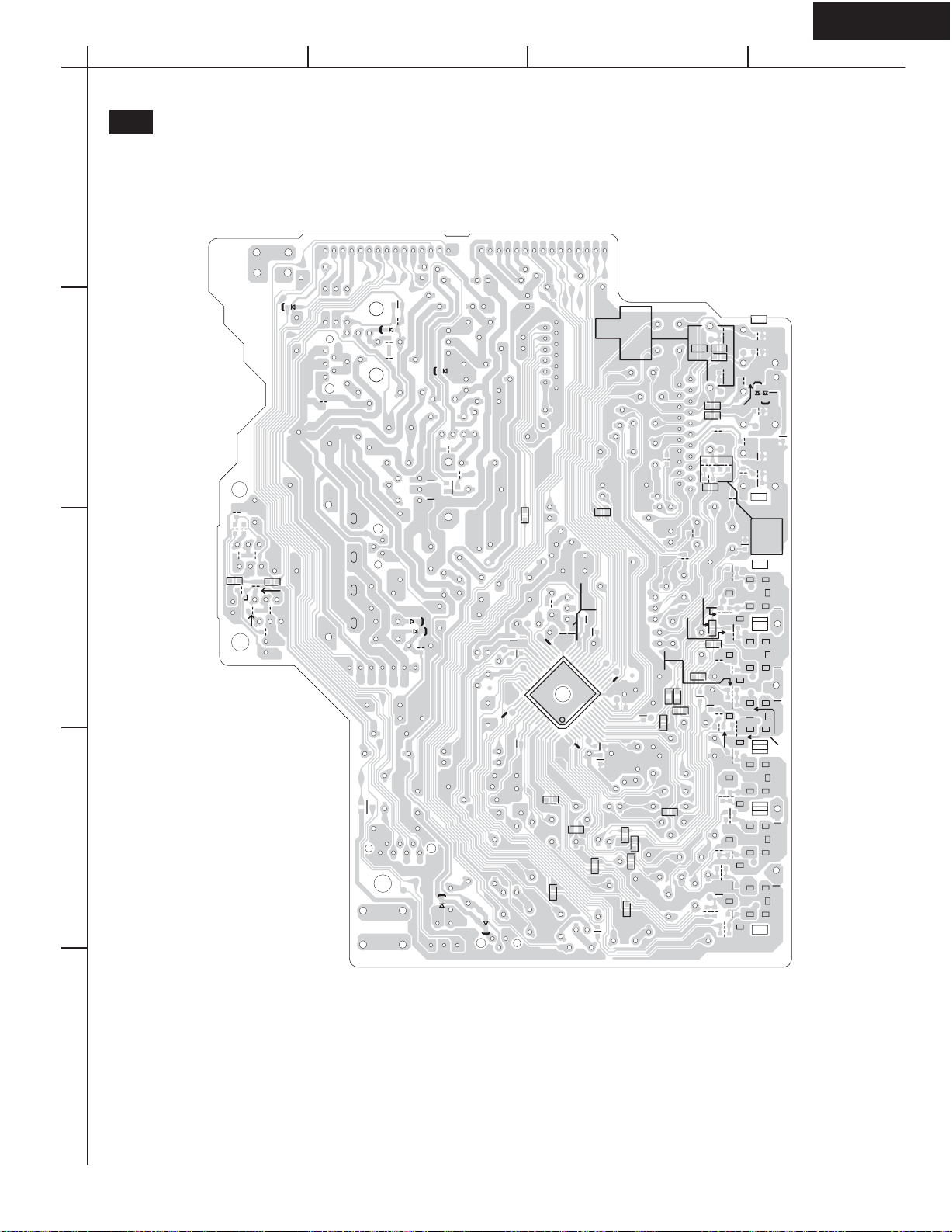
TX-SR506
A
BCD
PRINTED CIRCUIT BOARD VIEWS-10
U36
1
2
3
4
VIDEO PC BOARD (NAVD-9467)
Soldering side
Q9002
R9002
C9006
R9004
D9005
D9014
R9003
R9112
R3065
R9115
R9105
D9016
R9102
R9114
R9111
R9113
R9104
R3064
R9101
R9036
R9103
D9015
R9014
D9023
C9033
D9012
Q9021
C9031
R9024
GD
R9025
5V
C3086
49
D9017
GV
5V
4V
GA
GA
S8
R3051
R3084
C3012
C3089
33
C3023
R3068
S2S3S4S5S6
S7
R3089
R3053
R3072
S1
R3029
C3072
R3063
R3050
R3062
R3026
C3073
R3061
R3060
R3044
R3001
R3074
R3052
C3091
C3092
C3005
C3087
17
C3010
Q3001
C3019
1
C3002
R3075
R3067
C3014
R3066
R3069
R3007
R3022
C3066
C3008
R3073
C3090
R3070
R3071
R3086
R3056
R3054
R3085
C3042
R3025
R3055
C3064
R3058
R3057
C3015
R3004
R3011
C3067
R3009
C3038
C3035
R3016
R3006
R3059
R3013
R3081
R3023
R3014
R3082
R3017
R3012
R3005
R3002
C3083
R3083
R3020
R3019
C3063
R3028
C3062
R3041
R3042
R3015
R3024
R3018
R3027
C3088
D3028
R3003
R3010
R3031
R3030
D3029
R3043
C3070
R3045
C3069
C3068
R3008
R3021
C3043
C3050
R3046
C3056
C3030
C3039
C3065
C3032
C3031
5
Page 27
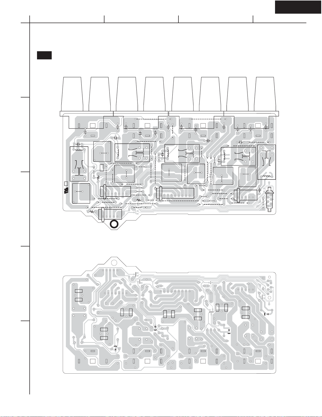
TX-SR506
A
BCD
PRINTED CIRCUIT BOARD VIEWS-11
U37
1
2
3
SPEAKER TERMINAL PC BOARD (NATRM-9468)
Component side
RL6600
J6604
15
25
JL6605B
R6690
HPL
J6670
C6650
20
J6636
7
J6637
L6601
J6638
J6641
J6643
GND
HPE
HPR
DET
P6601
1
RL6602
25139468
NCTRM-9468
1
SBLSP
SLSP
J6851
LSP
C6642
C6651
P6602
L6600
R6692
JL6600B
12
J6600
+24V
J6633
J6632
12
J6634
J6635
C6600
10
C6652
C6602
J6630
7
L6602
J6631
17
CSP
SRSP
SBRSP
RSP
25
R6691
J6669
10
J6639
J6640
12
J6645
J6646
J6642
10
12
C6640
J6649
P6603
CS
LS
J6651
J6671
C6653
C6643
J6652
7
J6620
15
7
L6604
J6656
15
J6659
30
SLS
SBLS
17
J6653
17
J6660
J6654
20
J6657
RL6605
C6605
J6655
J6661
J6658
25
C6644
J6662
J6625
P6604
J6666
JL6604B
J6663
C6656
C6645
20
L6606
J6626
L6605
15
10
SPBL
SPBR
12
SPBLE
C6655
J6665
SPBRE
SPBRE
C6646
15
RL6607
C6607
J6664
7
JL9102A
25
C6654
C6641
J6668
10
17
C6603
GND
J6619
JL6603B
J6644
SBRS
RL6603
SRS
RS
J6647
J6648
L6603
25
7
+24V
Soldering side
Q6601
R6693
Q6603
R6606
R6616
R6615
Q6604
D6607
R6605
D6605
R6611
Q6602
R6601
D6603
R6613
R6604
R6614
R6603
4
5
R6602
R6612
R6600
R6610
D6600
Page 28
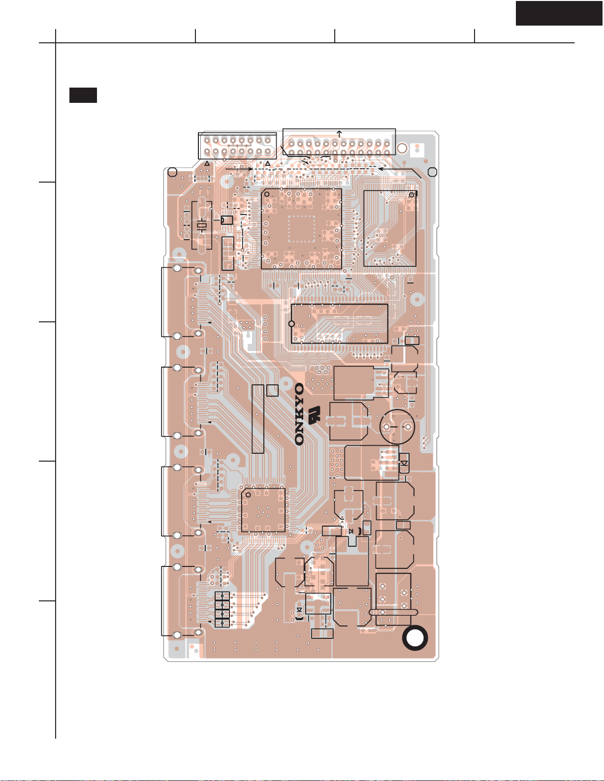
TX-SR506
A
BCD
PRINTED CIRCUIT BOARD VIEWS-12
U42
1
2
3
HDMI PC BOARD (NAHDM-9475)
Side-A
R8003
C8021
R268
L204
X202
P8001
L312
C236
1
L241
P8002
R266
Q202
R8002
R8005
R8006
P202
R270
R8007
R8009
R8008
R8011
R8012
R269
TP36
R8001
R200
C202
R207
C203
C204
C242
C222
1
TP32
TP01
1
R8027
R8929
C238
R272
C239
TP7
C223
TP41
HDMSEL2
HDMSEL1
L201
1
C295
R260
R259
R257
R256
R255
R254
R252
R251
R250
R209
R253
Q282
C8072
C8073
C8074
HDMSEL3
TP33
TP31
L203
Q281
TP40
P704B
109
25
C227
72
R221
28
C246
C8071
R265
Q201
TP38
R261
1
C207
1
Q8007
R8019
41
Q8003
Q8001
C8075
Q8006
R280
D8007
Q8002
TP9
TP11
L8007
C8198
GND
GND
GND_V
C8016
TP6
L8008
TP22
C8014
1
C8022
R8020
TP13
R8028
R8013
R8015
C8020
R8014
R8017
P8003
R8018
R8010
R8004
1
NCHDM-9475
25139475A
61
4
R8016
TP15
TP4
R8022
R8023
R8024
TP02
L8001
L8002
L8003
21
C8018
C8015
TP14
C8017
D8006
C8013
C8019
TP20
P8004
L8004
TP8
TP5
D8001
C8077
L8015
C8199
L8014
TP10
C8076
JL801B
+12V
+12V
5
Page 29
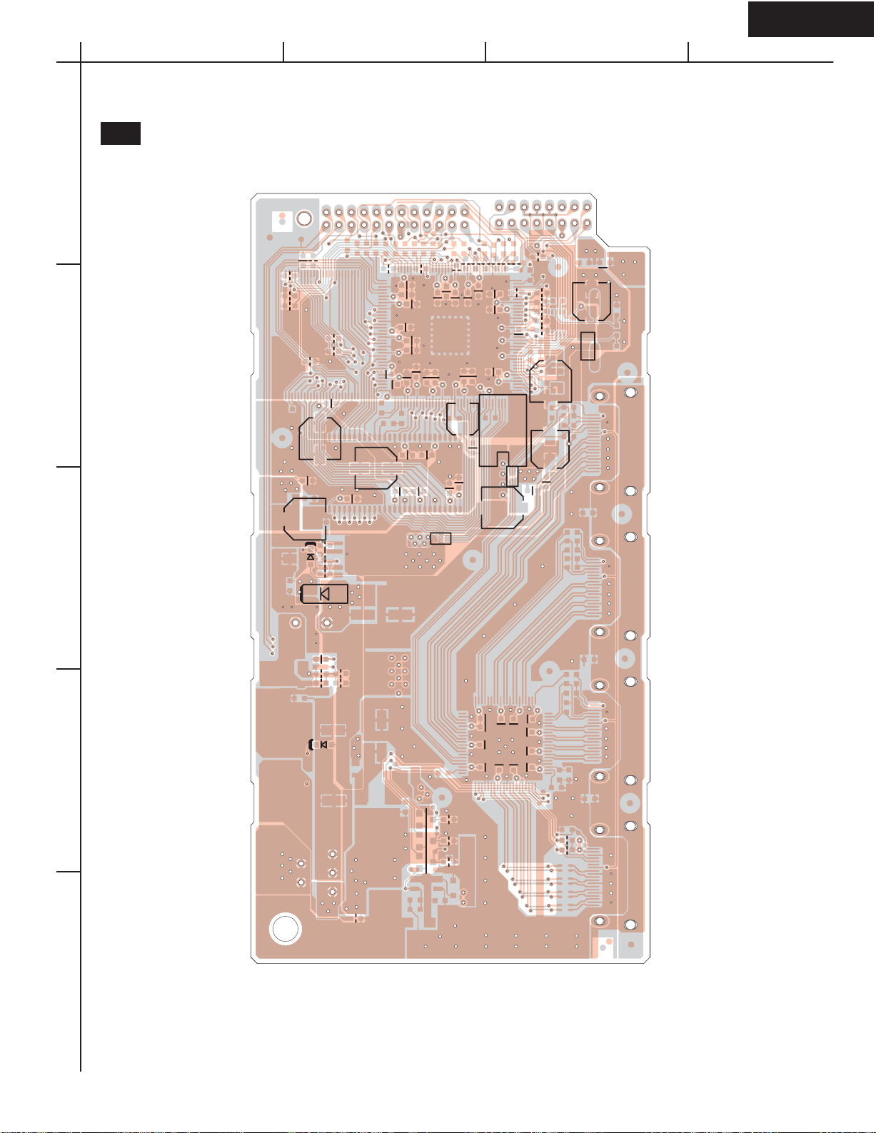
TX-SR506
A
BCD
PRINTED CIRCUIT BOARD VIEWS-13
U42
1
2
3
HDMI PC BOARD (NAHDM-9475)
Side-B
C283
R286
C282
C217
C281
C289
R8936
R8935
R8937
R8938
R273
C284
C231
C230
C213
C228
C219
R282
R283
R284
R281
R285
R287
TP34
C218
D8004
C288
C290
R258
C226
C287
C229
C209
C291
L282
C214
C212
C211
C225
TP39
R288
C208
C232
C8067
C286
R262
C215
C285
R263
C224
C8068
TP30
TP37
C216
C206
C201
C233
C205
L202
R264
R267
Q8008
C235
R290
C221
R201
C243
R289
R208
C234
R202
R203
R204
R205
R206
C8079
C237
TP35
L205
C241
C8066
C245
D8003
C8078
R8933 R8934
D8002
4
R8931R8932
C8010
C8011
R8021
TP3
Q8004
Q8005
Q8009
TP12
C8009
C8008
C8007
C8006
TP17
TP18
TP19
C8004
R8029
R8030
R8039
C8005
TP16
C8012
C8001
C8002
C8003
R8025
R8026
TP21
5
Page 30
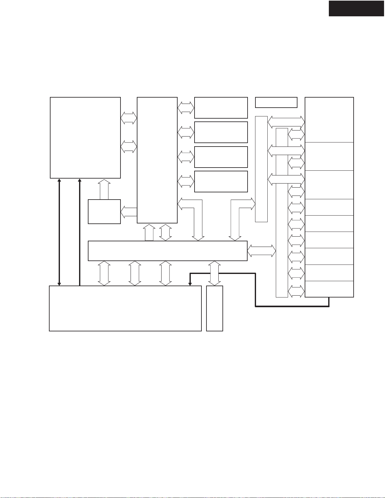
IC BLOCK DIAGRAMS AND TERMINAL DESCRIPTIONS-1
Q201 : D788E001BRFP266 (Floating-Point Digital Signal Processor)-1/5
BLOCK DIAGRAM
TX-SR506
C67x + CPU
Program
INTI/O
Program
32K Bytes
Fetch
256
Cache
D1
Data
R/W
D2
Data
R/W
64
64
256
Memory
Controller
High-Performance
Crossbar Switch
32
DMPPMP
CSP
3232
32
256
256
256
256
32
Program/Data
RAM
256K Bytes
Program/Data
ROM Page1
256K Bytes
Program/Data
ROM Page2
256K Bytes
Program/Data
ROM Page3
256K Bytes
32
32
JTAG EMU
32
32
32
McASP DMA Bus
32
McASP0
16 Serializers
32
McASP1
32
32
32
32
32
32
Peripheral Configuration Bus
32
6 Serializers
McASP2
2 Serializers
DIT Only
SPI1
SPI0
I2C0
I2C1
RTI
I/O
Interrupts
Out
dMAX
MAX1MAX032CONTROL
Events
In
EMIF
Peripheral Interrupt and DMA Events
32
PLL
Page 31

IC BLOCK DIAGRAMS AND TERMINAL DESCRIPTIONS-2
Q201 : D788E001BRFP266 (Floating-Point Digital Signal Processor)-2/5
PIN LAYOUT
SPI0_CLK/I2C0_SCL
SPI0_SCS/I2C1_SCL
VSS
SPI0_ENA/I2C1_SDA
EM_OE
DVDD
EM_RW
CVDD
EM_CS[2]
VSS
EM_RAS
EM_CS[0]
EM_BA[0]
VSS
EM_BA[1]
EM_A[10]
DVDD
EM_A[0]
CVDD
EM_A[1]
EM_A[2]
VSS
EM_A[3]
CVDD
EM_A[4]
EM_A[5]
VSS
DVDD
EM_A[6]
EM_A[7]
VSS
CVDD
EM_A[8]
EM_A[9]
EM_A[11]
TX-SR506
DVDD
VSS
SPI0_SIMO
SPI0_SOMI/I2C0_SDA
DVDD
AXR0[0]
VSS
AXR0[1]
AXR0[2]
AXR0[3]
VSS
AXR0[4]
AXR0[5]/SPI1_SCS
AXR0[6]/SPI1_ENA
AXR0[7]/SPI1_CLK
CVDD
VSS
DVDD
AXR0[8]/AXR1[5]/SPI1_SOMI
AXR0[9]/AXR1[4]/SPI1_SIMO
CVDD
VSS
AXR0[10]/AXR1[3]
AXR0[11]/AXR1[2]
CVDD
VSS
AXR0[12]/AXR1[1]
AXR0[13]/AXR1[0]
DVDD
AXR0[14]/AXR2[1]
AXR0[15]/AXR2[0]
ACLKR0
VSS
AFSR0
ACLKX0
AHCLKR0/AHCLKR1
AFSX0
108
107
106
105
109
110
111
112
113
114
115
116
117
118
119
120
121
122
123
124
125
126
127
128
129
130
131
132
133
134
135
136
137
138
139
140
141
142
143
144
123456789
104
103
999897969594939291908988878685848382818079787776757473
102
101
100
144-pin RFP
101112131415161718192021222324252627282930313233343536
72
71
70
69
68
67
66
65
64
63
62
61
60
59
58
57
56
55
54
53
52
51
50
49
48
47
46
45
44
43
42
41
40
39
38
37
VSS
EM_CKE
EM_CLK
VSS
DVDD
EM_WE_DQM[1]
EM_D[8]
CVDD
EM_D[9]
EM_D[10]
VSS
EM_D[11]
DVDD
EM_D[12]
EM_D[13]
CVDD
EM_D[14]
EM_D[15]
VSS
CVDD
EM_D[0]
EM_D[1]
DVDD
EM_D[2]
EM_D[3]
VSS
EM_D[4]
EM_D[5]
CVDD
EM_D[6]
DVDD
EM_D[7]
VSS
EM_WE_DQM[0]
EM_WE
EM_CAS
VSS
AMUTE0
AMUTE1
AHCLKX1
AHCLKX0/AHCLKX2
VSS
CVDD
ACLKX1
DVDD
ACLKR1
AFSX1
AFSR1
VSS
VSS
RESET
CVDD
CLKIN
VSS
TMS
TRST
CVDD
OSCIN
OSCVSS
OSCOUT
VSS
PLLHV
OSCVDD
TDI
TDO
VSS
DVDD
EMU[0]
CVDD
EMU[1]
TCK
VSS
Page 32

IC BLOCK DIAGRAMS AND TERMINAL DESCRIPTIONS-3
Q201 : D788E001BRFP266 (Floating-Point Digital Signal Processor)-3/5
TERMINAL DESCRIPTION
External Memory Interface (EMIF) Address and Control
Pin Name
EM_A[0]
EM_A[1]
EM_A[2]
EM_A[3]
EM_A[4]
EM_A[5]
EM_A[6]
EM_A[7]
EM_A[8]
EM_A[9]
EM_A[10]
EM_A[11]
EM_BA[0]
EM_BA[1]
EM_CS[0]
EM_CS[2]
EM_CAS
EM_RAS
EM_WE
EM_CKE
EM_CLK
EM_WE_DQM[0]
EM_WE_DQM[1]
EM_OE
EM_RW
Pin No.
91
89
88
86
84
83
80
79
76
75
93
74
96
94
97
100
37
98
38
71
70
39
67
104
102
Type
O
O
O
O
O
O
O
O
O
O
O
O
O
O
O
O
O
O
O
O
O
O
O
O
O
Description
EMIF Address Bus
SDRAM Bank Address and Asynchronous Memory
Low-Order Address
SDRAM Chip Select
Asynchronous Memory Chip Select
SDRAM Column Address Strobe
SDRAM Row Address Strobe
SDRAM Write Enable
SDRAM Clock Enable
SDRAM Clock
Write Enable or Byte Enable for EM_D[7:0]
Write Enable or Byte Enable for EM_D[15:8]
SDRAM Output Enable
Asynchronous Memory Read/not Write
TX-SR506
External Memory Interface (EMIF) Data Bus
Pin Name
EM_D[0]
EM_D[1]
EM_D[2]
EM_D[3]
EM_D[4]
EM_D[5]
EM_D[6]
EM_D[7]
EM_D[8]
EM_D[9]
EM_D[10]
EM_D[11]
EM_D[12]
EM_D[13]
EM_D[14]
EM_D[15]
Pin No.
52
51
49
48
46
45
43
41
66
64
63
61
59
58
56
55
Type
IO
IO
IO
IO
IO
IO
IO
IO
IO
IO
IO
IO
IO
IO
IO
IO
Description
EMIF Data Bus [Lower 16 Bits]
Page 33

IC BLOCK DIAGRAMS AND TERMINAL DESCRIPTIONS-4
Q201 : D788E001BRFP266 (Floating-Point Digital Signal Processor)-4/5
TERMINAL DESCRIPTION
McASP0, McASP1, McASP2, and SPI1 Serial Ports
Pin Name
AHCLKR0/AHCLKR1
ACLKR0
AFSR0
AHCLKX0/AHCLKX2
ACLKX0
AFSX0
AMUTE0
AXR0[0]
AXR0[1]
AXR0[2]
AXR0[3]
AXR0[4]
AXR0[5]/SPI1_SCS
AXR0[6]/SPI1_ENA
AXR0[7]/SPI1_CLK
AXR0[8]/AXR1[5]/
SPI1_SOMI
AXR0[9]/AXR1[4]/
SPI1_SIMO
AXR0[10]/AXR1[3]
AXR0[11]/AXR1[2]
AXR0[12]/AXR1[1]
AXR0[13]/AXR1[0]
AXR0[14]/AXR2[1]
AXR0[15]/AXR2[0]
ACLKR1
AFSR1
AHCLKX1
ACLKX1
AFSX1
AMUTE1
Pin No.
143
139
141
2
142
144
3
113
115
116
117
119
120
121
122
126
127
130
131
134
135
137
138
9
12
5
7
11
4
Type
IO
IO
IO
IO
IO
IO
O
IO
IO
IO
IO
IO
IO
IO
IO
IO
IO
IO
IO
IO
IO
IO
IO
IO
IO
IO
IO
IO
O
Description
McASP0 and McASP1 Receive Master Clock
McASP0 Receive Bit Clock
McASP0 Receive Frame Sync (L/R Clock)
McASP0 and McASP2 Transmit Master Clock
McASP0 Transmit Bit Clock
McASP0 Transmit Frame Sync (L/R Clock)
McASP0 MUTE Output
McASP0 Serial Data 0
McASP0 Serial Data 1
McASP0 Serial Data 2
McASP0 Serial Data 3
McASP0 Serial Data 4
McASP0 Serial Data 5 or SPI1 Slave Chip Select
McASP0 Serial Data 6 or SPI1 Enable (Ready)
McASP0 Serial Data 7 or SPI1 Serial Clock
McASP0 Serial Data 8 or McASP1 Serial Data 5 or
SPI1 Data Pin Slave Out Master In
McASP0 Serial Data 9 or McASP1 Serial Data 4 or
SPI1 Data Pin Slave In Master Out
McASP0 Serial Data 10 or McASP1 Serial Data 3
McASP0 Serial Data 11 or McASP1 Serial Data 2
McASP0 Serial Data 12 or McASP1 Serial Data 1
McASP0 Serial Data 13 or McASP1 Serial Data 0
McASP0 Serial Data 14 or McASP2 Serial Data 1
McASP0 Serial Data 15 or McASP2 Serial Data 0
McASP1 Receive Bit Clock
McASP1 Receive Frame Sync (L/R Clock)
McASP1 Transmit Master Clock
McASP1 Transmit Bit Clock
McASP1 Transmit Frame Sync (L/R Clock)
McASP1 MUTE Output
TX-SR506
SPI0, I2C0, and I2C1 Serial Port Pins
Pin Name
SPI0_SOMI/I2C0_SDA
SPI0_SIMO
SPI0_CLK/I2C0_SCL
SPI0_SCS/I2C1_SCL
SPI0_ENA/I2C1_SDA
Pin No.
111
110
108
107
105
Type
IO
IO
IO
IO
IO
Description
SPI0 Data Pin Slave Out Master In or I2C0 Serial Data
SPI0 Data Pin Slave In Master Out
SPI0 Serial Clock or I2C0 Serial Clock
SPI0 Slave Chip Select or I2C1 Serial Clock
SPI0 Enable (Ready) or I2C1 Serial Data
Page 34

IC BLOCK DIAGRAMS AND TERMINAL DESCRIPTIONS-5
Q201 : D788E001BRFP266 (Floating-Point Digital Signal Processor)-5/5
TERMINAL DESCRIPTION
Clocks
Pin Name
OSCIN
OSCOUT
OSCVDD
OSCVSS
CLKIN
PLLHV
Device Reset
Pin Name
RESET
Emulation/JTAG Port
Pin Name
TCK
TMS
TDI
TDO
TRST
EMU[0]
EMU[1]
Pin No.
23
24
25
22
17
27
Pin No.14TypeIDescription
Pin No.
35
19
28
29
21
32
34
Type
I
O
---
--I
---
Type
I
I
I
O
I
IO
IO
Description
1.2-V Oscillator Input
1.2-V Oscillator Output
Oscillator 1.2-V VDD tap point (for filter only)
Oscillator VSS tap point (for filter only)
Alternate clock input (3.3-V LVCMOS Input)
PLL 3.3-V Supply Input (requires external filter)
Device reset pin
Description
Test Clock
Test Mode Select
Test Data In
Test Data Out
Test Reset
Emulation Pin 0
Emulation Pin 1
TX-SR506
Power Pins
Pin Name
Core Supply (CVDD)
IO Supply (DVDD)
Ground (VSS)
Pin No.
8, 16, 20, 33, 44, 53, 57, 65, 77, 85, 90, 101, 123, 128, 132
10, 31, 42, 50, 60, 68, 73, 81, 92, 103, 112, 125, 136
1, 6, 13, 15, 18, 26, 30, 36, 40, 47, 54, 62, 69, 72, 78, 82, 87, 95, 99, 106, 109, 114, 118, 124,
129, 133, 140
Page 35

IC BLOCK DIAGRAMS AND TERMINAL DESCRIPTIONS-6
Q281 : M12L64164A-7TG (1M x 16 Bit x 4 Banks Synchronous DRAM)
BLOCK DIAGRAM PIN LAYOUT
TOP VIEW
CLK
CKE
Address
CS
RAS
CAS
WE
Clock
Generator
Mode
Register
Control Logic
Command Decoder
Row
Address
Buffer
&
Refresh
Counter
Column
Address
Buffer
&
Refresh
Counter
Bank B
Bank A
Row Decoder
Sense Amplifier
Column Decoder
Data Control Circuit
Bank D
Bank C
L(U)DQM
Latch Circuit
Buffer
DQ
Input & Output
VDD
DQ0
VDDQ
DQ1
DQ2
VSSQ
DQ3
DQ4
VDDQ
DQ5
DQ6
VSSQ
DQ7
VDD
LDQM
WE
CAS
RAS
CS
A13
A12
A10/AP
VDD
1
2
3
4
5
6
7
8
9
10
11
12
13
14
15
16
17
18
19
20
21
22
A0
23
A1
24
A2
25
A3
26
27
TX-SR506
VSS
54
DQ15
53
VSSQ
52
DQ14
51
DQ13
50
VDDQ
49
DQ12
48
DQ11
47
VSSQ
46
DQ10
45
DQ9
44
VDDQ
43
DQ8
42
VSS
41
NC
40
UDQM
39
CLK
38
CKE
37
NC
36
A11
35
A9
34
A8
33
A7
32
A6
31
A5
30
A4
29
VSS
28
TERMINAL DESCRIPTION
Pin Name
CLK
CS
CKE
A0 ~ A11
A12 , A13
RAS
CAS
WE
L(U)DQM
DQ0 ~ DQ15
VDD / VSS
VDDQ / VSSQ
NC
Description
Active on the positive going edge to sample all inputs.
Disables or enables device operation by masking or enabling all inputs except CLK , CKE and L(U)DQM.
Masks system clock to freeze operation from the next clock cycle.
CKE should be enabled at least one cycle prior new command.
Disable input buffers for power down in standby.
Row / column address are multiplexed on the same pins.
Row address : RA0~RA11, column address : CA0~CA7.
Selects bank to be activated during row address latch time.
Selects bank for read / write during column address latch time.
Latches row addresses on the positive going edge of the CLK with RAS low.
Enables row access & precharge.
Latches column address on the positive going edge of the CLK with CAS low. Enables column access.
Enables write operation and row precharge. Latches data in starting from CAS , WE active.
Makes data output Hi-Z, t
Blocks data input when L(U)DQM active.
Data inputs / outputs are multiplexed on the same pins.
Power and ground for the input buffers and the core logic.
Isolated power supply and ground for the output buffers to provide improved noise immunity.
This pin is recommended to be left No Connection on the device.
SHZ after the clock and masks the output.
Page 36

IC BLOCK DIAGRAMS AND TERMINAL DESCRIPTIONS-7
Q282 : ES29LV160ET-70TG (16Mbit CMOS 3.0 Volt-only, Boot Sector Flash Memory)
BLOCK DIAGRAM
RY/BY#
Vcc
Vss
WE#
RESET#
Vcc Detector
Command
Register
Timer/
Counter
Write
State
Machine
Analog Bias
Generator
Sector Switches
DQ0-DQ15(A-1)
Input/Output
Buffers
Data Latch/
Sense Amps
TX-SR506
A<0:19>
CE#
OE#
BYTE#
PIN LAYOUT
Chip Enable
Output Enable
A15
A14
A13
A12
A11
A10
A9
A8
A19
NC
WE#
RESET#
NC
NC
RY/BY#
A18
A17
A7
A6
A5
A4
A3
A2
A1
Logic
Y-Decoder
X-Decoder
Y-Decoder
Cell Array
Address Latch
1
2
3
4
5
6
7
8
9
10
11
12
13
14
15
16
17
18
19
20
21
22
23
24
48-Pin Standard TSOP
ES29LV160
48
A16
47
BYTE#
46
Vss
45
DQ15/A-1
44
DQ7
43
DQ14
42
DQ6
41
DQ13
40
DQ5
39
DQ12
38
DQ4
37
Vcc
36
DQ11
35
DQ3
34
DQ10
33
DQ2
32
DQ9
31
DQ1
30
DQ8
29
DQ0
28
OE#
27
Vss
26
CE#
25
A0
TERMINAL DESCRIPTION
Pin Name
A0-A19
DQ0-DQ14
DQ15/A-1
CE#
OE#
WE#
RESET#
BYTE#
RY/BY#
Vcc
Vss
NC
Description
20 Addresses
15 Data Inputs/Outputs
DQ15 (Data Input/Output, Word Mode) / A-1 (LSB Address Input, Byte Mode)
Chip Enable
Output Enable
Write Enable
Hardware Reset Pin, Active Low
Selects 8-bit or 16-bit mode
Ready/Busy Output (N/A SO 044)
3.0 volt-only single power supply
Device Ground
Pin Not Connected Internally
Page 37

IC BLOCK DIAGRAMS AND TERMINAL DESCRIPTIONS-8
Q301 : CS42518 (8-Ch Codec with S/PDIF Receiver)-1/4
BLOCK DIAGRAM
RXP0
RXP1/GPO1
RXP2/GPO2
RXP3/GPO3
RXP4/GPO4
RXP5/GPO5
RXP6/GPO6
RXP7/GPO7
MUTEC
FILT+
VQ
REFGND
VA
AGND
AINL+
AINL-
AINR+
AINR-
AOUTA1+
AOUTA1-
AOUTB1+
AOUTB1-
AOUTA2+
AOUTA2-
AOUTB2+
AOUTB2-
AOUTA3+
AOUTA3-
AOUTB3+
AOUTB3-
AOUTA4+
AOUTA4-
AOUTB4+
AOUTB4-
TXP VARX AGND LPFLT
Rx
GPO
MUTE
Ref
ADC#1
ADC#2
Analog Filter
Clock/Data
Recovery
Digital Filter
Digital Filter
S/P DIF
Decoder
DEM
Gain & Chip
Gain & Chip
DAC#1
DAC#2
DAC#3
DAC#4
DAC#5
DAC#6
DAC#7
DAC#8
DGND DGND VD VD
C&U Bit
Data Buffer
Format
Detector
Internal MCLK
ADC
Serial
Data
Digital Filter
Volume Control
Control
Port
Mult/Div
Serial
Audio
Interface
Port
CODEC
Serial
Port
TX-SR506
INT
RST
AD0/CS
AD1/CDIN
SDA/CDOUT
SCL/CCLK
VLC
OMCK
RMCK
SAI_LRCK
SAI_SCLK
SAI_SDOUT
VLS
ADCIN1
ADCIN2
CX_SDOUT
CX_LRCK
CX_SCLK
CX_SDIN1
CX_SDIN2
CX_SDIN3
CX_SDIN4
Page 38

IC BLOCK DIAGRAMS AND TERMINAL DESCRIPTIONS-9
Q301 : CS42518 (8-Ch Codec with S/PDIF Receiver)-2/4
PIN LAYOUT
CX_SDIN2
CX_SDIN3
CX_SDIN4
SAI_SCLK
SAI_LRCK
OMCK
ADCIN1
ADCIN2
CX_SDOUT
RMCK
SAI_SDOUT
VLS
DGNDVDTXP
RXPO
TX-SR506
CX_SDIN1
CX_SCLK
CX_LRCK
DGND
SCL/CCLK
SDA/CDOUT
AD1/CDIN
AD0/CS
AINR-
AINR+
AINL+
AINL-
VD
VLC
INT
RST
1
2
3
4
5
6
7
8
9
10
11
12
13
14
15
16
TERMINAL DESCRIPTION
646362616059585756555453525150
CS42518
171819202122232425262728293031
VQ
FILT+
REFGND
AOUTB4-
AOUTB4+
VA
AOUTA4-
AOUTA4+
AGND
AOUTB3-
AOUTA3-
AOUTB3+
AOUTA3+
AOUTB2-
AOUTB2+
49
48
47
46
45
44
43
42
41
40
39
38
37
36
35
34
33
32
AOUTA2+
RXP1/GP01
RXP1/GP01
RXP1/GP01
RXP1/GP01
RXP1/GP01
RXP1/GP01
RXP1/GP01
VARX
AGND
LPFLT
MUTEC
AOUTA1-
AOUTA1+
AOUTB1+
AOUTB1-
AOUTA2-
Name Pin No. Function
Codec Serial Audio Data Input (Input) - Input for two's complement serial audio data.
CX_SDIN1
CX_SDIN2
CX_SDIN3
CX_SDIN4
CX_SCLK CODEC Serial Clock (Input/Output) - Serial clock for the CODEC serial audio interface.
CX_LRCK
VD
DGND
VLC
SCL/CCLK
SDA/CDOUT
AD1/CDIN
1
64
63
62
2
3
CODEC Left Right Clock (Input/ Output) - Determines which channel, Left or Right, is currently active on
the CODEC serial audio data line.
4
Digital Power (Input) - Positive power supply for the digital section.
51
5
Digital Ground (Input) - Ground reference. Should be connected to digital ground.
52
6
Control Port Power (Input) - Determines the required signal level for the control port.
7
Serial Control Port Clock (Input) - Serial clock for the serial control port. Requires an external pull-up
resistor to the logic interface voltage in I2C mode as shown in the Typical Connection Diagram.
8
Serial Control Data (Input/Output) - SDA is a data I/O line in IC mode and requires an external pull-up
resistor to the logic interface voltage, as shown in the Typical connection Diagram. CDOUT is the output
data line for the control port interface in SPI mode.
Address Bit 1 (I2C)/Serial Control Data (SPI) (Input) - AD1 a chip address pin in I2C mode; CDIN is
9
the input data line for control port interface in SPI mode.
Page 39

IC BLOCK DIAGRAMS AND TERMINAL DESCRIPTIONS-10
Q301 : CS42518 (8-Ch Codec with S/PDIF Receiver)-3/4
TERMINAL DESCRIPTION
Name Pin No. Function
AD0/CS 10 Address Bit 0 (I2C)/Control Port Chip Select (SPI) (INput) - AD0 is a chip address pin in I2C mode; CS
is the chip select signal in SPI mode.
INT 11 Interrupt (Ountput) - The CS42518 will generate an interrupt condition as per the Interrupt Mask register.
RST 12 Reset (Input) - The device enters a low power mode and all internal registers are reset to their default
settings when low.
AINRAINR+
AINLAINL+
VQ 17 Quiescent Voltage (Output) - Filter connection for internal quiescent reference voltage.
FILT+ 18 Positive Voltage Reference (Output) - Positive reference voltage for the internal sampling circuits.
REFGND 19 Reference Ground (Input) - Ground reference for the internal sampling circuits.
AOUTA1 +, AOUTB1 +, AOUTA2 +, AOUTB2 +, AOUTA3 +, AOUTB3 +, AOUTA4 +, AOUTB4 +, -
VA
VARX
AGND 25
MUTEC 38 Mute Control (Output) - The Mute Control pin outputs high impedance following an initial power -on con-
LPFLT 39 PLL Loop Filer (Output) - An RC network should be connected between this pin and ground.
RXP7/GPO7
RXP6/GPO6
RXP5/GPO5
RXP4/GPO4
RXP3/GPO3
RXP2/GPO2
RXP1/GPO1
RXP0 49 S/PDIF Receiver Input (Input) - Dedicated receiver input for S/PDIF encoded data.
TXP 50 S/PDIF Transmitter Output (Output) - S/PDIF encoded data output, mapped directly from one of the
VLP 53 Serial Port Interface Power (Input) - Determines the required signal level for the serial port interfaces.
SAI_SDOUT 54
RMCK 55 Recovered Master Clock (Output) - Recovered master clock output from the External Clock Reference
13
14
15
16
36, 37
35, 34
32, 33
31, 30
28, 29
27, 26
22, 23
21, 20
24
41
40
42
43
44
45
46
47
48
Differential right Channel Analog Input (Input) - Signals are presented differentially to the delta-sigma
modulators via the AINR+/- pins.
Differential right Channel Analog Input (Input) - Signals are presented differentially to the delta-sigma
modulators via the AINR+/- pins.
Differential Analog Output (Output) - The full-scale differential analog output level is specified in the
Analog Characteristics specification table.
Analog Power (Input) - Positive power supply for the analog section.
Analog Ground (Input) - Ground reference. Should be connected to analog ground.
dition or whenever the PDN bit is set to a "1", forcing the codec into power -down mode. The signal will
remain in a high impedance state as long as the part is in power-down mode. The Mute Control pin goes
to the selected "active" state during reset, muting, or if the master clock to left/right clock frequency ratio
is incorrect. This pin is intended to be used as a control for external mute circuits to prevent the clicks
and pops that can occur in any single supply system. The use of external mute circuits are not mandatoy but may be desired for designs requiring the absolute minimum in extraneous clicks and pops.
S/PDIF Receiver Input/ General Purpose Output (Input/ Output) - Receiver inputs for S/PDIF encoded
data. The CS42518 has an internal 8:2 multiplexer to select the active receiver port, according to the
Receiver Mode Control 2 resister. These pins can also be configured as general purpose output pins,
ADC Overflow indicators or Mute Control outputs according to the RXP/General Purpose Pin Control
resisters.
receiver inputs as indicated by the Receiver Mode Control 2 resister.
Serial Audio Interface Serial Data Output (Output) - Output for two's complement serial audio PCM
data from the S/PDIF incoming stream. This pin can also be configured to transmit the output of the internal and external ADCs.
TX-SR506
Page 40

IC BLOCK DIAGRAMS AND TERMINAL DESCRIPTIONS-11
Q301 : CS42518 (8-Ch Codec with S/PDIF Receiver)-4/4
TERMINAL DESCRIPTION
Name Pin No. Function
CL_SDOUT 56 CODEC Serial Data Output (Output) - Output for two's complement serial audio data the internal
and external ADCs.
ADCIN1
ADCIN2
OMCK 59 External Reference Clock (Input) - External clock reference that must be within the ranges specified in
SAI_LRCK 60 Serial Audio Interface Left/Right Clock (Input/Output) - Determines which channel, Left of Right, is
SAI_LRCK 61 Serial Audio Interface Serial Clock (Input/Output) - Serial clock for the Serial Audio Interface.
58
External ADC Serial Input (Input) - The CS42518 provides for up two external stereo analog to digital
57
converter inputs to provide a maximum of six channels on serial data output line when the CS42518
is placed in One Line mode.
currently active on the serial audio data line.
currently active on the serial audio data line.
TX-SR506
Page 41

IC BLOCK DIAGRAMS AND TERMINAL DESCRIPTIONS-12
Q3001 : AN15880A (Video SW for Receiver with Multi-signal)-1/3
BLOCK DIAGRAM
TX-SR506
V1
V2
V3
V4
V5
Y1
Y2
Y3
Y4
Y5
C1
C2
C3
C4
C5
CY1
CY2
CY3
PB1
PB2
PB3
PR1
PR2
PR3
4/6dB
4/6dB
+
6dB
4/6dB
6dB
6dB
6dB
BIAS
75
75
75
75
75
75
75
75
75
75
75
75
75
75
75
VOUT 1
VOUT 3
VOUT 2
YPUT2
YOU T 3
YOU T 1
COUT2
COUT3
COUT1
CYOUT1
CYOUT2
PBOUT1
PBOUT2
PROUT1
PROUT2
S1 S2 S3 S4 S5 S6 S7 S8 S9
PIN CONFIGURATION
1
2
3
4
5
6
7
8
9
10
11
12
13
14
15
16
S10
MUTE
646362616059585756555453525150
Y1
Y2
V5V4V3V2V1
MUTE
VOUT1
S9
S8
VCC3
VOUT2
Y3
Y4
Y5
VCC1
BIAS
C1
AN15880A
C2
C3
C4
C5
GND1
CY1
CY2
CY3
PB1
PB2
PB3
PR1
PR2
PR3S1PROUT2S2S3
171819202122232425262728293031
49
S7
S6
GND3
NC5
VOUT3
PROUT1S4GND5S5VCC5
32
VCC
NC4
YOUT1
YOUT2
YOUT3
NC3
VCC4
COUT1
COUT2
COUT3
GND4
CYOUT1
NC2
CYOUT2
NC1
PBOUT2
PBOUT1
S10
GND
48
47
46
45
44
43
42
41
40
39
38
37
36
35
34
33
Page 42

IC BLOCK DIAGRAMS AND TERMINAL DESCRIPTIONS-13
Q3001 : AN15880A (Video SW for Receiver with Multi-signal)-2/3
TERMINAL DESCRIPTION (1/2)
TypePin namePin No. Descripion
Y11
Y22
Y33
Y44
Y55
VCC16
BIAS7
C18
C29
C310
C411
C512
GND113
CY114
CY215
CY316
PB117
PB218
PB319
PR120
PR221
PR322
S123
PROUT224
S225
S326
PROUT127
S428
GND529
S530
VCC531
PBOUT232
PBOUT133
NC134
CYOUT235
Input
Input
Input
Input
Input
Power supply
Output
Input
Input
Input
Input
Input
Ground1
Input
Input
Input
Input
Input
Input
Input
Input
Input
Input
Output
Input
Input
Output
Input
Ground
Input
Power supply
Output
---
Output
Output
Luminance signal input 1
Luminance signal input 2
Luminance signal input 3
Luminance signal input 4
Luminance signal input 5
5.0 V power supply
Bias voltage
Chrominance signal input 1
Chrominance signal input 2
Chrominance signal input 3
Chrominance signal input 4
Chrominance signal input 5
Ground
CY1 signal input
CY2 signal input
CY3 signal input
PB1 signal input
PB2 signal input
PB3 signal input
PR1 signal input
PR2 signal input
PR3 signal input
Logic control input 1
PROUT2 signal output
Logic control input 2
Logic control input 3
PROUT1 signal output
Logic control input 4
Ground
Logic control input 5
5.0 V power supply
PBOUT2 signal output
PBOUT1 signal output
No connection
CYOUT2 signal output
TX-SR506
Page 43

IC BLOCK DIAGRAMS AND TERMINAL DESCRIPTIONS-14
Q3001 : AN15880A (Video SW for Receiver with Multi-signal)-3/3
TERMINAL DESCRIPTION (2/2)
TX-SR506
Pin No.
Pin name
NC236
CYOUT137
GND438
COUT339
COUT240
VCC442
Ty pe
---
Output
Ground
Output
Output
OutputCOUT141
Power supply
---NC343
OutputYOUT344
OutputYOUT245
OutputYOUT146
InputS1047
---NC448
OutputVOUT349
---NC550
InputS651
InputS752
GroundGND353
OutputVOUT254
Power supplyVCC355
InputS856
InputS957
OutputVOUT158
InputMUTE59
InputV160
InputV261
InputV362
InputV463
InputV564
Description
No connection
CYOUT1 signal output
Ground
COUT3 signal output
COUT2 signal output
COUT1 signal output
5.0 V power supply
No connection
YOUT3 signal output
YOUT2 signal output
YOUT1 signal output
Logic control input 10
No connection
VOUT3 signal output
No connection
Logic control input 6
Logic control input 7
Ground
VOUT2 signal output
5.0 V power supply
Logic control input 8
Logic control input 9
VOUT1 signal output
Logic mute control input
Video composite signal input 1
Video composite signal input 2
Video composite signal input 3
Video composite signal input 4
Video composite signal input 5
Page 44
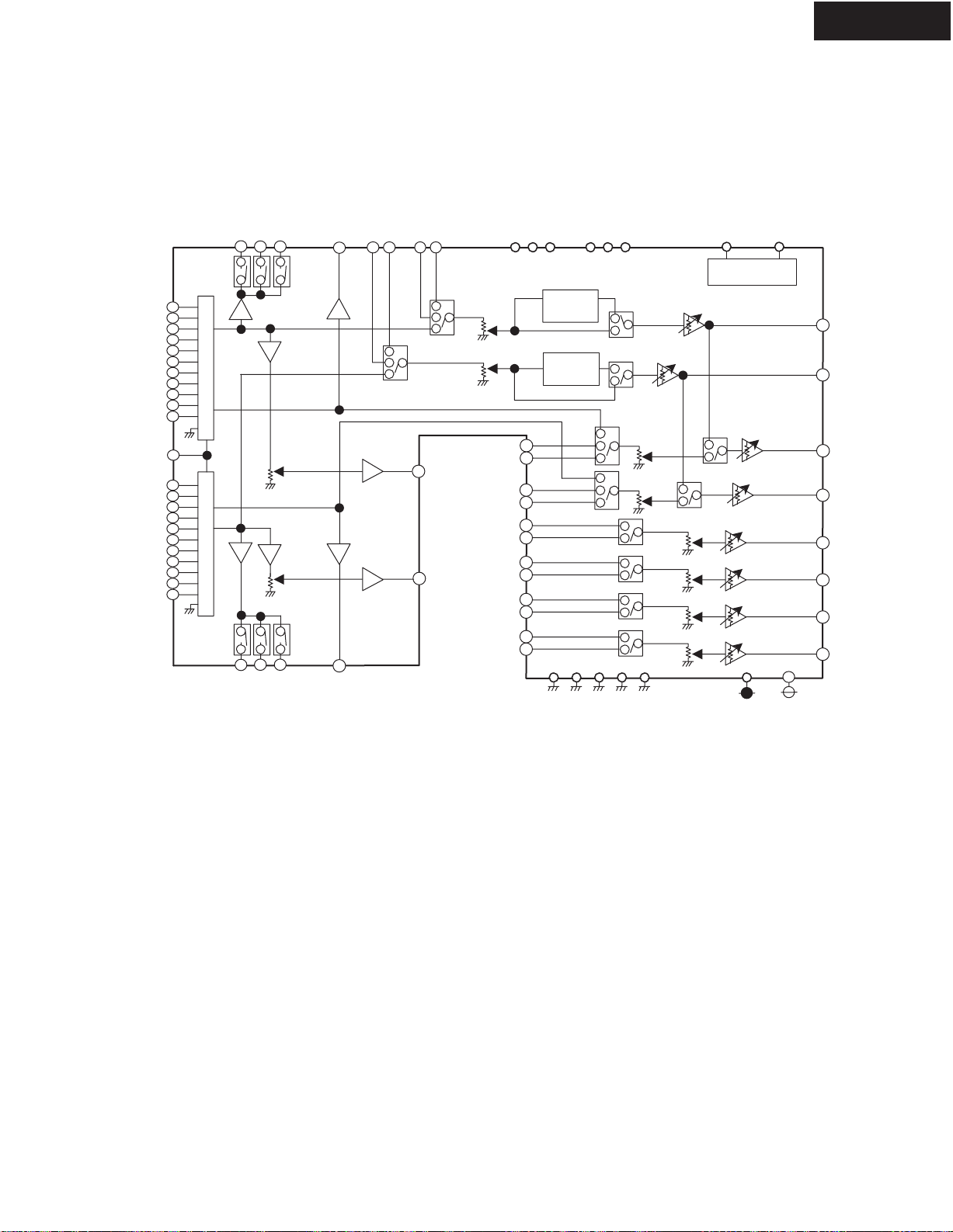
TX-SR506
IC BLOCK DIAGRAMS AND TERMINAL DESCRIPTIONS-15
Q5501 : R2S15211FP (8 ch Electronic Volume and 11 Input Selector and Tone Control)-1/3
SYSTEM BLOCK DIAGRAM
Multi
REC
SUB
Rin
Multi
Lin
Rch Tone
Lch Tone
CLOCK DATA
Lch
mono
Rch
10
11
10
11
Tone
1
2
3
4
5
6
7
8
9
1
2
3
4
5
6
7
8
9
Input selector
Input selector
REC
Input
ATT
Input
ATT
SUB
Out L
for
ADC
Out R
for
ADC
Volume
Volume
Multi
SBLin
Multi
SBRin
Multi
Cin
Multi
SWin
Multi
SLin
Multi
SRin
Bass &
Treble
Bass &
Treble
AGND
Volume
Volume
Volume
Volume
MCU I/F
Volume
Volume
Volume
Volume
Volume
Volume
AVEE
Lout
Rout
SBLout
SBRout
Cout
SWout
SLout
SRout
AVCC
Page 45

TX-SR506
IC BLOCK DIAGRAMS AND TERMINAL DESCRIPTIONS-16
Q5501 : R2S15211FP (8 ch Electronic Volume and 11 Input Selector and Tone Control)-2/3
BLOCK DIAGRAM AND PIN CONFIGURATION
SUBR
SUBL
DGND
DATA
CLOCK
AVEE
INR1
INL1
INR2
INL2
INR3
INL3
INR4
41
42
43
44
45
46
47
48
49
50
51
I/F
MCU
MONO
40
MAIN
39
38
SUB
ADCR
37
ADCL
36
ATT
FLIN2
FRIN2
34 33
35
0/-6/-12/-18dB
SLIN2
SRIN2
32
0~-95dB, -14~+14dB
(1dBstep) (2dB step)
SWIN2
30
31
Bass / Treble
0~-95dB
(1dBstep)
CIN2
29
SBRIN2
28
Tone
-14~+14dB
(2dB step)
+16~-95dB
(1dBstep)
SBLIN2
TRER
27
Tone
Bass / Treble
+16~0dB
(1dBstep)
BASSR2
26
+16~0dB
(1dBstep)
BASSR1
25
AVCC
24
AVCC
23
TREL
22
BASSL2
21
BASSL1
FRC
20
FROUT
19
AGND
18
FLOUT
17
16
FLC
15
6-C
6-OUT (SR OUT)
14
INL4
INR5
INL5
INR6
INL6
INR7
INL7
INR8
INL8
INRA/RECR1
INLA/RECL1
INR9
INL9
52
53
54
55
56
57
58
59
60
61
62
63
64
65 66
REC
67
68
69 70 71
72
74 75 76
73
+16~-95dB
(1dBstep)
+16~-95dB
(1dBstep)
+16~-95dB
(1dBstep)
+16~-95dB
(1dBstep)
+16~-95dB
(1dBstep)
77
78 79
80
AGND
13
5-OUT (SL OUT)
12
5-C
11
4-C
10
4-OUT (SW OUT)
9
AGND
8
3-OUT (C OUT)
7
3-C
6
2-C
5
2-OUT (SBR OUT)
4
AGND
3
1-OUT (SBL OUT)
2
1-C
1
INLB/RECL2
INRB/RECR2
INR10/RECR4
INL10/RECL4
INL11/RECL5
INR11/RECR5
RECL3
RECR3
FLIN1
FRIN1
CIN1
SWIN1
SLIN1
SRIN1
SBLIN1
SBRIN1
Page 46

TX-SR506
IC BLOCK DIAGRAMS AND TERMINAL DESCRIPTIONS-17
Q5501 : R2S15211FP (8 ch Electronic Volume and 11 Input Selector and Tone Control)-3/3
TERMINAL DESCRIPTION
PIN No. Name Function
19,17,
14,12,
9,7,
4,2
20,16,
15,11,
10,6,
5,1
3,8,
13,18
23,27
21,22,
25,26
24
35,34,
33,32,
31,30,
29,28
73,74,
75,76,
77,78,
79,80
FROUT,FLOUT,
6-OUT,5-OUT,
4-OUT, 3-OUT,
2-OUT,1-OUT
FRC,FLC,
6-C,5-C,
4-C,3-C,
2-C,1-C
AGND
TREL, TRER
BASSL1, BASSL2
BASSR1, BASSR2
AVCC
FRIN2, FLIN2,
SRN2,SLIN2,
SWIN2,CIN2,
SBRIN2,SBLIN2
FLIN1, FRIN1,
CIN1,SWIN1,
SLIN1,SRIN1,
SBLIN1,SBRIN1
Output pin of FL/FR/C/SW/SL/SR/SBL/SBR channel
Connects capacitor for reducing click noise of
L/R/C/SW/SL/SR/SBL/SBR channel volume
Analog ground of internal circuit
Frequency characteristic setting pin of L/R channel tone control(Treble)
Frequency characteristic setting pin of L/R channel tone control(Bass)
Positive power supply to internal circuit
Input pin of L/R/C/SW/SL/SR/SBL/SBR channel (Multi IN 1/2)
41 DGND
42 DATA
43 CLOCK
44
46,48,50,
52,54,56,
58,60,64
45,47,49,
51,53,55,
57,59,63
40
38,39
36,37 ADCL, ADCR
72
71 RECR3
61,62,
65,66,
67,68,
69,70
AVEE
INL1, INL2, INL3,
INL4, INL5, INL6,
INL7, INL8, INL9
INR1, INR2, INR3,
INR4, INR5, INR6,
INR7, INR8, INR9
MONO
SUBL,SUBR
RECL3
INRA/RECR1,INLA/RECL1,
INRB/RECR2,INLB/RECL2,
INR10/RECR4,INL10/RECL4,
INR11/RECR5,INL11/RECL5
Digital ground of internal circuit
Input pin of control data
Input pin of control clock
Negative power supply to internal circuit
Input pin of L/R channel (Input Selector)
Input pin of monaural (Input Selector)
Output pin for L/R channel SUB Output
Output pin for L/R channel ADC
Output pin for L/R channel REC Output
Input pin of L/R channel (Input Selector)/
Output pin for L/R channel REC Output
Page 47

IC BLOCK DIAGRAMS AND TERMINAL DESCRIPTIONS-18
Q7003 : M66005-0001AHP (FL Tube Driver)
BLOCK DIAGRAM
TX-SR506
CS
SCK
SDATA
XIN
XOUT
RESET
Vcc1
Vcc2
Vss
Vp
14
15
16
21
20
13
19
60
22
32
Serial
receive
circuit
Clock
generator
data
timing
clock
Display code RAM
Bank 1 : 8bit x 16
Bank 2 : 8bit x 64
code
write
Code/
command
control
circuit
Display
controller
dot data
write
code
select
CG ROM
(35bit x 160)
CG RAM
(35bit x 16)
scan pulse
SEG00
59
33
Segment
output
circuit
Segment/
Digit
select/
output
circuit
Digit
output
circuit
2
SEG26
31
SEG27
24
SEG34
SEG35
23
64
DIG12/SEG36
63
DIG13/SEG37
62
DIG14/SEG38
61
DIG15/SEG39
12
DIG00
1
DIG11
P0
18
P1
17
TERMINAL DESCRIPTION
SYMBOL PIN NAME DESCRIPTIONPIN NO.
13
14
15
16
21,
20
1~12
61~64
23~31
33~59
17, 18
19
60
22
32
RESET Reset input This pin is used to initialize the internal state of the M66004.
CS Chip select input
SCK Shift clock input At the rising edge from "L" to "H", input data is shifted.
SDATA Serial data input Character code or command data to display is input from MSB.
XIN,
XOUT
DIG00 ~
DIG15
SEG00 ~
SEG39
P0, P1 Output port (static operation)
VCC1
VCC2
VSS GND
VP Negative power supply for VFD drive.
Clock input
Clock output
Digit output
Segment output
---
---
---
---
---
"L" : Communication with the MCU is possible.
"H" : Any instruction from the MCU is neglected.
This pin is used to connect a resister and a capacitor externally to
set oscillation frequency.
These pins are used to connect to digit pins of VFD.
These pins are used to connect to segment pins of VFD.
Positive power supply for internal logic.
Positive power supply for high-pressure-resistant output port.
Page 48

IC BLOCK DIAGRAMS AND TERMINAL DESCRIPTIONS-19
Q8001 : TMDS341APFCR (HDMI Switch)-1/2
BLOCK DIAGRAM
A24
B24
A23
B23
A22
B22
A21
B21
VCC (3.3 V)
R
INT
Rx
EQ
V
CC
R
INT
Rx
EQ
V
CC
R
INT
Rx w/
EQ
V
CC
R
INT
Rx w/
EQ
B11
A11
R
EQ
Rx w/
INT
w/
w/
B12
EQ
A12
Rx w/
R
INT
B13
EQ
A13
Rx w/
R
INT
B14
EQ
A14
Rx w/
R
INT
V
CC
(3.3 V)
3-to-1 MUX
TMDS
Drive
TMDS
Drive
TMDS
Drive
TX-SR506
PRE
VSADJ
Y4
Z4
Y3
Z3
Y2
Z2
A34
B34
A33
B33
A32
B32
A31
B31
HPD1
HPD2
HPD3
SCL1
SDA1
VCC (3.3 V)
R
INT
Rx w/
EQ
V
CC
R
INT
Rx w/
EQ
V
CC
R
INT
Rx w/
EQ
V
CC
R
INT
Rx w/
EQ
Control Logic
TMDS
Drive
Y1
Z1
OE
S1
S2
S3
HPD_SINK
SCL_SINK
SDA_SINK
SCL2
SDA2
SCL3
SDA3
Page 49

IC BLOCK DIAGRAMS AND TERMINAL DESCRIPTIONS-20
Q8001 : TMDS341APFCR (HDMI Switch)-2/2
TX-SR506
PIN LAYOUT
VCC
HPD2
SDA2
SCL2
GND
GND
B21
A21
VCC
B22
A22
GND
B23
A23
VCC
B24
A24
GND
VCC
HPD1
TERMINAL DESCRIPTION
PIN NO.
A11, A12, A13, A14
A21, A22, A23, A24
A31, A32, A33, A34
B11, B12, B13, B14
B21, B22, B23, B24
B31, B32, B33, B34
GND
HPD1
HPD2
HPD3
HPD_SINK
NC
OE
PRE
SCL1
SCL2
SCL3
SCL_SINK
SDA1
SDA2
SDA3
SDA_SINK
S1, S2, S3
VCC
VSADJ
Y1, Y2, Y3, Y4
Z1, Z2, Z3, Z4
6, 9, 12, 15
68, 71, 74, 77
49, 52, 55, 58
5, 8, 11, 14
67, 70, 73, 76
48, 51, 54, 57
4, 10, 16, 24, 30, 36, 37, 47,
53, 59, 65, 66, 72, 78
80
62
44
40
1, 20, 41,60
42
19
3
64
46
38
2
63
45
39
21, 22, 23
7, 13, 17 27, 33, 43, 50,
56, 61, 69, 75, 79
18
34, 31, 28, 25
35, 32, 29, 26
NC
GND
A34
B34
VCC
A33
B33
GND
A32
B32
VCC
A31
B31
60595857565554535251504948474645444342
61
62
63
64
65
66
67
68
69
70
71
72
73
74
75
76
77
78
79
80
123456789
NC
SCL1
SDA1
GND
B11
(TOP VIEW)
A11
B12
A12
VCC
I/OPIN NAME
I
I
I
I
I
I
---
O
O
O
I
1011121314151617181920
B13
A13
VCC
GND
DESCRIPTION
Port 1 TMDS positive inputs
Port 2 TMDS positive inputs
Port 3 TMDS positive inputs
Port 1 TMDS negative inputs
Port 2 TMDS negative inputs
Port 3 TMDS negative inputs
Ground
Port 1 hot plug detector output
Port 2 hot plug detector output
Port 3 hot plug detector output
Sink side hot plug detector input
High: 5-V power signal asserted from source to sink and EDID is ready
Low: No 5-V power signal asserted from source to sink, or EDID is not ready
---
No connect
I
Output enable, active low
I
Output de-emphasis adjustment
High: 3 dB Low: 0 dB
I/O
Port 1 DDC bus clock line
I/O
Port 2 DDC bus clock line
I/O
Port 3 DDC bus clock line
I/O
Sink side DDC bus clock line
I/O
Port 1 DDC bus data line
I/O
Port 2 DDC bus data line
I/O
Port 3 DDC bus data line
I/O
Sink side DDC bus data line
I
Source selector input
---
Power supply
I
TMDS compliant voltage swing control
O
TMDS positive outputs
O
TMDS negative outputs
GND
B14
SCL3
A14
SDA3
GND
HPD3
VCC
VCCOENC
PRE
VSADJ
41
40
HPD_SINK
39
SDA_SINK
38
SCL_SINK
37
GND
36
GND
35
Z1
34
Y1
33
VCC
32
Z2
31
Y2
30
GND
29
Z3
28
Y3
27
VCC
26
Z4
25
Y4
24
GND
23
S3
22
S2
21
S1
NC
Page 50

MICROPROCESSOR TERMINAL DESCRIPTIONS-1
Q701 : M30624MHP-456FP (Main Microprocessor)
HT-R560
Pin No. Pin Name I/O Description
1
HDMISEL3
2
HDMISEL2
3
ROMCLK
4
FANCTRL
5
VDSWS2
6
XMLNK
7
XMANT
8
BYTE
9
CNVSS
10
RDSDATA/XMSRSEL
11
SBZ2MUT
12
RESET
13
XOUT
14
VSS
15
XIN
16
VCC1
17
NU
18
POFF
19
DCKDET
RDSCLK/ XMDACRST
20
VDSWS4
21
Z2LPMUT
22
DIRINT0
23
DSPINT1
24
VDSWS6
25
DSPINT0
26
DSPINT2
27
VDSWS3
28
DCKRXD
29
DCKTXD
30
FTXD
31
FRXD
32
FCLK
33
FBUSY
34
XMSRTXD
35
XMSRRXD
36
XMRST
37
DIRCS
38
DIRRST
39
DSPCS
40
FEPM
41
DSPRST
42
DIGCLK
43
DIGSDI
44
DIGSDO
45
FCE
46
AMUT
47
SPRLB
48
SPRLSB
49
SPRLCS
50
I/O
---
---
---
---
---
---
---
---
Act.
O
O
O
O
O
O
O
O
O
O
O
O
O
O
O
O
O
O
O
O
O
O
O
O
O
O
H
HDMI switch IC (TMDS341A) control.
H
HDMI switch IC (TMDS341A) control.
CLK
I
I
I
I
I
I
I
I
I
I
I
CLK
I
I
CLK
I
I
EEPROM IC (R1EX25064) clock output.
L
MWT type : Cooling fan control. Other type : Not used.
L
Video switch IC (AN15880A) control.
---
Not used.
---
Not used.
---
Not used.
---
Processor mode select.
H
MPP type : RDS data input. MDD, MDC type : XM/SIRIUS select.
H
Surround back / Zone 2 muting control.
L
Reset input.
---
Connected to oscillator.
---
Ground.
---
Connected to oscillator.
---
Power supply.
---
Not used.
L
Power failure detection input.
L
Dock detection input.
L
MPP type : RDS clock input. Other type : Not used.
L
Video switch IC (AN15880A) control.
H
Zone 2 line/ preout muting control.
H
DIR/ CODEC IC (CS42518) unlock detection input.
L
DSP IC (D788E001) detection input. (DEC)
L
Video switch IC (AN15880A) control.
L
DSP IC (D788E001) detection input. (NIC)
L
DSP IC (D788E001) detection input. (BUSY)
L
Video switch IC (AN15880A) control.
H
Dock UART data receive signal output.
H
Dock UART data transmitter signal input.
H
Flash microprocessor writing port.
H
Flash microprocessor writing port.
Flash microprocessor writing port.
H
Flash microprocessor writing port.
H
SIRIUS UART data output.
H
SIRIUS UART data input.
---
Not used.
L
DIR/ CODEC IC (CS42518) chip select output.
L
DIR/ CODEC IC (CS42518) reset control output.
L
DSP IC (D788E001) chip select output.
H
Flash microprocessor writing port.
L
DSP IC (D788E001) reset control output.
DIR IC (CS42518) clock output.
H
DIR IC (CS42518) data input.
H
DIR IC (CS42518) data output.
H
Flash microprocessor writing port.
H
Audio muting control output.
H
Speaker B relay control output.
H
Surround back speaker relay control output.
H
Center/ Surround speaker relay control output.
Page 51

MICROPROCESSOR TERMINAL DESCRIPTIONS-2
Q701 : M30624MHP-456FP (Main Microprocessor)
HT-R560
Pin No. Pin Name I/O Description
51
SPRLF
52
ROMSDO
53
VOLDAT
54
VOLCLK
55
ROMSDI
56
VPOWER
57
APOWER
58
POFF2
59
NU
60
VDSWS1
61
VDSWS7
62
VCC2
63
SEC1H
64
VSS
65
PROTECT
66
VOLH
67
THERMAL
68
INIT3
69
INIT2
70
INIT1
71
BAND
72
SYSOUT
73
SYSIN
74
VDSWS8
75
REMIN
76
STEREO
77
SD
78
HPDET
79
VOLB
80
VOLA
81
ROMCS
82
MICDET
83
MICMUT
84
LEDSTBY
85
FLDSDO
86
FLDCLK
87
FLDCS
88
FLDRST
89
PLLSCL
90
91
92
93
94
95
96
97
98
99
100
PLLSDA
KEYINT1
KEYINT0
KEY3
KEY2
KEY1
AV S S
KEY0
VREF
AV C C
HDMISEL1
I/O
---
---
---
---
---
---
Act.
O
O
O
O
O
O
O
O
O
O
O
O
O
O
O
O
O
O
O
O
H
Front Speaker relay control output.
H
EEPROM IC (R1EX25064) data transmitter output.
H
Volume/ selector IC (R2S15211) data output.
CLK
I
I
I
I
I
I
I
I
I
I
I
I
I
I
I
I
I
CLK
CLK
I
I
I
I
I
I
Volume/ selector IC (R2S15211) clock output.
H
EEPROM IC (R1EX25064) data input.
H
Video circuit power supply control.
H
Main power supply control.
L
Power failure detection 2.
---
Not used.
L
Video switch IC (AN15880A) control.
L
Video switch IC (AN15880A) control.
---
Power supply.
H
Secondary-1 (high) power supply control.
---
Ground.
H
Speaker protect detection.
A/D
Power amplifier output voltage detection.
A/D
Thermal detection.
A/D
Initial setting.
A/D
Initial setting.
A/D
Initial setting.
A/D
Initial setting.
L
RI (System control) output.
H
RI (System control) input.
L
Video switch IC (AN15880A) control.
L
Remote control signal input.
L
FM stereo detection.
L
FM/ AM receive detection.
H
Headphone detection input.
H
Rotary encoder (volume) input.
H
Rotary encoder (volume) input.
L
EEPROM IC (R1EX25064) chip select output.
L
Setup Mic detection input.
H
Setup Mic muting output.
H
Standby LED control output.
H
FL driver IC (M66005) data output.
FL driver IC (M66005) clock output.
L
FL driver IC (M66005) chip select output.
L
FL driver IC (M66005) reset output.
Tuner unit I2C clock output.
H
Tuner unit I2C data input/ output.
L
Key input.
L
Key input.
A/D
Key input.
A/D
Key input.
A/D
Key input.
---
Ground. (A/D)
A/D
Key input.
---
Power supply. (A/D reference)
---
Power supply. (A/D)
H
HDMI switch IC (TMDS341A) control.
Page 52

SERVICE PROCEDURE-1
1. Replacing the fuses
This symbol located near the fuse indicates that the
fuse used is show operating type, For continued protection against
fire hazard, replace with same type fuse, For fuse rating, refer to
the marking adjacent to the symbol.
Ce symbole indique que le fusible utilise est e lent.
Pour une protection permanente, n'utiliser que des fusibles de meme
type. Ce demier est indique la qu le present symbol est apposre.
REF NO. PART NAME DESCRIPTION PART NO. REMARKS
F901
F901 or
F901
F901 or
F6901
F6901 or
F6902
F6902 or
FUSE
FUSE
FUSE
FUSE
FUSE
FUSE
FUSE
FUSE
8A-UL/T-233
8A-T/UL-ST2
4A-SE-EAK FUSE
4A-SE-TL250V
10A-UL/T-233
10A-T/UL-ST2
10A-UL/T-233
10A-T/UL-ST2
252329GR
252261GR
252077GR
252277GR
252330GR
252333GR
252330GR
252333GR
HT-R560
!, <MDD, MDC>
!, <MDD, MDC>
!, <MPP>
!, <MPP>
!
!
!
!
<Notes>
<MDD> : USA model
<MDC> : Canadian model
<MPP> : European model
2. Safety check out
(U.S.A. model only)
After correcting the original service problem, perform the following safety check before releasing the unit to the customer.
Leakage current Check
Measure the leakage current to a known earth ground (water pipe or conduct etc.) by connecting a leakage current
tester between the earth ground and exposed metal parts of the unit (input/output ground terminals, screw heads or metal overlays etc.).
Plug the power supply cord directly into a 120Vac 60Hz wall socket and turn ON/STANDBY button on.
Any current measured must not exceed 0.5mA.
3. Memory Backup
This model uses a EE-PROM IC in order to retain radio presets and other settings. So, memory contents will be
kept eternally with no care.
4. To initialize the unit
1. Press and hold down VCR/DVR button, then press ON/STANDBY button when the unit is powered on.
2. After " Clear " is displayed, the preset memory and each mode stored in the memory, are initialized and
will return to the factory settings.
Page 53

SERVICE PROCEDURE-2
5. To check version of Main microprocessor and DSP
1. Press and hold down DISPLAY button, then press ON/STANDBY button when the unit is power on.
The main microprocessor version will be displayed on Front Display for about 3 seconds.
Ex.
Ver.1.02/08408A
2. Press + (TONE) button while the version is displayed. Then, " DSPSR506:08130A " will be displayed.
In this way, as + (TONE) button is pressed while a version is displayed, the next information will be displayed.
If - (TONE) button is pressed, the order will be reversed.
HT-R560
Version of Main microprocessor (Q701)
Version of DSP (Q282)
- (TONE)
Ver.1.02/08408A
+ (TONE)
DSPSR506:08130A
3. Press ON/STANDBY button to power off.
6. Replacing Power Amplifier Parts
When a power amplifier of certain channel is broken and goes into Protect mode, the following parts in the channel
must be replaced at the sametime, because these parts get damage in most cases.
L ch
Q6001, 6011
Q6031, 6041
Q6051, 6061
C5051, 6041
R6021, 6071
R6081, 6091
R6101
R ch
Q6002, 6012
Q6032, 6042
Q6052, 6062
C5052, 6042
R6022, 6072
R6082, 6092
R6102
Center
Q6000, 6010
Q6030, 6040
Q6050, 6060
C5050, 6040
R6020, 6070
R6080, 6090
R6100
Q6003, 6013
Q6033, 6043
Q6053, 6063
C5053, 6043
R6023, 6073
R6083, 6093
R6103
Refer to “SCHEMATIC DIAGRAMS-2 (POWER AMPLIFIER SECTION)”
R5001
C5001
C5011
+
<Ex.> Front Lch
R5091
R5021
R5011
R5041
+
C5021
D5001
R5101
R5111
Q5001
R5051
-0.65V
R5061
R5071
Q5051
R5081
Q5011
+
C5041
C5101
C5111
R5181
+1.1V
R5161
Q5031
+
R5031
C5081
0V
R5231
R5171
C5091
Q5041
R5191
+
-1.1V
R5201
R5131
+1.0V
R6031
R6001R6011
-0.3V
IDLING
ADJ.
R6041
-0.4V
R6051
L ch
Q6001
Q6011
R6021
+
Surround Surrond BackFront
+0.6V
C5051
-0.6V
Q6004, 6014
Q6034, 6044
Q6054, 6064
C5054, 6044
R6024, 6074
R6084, 6094
R6104
Q6031
R6081
+
C6041
R6071
Q6041
R ch
IDLING
CHECK
P6081
ID+
ID-
R6091
Q6051
R6141
R6101
Q6061
R6171
D6001
L ch
Q6005, 6015
Q6035, 6045
Q6055, 6065
C5055, 6045
R6025, 6075
R6085, 6095
R6105
R6161
Q6071
C6051
R6151
R6191
D6011
VPRO
R6181
VOLH
IPRO
SPL
R ch
Q6006, 6016
Q6036, 6046
Q6056, 6066
C5056, 6046
R6026, 6076
R6086, 6096
R6106
Page 54

OPERATION CHECK-1
DISPLAY
ON/STANDBY
TONE
SPEAKER PROTECT-1
Circuit configuration
The unit go into protect mode when either of thermal detection, dc voltage detection or current detection circuit operates.
Power amplifier
FL
FR
C
SL
SR
SBL
SBR
Q6071
Q6072
Q6070
Q6073
Q6074
Q6075
Q6076
Condition to operate
The unit will go into the Protect mode under the following conditions.
1. Thermal condition
T ( C) Thermal sensor temperature
100 <
-30 >
150 <
90 < (40 C when power on)
90 < (The unit powered on longer than 24 hours)
2. DC voltage condition
The sum of dc voltage of 7 channel speaker outputs is more than 7 V.
VPRO : DC voltage detection
IPRO : Current detection
Thermal sensor
Q6380
+B
IPRO
VPRO
Q6703
Q6702 Q6701
--->
--->
--->
--->
--->
THERMAL
PROTECT
Protect
On (after 10 min.)
On (immediately)
On (immediately)
On (immediately)
On (immediately)
67
Q701
Main Microprocessor
65
67
APOWER
RL901
Power trans
Q9002
TX-SR506
AC in
3. Current condition
The ac current of speaker outputs is more than 35 A.
This condition is equivalent to TEST-4-35 in OPERATION CHECK-3.
Thermal detection check
[When]
Exchange thermal sensor PC board ass'y (NAETC-9421).
[Procedure]
1. Press and hold down DISPLAY
button, then press ON/STANDBY
button when the unit is powered on.
The microprocessor version will be displayed for 3 seconds.
FL Display
<Ex.>
2. Press TONE
VOLH (V)
Voltage of VOLH port
button while the version is displayed.
<Ex.>
Ver.1.02/08408A
000 033 F:x S:H
T ( C)
Thermal sensor temperatuer
State of cooling fan
x : Stop
L : Low speed
H : High speed
3. Confirm that the displayed temperature is within +/-20 C from the ambient temperature.
4. Press ON/STANDBY button.
Turn off
Clear
Power supply voltage of +/-B1
H : VH (high voltage)
L : VL (low voltage)
Page 55

OPERATION CHECK-2
SPEAKER PROTECT-2
DC Voltage detection check
[When]
1. Exchange power transistors (Q6050 - Q6056, Q6060 - Q6066).
2. Exchange amplifier PC board ass'y (NAAF-9419).
[Procedure]
Note : No load. No input.
1. Press and hold down CD button, then press ON/STANDBY button while the unit is powered on.
" Test - _ " is displayed only for 5 seconds.
FL Display
2. Press AUX button while the characters of " Test - _ " are displayed.
The unit will be in the state of " Test-4-00 ".
3. Repeatedly press + (TONE) button until the characters of " Test-4-21 " are displayed.
Test - _
Test - 4-00
Test - 4-21
Blinks
TX-SR506
Check whether the operation starts and continues automatically as follows.
Test - 4-21
Front L ch
Protect OK
Check
Test - 4-22
Front R ch
Protect OK
Check
Test - 4-23
Center ch
Protect OK
Test - 4-24
Check
Surround L ch
Check
Protect OK
If all channels are OK, the characters of " Test-4-35 " are displayed.
Test - 4-25
Protect OK
Test - 4-26
Protect OK
Test - 4-27
Protect OK
Protect
Surround R ch
Check
Surround Back L ch
Check
Surround Back R ch
Check
Test - 4-35
4. Press ON/STANDBY button.
Turn off
Clear
Page 56

OPERATION CHECK-3
SPEAKER PROTECT-3
Current detection check
[When]
1. Exchange power transistors (Q6050 - Q6056, Q6060 - Q6066).
2. Exchange amplifier PC board ass'y (NAAF-9419).
[Procedure]
Notes : No input.
Do not check two or more channels at the same time.
Do not connect a dummy load to speaker terminal longer than 2 seconds.
1. Press and hold down CD button, then press ON/STANDBY button while the unit is powered on.
" Test - _ " is displayed only for 5 seconds.
FL Display
2. Press AUX button, while " Test - _ " is displayed.
The unit will be in the state of " Test-4-00 ".
3. Repeatedly press + (TONE) button until " Test-4-35 " is displayed.
The shape of wave form of <Fig-1> is output from the speaker terminal in this state.
Test - _
Test - 4-00
Blinks
TX-SR506
Test - 4-35
4. Connect the dummy load of 3 ohms to the Front L ch speaker terminals.
At this time, confirm that the speaker relay is not turned off.
Test - 4-35
5. Connect the dummy load of 1 ohm to the Front L ch speaker terminals.
At this time, confirm that the speaker relay is turned off and " Protect " is displayed.
Protect
Disconnect the dummy load immediately after checking the display of " Protect ".
Test - 4-35
6. Check other channels according to the same procedure as 4 and 5.
7. Press the ON/STANDBY button.
Turn off
Clear
<Fig-1>
Test wave form
2 mS 2 mS
20 mS
Page 57

OPERATION CHECK-4
POWER SUPPLY CONTROL
Configuration
The power supply voltage of +/-B1 for power amplifier is changed by the relays (RL6901, 6902).
Power amplifier
FL
FR
C
SL
SBR
SR
SBL
Condition to operate
The power supply voltage of +/-B1 under the following condition.
The state of "VOLH", "T", and "VH or VL" can be confirmed on the FL display. Refer to “OPERATION CHECK-1”.
Operation of power supply control (VH or VL)
T ( C)
Thermal sensor
temperature
< 60
60 <
Output sensor
Thermal sensor
Q6380
THERMAL
VOLH
VOLH (V)
< 0.33
VH
VL VL
67
(Main Microprocessor)
66
VOLH port of MPU
0.33 to 1.65
5 min.
VL
Q701
MPU
63
1.65 <
5 sec.
VL
VL
To Power trans.
SEC1H
Operation of relay
VH : high voltage
VL : low voltage
S1H+
S1H-
S1L+
S1L-
Q6707
RL6901
RL6902
+22V
D6901
D6903
RL6901, 6902
ON
Off
+B1
++
-B1
TX-SR506
To Power amp.
section
Output sensor
[When]
Same as the Current detection check on "OPERATION CHECK-3".
[Procedure]
Notes : No output. No input.
1. Press and hold down CD button, then press ON/STANDBY button while the unit is powered on.
" Test - _ " is displayed only for 5 seconds.
Test - _
Blinks
2. Press AUX button while " Test - _ " is displayed. The unit will be in the state of " Test-4-00 ".
Test - 4-00
3. Repeatedly press + (TONE) button until " Test-4-36 " is displayed.
Test - 4-36
4. At this time, confirm that the red characters of " FM STEREO " is displayed.
And, confirm that the relays RL6901 and RL6902 are turned off in 2 or 3 seconds.
Test - 4-36
5. Press + (TONE) button then " Test-4-37 " will be displayed.
Test - 4-37
6. At this time confirm that the red characters of " FM STEREO " is displayed.
And, confirm that the relays RL6901 and RL6902 are turned off in 2 or 3 seconds.
Test - 4-37
Test - 4 - 36 : Front L, R, Center, Surround L ch check
FM STEREO
Test - 4 - 37 : Surround L, R, Surround back L, R ch check
FM STEREO
7. Press ON/STANDBY button.
Turn off
Clear
Thermal sensor
Same as the Thermal detection in "OPERATION CHECK-1".
Page 58

OPERATION CHECK-5
COOLING FAN
Note : MWT, MWO, MWF type only
Circuit configuration
TX-SR506
Power amplifier
FL
FR
C
SL
SBR
SR
SBL
Output sensor
Thermal sensor
Q6380
THERMAL
VOLH
67
Q701
Main Microprocessor
66
FANCTRL
63
Condition to operate
The cooling fan will stop or rotate at high speed or low speed under the following condition.
Operation of Cooling Fan
VOLH port of MPU
0.35 to 1.75
High Speed
1.75 to 3.3V
High Speed
High Speed
T ( C)
Thermal sensor
temperature
55 to 110
-30 to 55
VOLH (V)
0 to 0.35
High Speed
Stop Low Speed
Fan drive
Q9101, 9102
Q9111, 9112
Cooling fan
Page 59

DEBUG MODE-1
DISPLAY
ON/STANDBY
DISPLAY
DSP dubug mode
DSP DEBUG MODE-1
The operations of DSP and DIR etc are able to checked by the information displayed on FL in this debug mode.
This information will help to analysing digital audio no sound trouble.
To set in Debug mode
1. Press and hold down DISPLAY
The version number of microprocessor is displayed only for 3 seconds.
button, then press ON/STANDBY
button while the unit is powered ON.
TX-SR506
Ver.1.02/08408A
2. Press + (TONE) button within 3 seconds above, the version number of DSP will be displayed for 5 seconds.
DSPSR506:08130A
3. Press DISPLAY
To exit
Press ON/STANDBY button.
button while the DSP version is displayed. The status of DSP and DIR etc will be displayed.
<Ex.>
E1A48K0N/OFFPoO
Version of Main Microprocessor FW
*Number depends on the version.
Version of DSP FW
*Number depends on the version.
DSP dubug mode
Content of Display
FL Display
2
1
1
DIR Input Lock/ Unlock
E = UNLOCK
= LOCK
DIR Input RX
2
0 = None
1 = COAXIAL 1
2 = COAXIAL 2
3 = COAXIAL 3
4 = OPTICAL 1
5 = OPTICAL 2
6 = OPTICAL 3
7 = HDMI 1
8 = HDMI 2
9 = HDMI 3
A = HDMI 4
B = HDMI 5
C = HDMI 6
D = FRONT
4
56 8
71039
4
Sampling Frequency, Emphasis
32K = 32 kHz without Emphasis
44K = 44.1 kHz without Emphasis
48K = 48kHz without Emphasis
64K = 64 kHz
88K = 88.2 kHz
96K = 96 kHz
176 = 176.4 kHz
192 = 192 kHz
32e = 32 kHz with Emphasis
44e = 44.1 kHz with Emphasis
48e = 48 kHz with Emphasis
CODEC Clock Mode
5
N = Normal
U = Up Sampling
H = High Sampling (Double Rate)
D = Down Sampling
Q = Quad Rate
11
3
DIR/ ADC Fix Mode
D = Digital(SPDIF)
A = Analog
M = Analog Multich
p = PCM Fixed
d = DTS Fixed
6
DIR Detect Type
0 = Analog
1 = PCM
2 = Not PCM
3 = Data
4 = DTS CD (Not used)
5 = Multich
6 = Not Decided
Page 60

DEBUG MODE-2
DSP DEBUG MODE-2
Content of Display (Continued)
7
DSP Port
This figure is displayed in hexadecimal form.
If this is transformed to binary form, each bit indicates
the following DSP port status. Refeo to
bit 0 = NIC
bit 1 = DEC
bit 2 = BUSY
bit 3 = Exec Wait
8
DSP Sequence
00 - FE = Boot
2D = Mute control
FF = Free
9
DSP Detect Format
P = PCM (Analog)
D = Dolby Digital
d = DTS
A = AAC
S = DSD
p = Dolby Digital+
T = True HD
H = DTSHD High Resolution
M = DTSHD Master Audio
? = Unknown
(Normal state)
(Abnormal state)
<Fig-1>
TX-SR506
DSP Decode
10
o = Decode OK
x = Decode NG
.
11
Mute output device
This figure are displayed in hexadecimal form.
If these are transformed to binary form, each bit indicates
the IC which outputs error and mute. Refeo to
bit 0 = Selector IC (Q5501)
bit 1 = Effector
bit 2 = DSP (Q201)
bit 3 = DIR (Q301)
<Fig-1>
Hexadecimal
Translation
Binary
0 = 0 0 0 0
1 = 0 0 0 1
2 = 0 0 1 0
4 = 0 1 0 0
8 = 1 0 0 0
bit 0
bit 1
bit 2
bit 3
<Fig-1>
.
Trouble Shooting by DSP DEBUG MODE
1. This debug mode will be useful in digital audio no sound or sound drop-out trouble.
2. Check information on FL display, then identify bad parts, and replace or resolder it.
3. Remdies Written below are of typical case. So, more detailed check may need in actual cases.
4. Before replace ICs below, resolder the pins first to save resources.
<Note>
Function
MPU (Main microprocessor)
DSP
DIR and DAC
Flash ROM
SDRAM
Audio processor (Selector/ Volume)
Digit No.
on FL
Symptom on FL display
"E" is displayed
1
Displayed frequency is different
4
from input signal.
Displayed audio format is
6
different from input signal.
Circuit No.
Q701
Q201
Q301
Q282
Q281
Q5501
Cause of trouble
No input signal to DIR.
No input signal to DIR.
No input signal to DIR.
Schematic Diagrams
SD-3
SD-7
SD-3
SD-7
SD-7
SD-1
Remedy
1. Find out which digital input does not work.
2. Confirm where the digital waveform stops
between the digital input and DIR.
3. Resolder pins of the bad part or replace it with
new one.
The same as above.
The same as above.
Page 61

DEBUG MODE-3
03
DSP DEBUG MODE-3
Trouble Shooting by DSP DEBUG MODE (Continued)
Digit No.
on FL
Symptom on FL display
Cause of trouble Remedy
TX-SR506
Continue to display "1"
7
Continue to display "2"
Continue to display "3" to"7"
Continue to display "8" to "F"
Continue to display "03
8
Continue to display "0505"
Continue to display "0909" to "1010"
Continue to display "1919"
Display "2121" to "2323",
then return and signal format
indicator is flashing.
Interface between DSP and MPU is no good.
Connection from DIR to DSP is no good.
Interface between DSP and MPU is no good.
DSP Sequence is no good.
"
Communication between DSP and MPU
is no good.
Writing from MPU to DSP is no good.
DSP program does not run properly.
Flash ROM or SDRAM is no good.
The unit was powered off during DSP
firmware updating.
DSP program does not run properly.
Flash ROM or SDRAM is no good.
The same remedy as 10 -b.
The same remedy as 9 .
The same remedy as 10 -b.
Check 8 items.
1. The same remedy as 10 -b.
2. Check the voltage of the power supply pin
of DSP.
3. Check the reset port and clock input of DSP by
oscilloscope, and find out bad part.
4. Flash ROM firmware is no good. Update.
5. DSP or MPU is broken. Replace MPU.
DSP is impossible to replace, so replace with
a new PC board.
1. Flash ROM firmware is no good, update.
2. Check DSPSDO pin of MPU by oscilloscope.
If no signal, find out bad part connected.
3. Flash ROM or SDRAM is no good, replace.
4. DSP or MPU is broken, replace the same
method as above 5.
1. Flash ROM firmware is no good, update.
2. Flash ROM or SDRAM is broken, replace.
Initialize the unit.
(Press STANDBY/ON button while pushing
VCR/DVR button when the unit is powered on.)
1. Flash ROM firmware is no good, upgrade.
2. Flash ROM or SDRAM is broken, replace.
Continue to display "2424" to
"2727", or "4040" to "4343".
Continue to display "2929" to "3232"
Displayed audio encoding
9
format is different from input
signal.
"x" is displayed.
10
This identifies IC which outputs
11
error.
DSP program does not run properly.
Or audio clock to DSP is no good.
DSP setting is failured.
Input signal to DSP is no good.
a. No input signal to DSP.
b. Interface between DSP and MPU is
no good.
The IC outputs error to MPU.
1. Flash ROM program is no good, upgrade.
2. Flash ROM or SDRAM is broken, replace.
3. Check DSP drive clock freq. by oscilloscope.
If no signal, find out bad part connected.
4. Check audio clock to DSP by oscilloscope.
If no signal, find out bad part connected.
1. Flash ROM firmware is no good, upgrade.
2. Flash ROM or SDRAM is broken, replace.
1. Confirm where the digital waveform stops
between DIR and DSP by oscilloscope.
2. Q202, P8001 may relate.
3. Resolder pins of the bad part or replace it with
new one.
The same as above.
1. Confirm where the digital waveform stops
between MPU and DSP by oscilloscope.
2. P8001, P8002, P8003 may relate.
3. Resolder pins of the bad part or replace it with
new one.
Replace the IC chip.
DSP is impossible to replace, so replace with a
new PC borad.
Page 62

DEBUG MODE-4
DISPL
ON/
ANDBY
SETUP
SETUP
RETURN
SERVICE INFORMATION MODE
Trouble Shooting by Displaying Service information
This service information display system is helpful in analyze the status when the unit goes into Protect mode and is powered off.
Pay attention that the status will change if a button is pushed.
TX-SR506
1. Press and hold down DISPL
The version of main microprocessor is displayed only for 3 seconds.
<Ex.>
2. Press SETUP
Listening Mode Code List
Code Listening Mode
01
02
03
04
07
09
0A
0B
0C
0D
0E
0F
20
21
22
23
24
25
button within 3 seconds above, the following informations are displayed.
<Ex.>
Power off Cause
P : Protect
- : Other
Pure Audio
Direct
Stereo
Mono
Mono Movie
Orchestra
Unplugged
Studio-Mix
TV Logic
All CH Stereo
Full Mono
PLII Movie T-D
PLII Movie
PLII Music
PLII Game
PLIIx Movie
PLIIx Music
PLIIx Game
AY Y button, then press ON/
Ver.1.02/08408A
- 80 F 27 DD
Temperature
: xx F or xx C
Code
26
27
28
40
41
42
43
44
29
30
30
3B
30
30
30
30
STANDBY
Information Displayed
Volume Level
xx
Listening Mode
Neo:6 Cinema
Neo:6 Music
Neural Surround
PLII Movie THX
PLIIx Movie THX
Neo:6 Cinema THX
PLII Movie THX Games
Neo:6 Cinema THX Games
Neural-THX
Dolby Digital
DTS
DTS96/24
AAC
MultiCh
Dolby Digital Plus
Dolby TrueHD
button while the unit is powered ON.
Version of Main microprocessor
*Number depends on the version.
Listenning Mode
xx ---> Refer to the code list below.
Listening Mode
Code
DTS-HD High Resolution
30
DTS-HD Master Audio
30
DSD
30
+PLIIx Movie
39
+PLIIx Music
3A
Dolby EX
38
+Neo:6
37
DTS Matrix
31
DTS Discrete
31
THX Cinema
50
THX Surround EX
58
THX Ultra2 Cinema
5C
THX Music Mode
5D
THX Games
5E
+PLIIx Movie THX
59
+Neo:6 THX
57
+Neural-THX
3D
DTX Matrix THX
51
DTS Discrete THX
52
3. Press SETUP
4. Press RETURN
button again. The following information are displayed.
<Ex.>
button. The information will be cleared.
<Ex.>
01:23 10hour
Time after Power on
xx : xx
ProtectData CLR
Time after Initialize
xx hour
Page 63

ADJUSTMENT PROCEDURE-1
R6041
R6042
R6040
R6043
R6044
R6045
R6046
2.5 mV
1.5 mV
P6081
P6082
P6080
P6083
P6084
P6085
P6086
9 mV
Leave it as it is
11 mV
6 mV
Leave it as it is
8 mV
12 +/- 3
9 +/- 3
IDLING CURRENT ADJUSTMENT
[When]
1. Exchange Power transistor (Q6050 - Q6056, Q6060 - Q6066).
2. Amplifier PC board (NAAF-9419).
[Procedure]
Refer to "ADJUSTMENT PROCEDURE-2 " for the adjustment points and the test points.
<Note> No load and No signal
1. Before idling adjustment, turn the trimming resistors fully to counter clockwise.
2. Connect the dc voltmeter to test points,
using two 100 ohm resistors between the poles of the jig terminal and the dc voltmeter terminals.
100 ohms
DC voltmeter
3. Connect the ac power cord to a wall outlet. And press ON/STANDBY button to turn the power on.
4. Adjust the trimming resistors as the following procedure immediately after power on.
Channel
Front Left
Front Right
Center
Surround Left
Surround Right
Surround Back Left
Surround Back Right
(1/4 watt)
Adjustment point
R6041
R6042
R6040
R6043
R6044
R6045
R6046
Jig terminal
Test point
P6081
P6082
P6080
P6083
P6084
P6085
P6086
Test point
ID+
ID-
Adjustment value
2.5 mV
1.5 mV
HT-R560
5. Wait for 4 - 6 minutes. (Heat running)
6. Re-adjust the trimming resistors as the following procedure.
Channel Measured value Adjustment value
Front Left, Front Right
and Center
Surround Left
Surround Right
Surround Back Left
Surround Back Right
<Notes>
Idling currents are stabilized in about 10 minutes after power on.
In below 9 mV
In case 9 - 11 mV
In case over 11 mV
In case below 6 mV
In case 6 - 8 mV
In case over 8 mV
9 mV
Leave it as it is
11 mV
6 mV
Leave it as it is
8 mV
Specifications
12 +/- 3
9 +/- 3
mV
7. Disconnect the dc voltmeter.
8. Press ON/STANDBY button to turn the power off. And disconnect the ac power cord.
mV
Page 64

ADJUSTMENT PROCEDURE-2
IDLING CURRENT ADJUSTMENT
Adjustment points and the test points
HT-R560
Test pointAdjustment point
(Trimming resistor)
R6046
Amplifier PC board
(NAAF-9414)
Front side
SBR
SR
NCAF-9419
SBL
SL
R6045
R6044
R6043
BIAS
BIAS
BIAS
BIAS
R6046
P6084
P6083
ID+
P6085
ID+
P6086
Surround Back
P6086
ID+
Right ch
R6045
ID-
ID+
P6085
ID-
Surround Back
Left ch
R6044
ID-
Surround
Right ch
R6043
ID-
ID+
P6084
ID+
P6083
ID-
ID-
Surround
Left ch
ID+
ID-
R
BIAS
R6042
P6082
ID-
ID+
R6042
P6082
BIAS
L
R6041
P6081
ID+
ID-
Front Right ch
ID+
ID-
R6041
P6081
R6040
BIAS
ID+
ID-
C
P6080
Front Left ch
ID+
ID-
R6040
P6080
Center ch
ID+
ID-
Page 65

HT-R560
<Note>
Parts marked by "NSP" are generally unavailable because
they are not in our Master Spare Parts List.
NOTE : THE COMPONENTS IDENTIFIED BY THE MARK
! ARE CRITICAL FOR RISK OF FIRE AND
ELECTRIC SHOCK. REPLACE ONLY WITH PART
NUMBER SPECIFIED.
<Notes>
(B) : Black model
(S) : Silver model
<MDD> : USA model
<MDC> : Canadian model
<MPP> : European model
EXPLODED VIEW PARTS LIST
REF. NO. PART NAME DESCRIPTION Q'TY PART NO. (SN) REMARKS
EXPLODED
A001 CHASSIS (FRONT) 1 27100513A
EXPLODED
A002 SCREW 3TTB+8B(3CM)SR 5 801637
EXPLODED
A003 B PLATE --- 1 28133425
EXPLODED
A003 B PLATE --- 1 28133426
EXPLODED
A004 RETAINER (F) 1 27142099
EXPLODED
A005 SCREW 3TTB+8B(3CM)SR 2 801637
EXPLODED
A011 SCREW 2.6TTB+8B(3BC) 18 838426088GR
EXPLODED
A012 SCREW 2.6TTB+8B(3BC) 3 838426088GR
EXPLODED
A013 WIRE TIE BSK-1 8 260208
EXPLODED
A016 SCREW 3TTB+8B(3CM)SR 1 801637
EXPLODED
A018 HOLDER KGLS-22S 3 27190369
EXPLODED
A020 HOLDER KGLS-16RT 2 27190511
EXPLODED
A021 HOLDER KGPS-16RF 5 27190991
EXPLODED
A022 HOLDER KGLS-10RT 1 27190428A
EXPLODED
A030 SCREW 4TTC+8C(3BC) 4 830440089GR
1/69 PAGE
(B)
(S)
Page 66

EXPLODED
A031 SPACER --- 1 27270439
EXPLODED
A033 LABEL (PT) 1 29363379-1
EXPLODED
A035 HOLDER KGLS-14RT 1 27190524
EXPLODED
A037 BUSHING S-RELIEF #2271 1 27300750
EXPLODED
A039 TAPE TAPE(CLOTH-16U) (1) 29110083
EXPLODED
A040 HEAT SINK (AS) 1 27160602A
EXPLODED
A041 BRACKET (HT-L) 1 27131016B
EXPLODED
A042 BRACKET (HT-R) 1 27131017A
EXPLODED
A043 SCREW 3TTB+8B(3CM)SR 4 801637
EXPLODED
A044 SCREW 3TTB+8B(3CM)SR 4 801637
EXPLODED
A046 SCREW 3TTB+8B(3CM)SR 2 801637
EXPLODED
A047 SCREW 3TTB+8B(3CM)SR 2 801637
EXPLODED
A048 SCREW 3TTB+8B(3CM)SR 1 801637
EXPLODED
A049 SCREW 3SMS8W.SW+14B(CU) 14 801634
EXPLODED
A050 IB CUSHION W15 x 3t TAPE 1 28141585
EXPLODED
A052 SCREW 3TTB+8B(3CM)SR 1 801637
EXPLODED
A055 KNOB (VOL) BLACK 1 28326514
EXPLODED
A055 KNOB (VOL) SILVER 1 28326515
EXPLODED
A060 COVER (B) (Bent) 1 28210010
EXPLODED
A060 COVER (S) (Bent) 1 28210011
EXPLODED
A060 COVER (B) (Not bent) 1 28210010Z
EXPLODED
A060 COVER (S) (Not bent) 1 28210011Z
EXPLODED
A061 SCREW 3TTB+8B(3BC) 6 838430088GR
EXPLODED
A061 SCREW 3TTB+8B(3CM)SR 6 801637
EXPLODED
A062 CUSHION --- 2 28141681
EXPLODED
A066 BOTTOM LEG TX-SR506 4 27175441A
EXPLODED
A067 WASHER W3 x 8F(3CM) 4 87613008GR
EXPLODED
A068 SCREW 3TTB+10B(3BC) 4 838430108GR
EXPLODED
A071 CUSHION --- 3 28141688
EXPLODED
A072 CHASSIS 506 1 ---
EXPLODED
A073 F PANEL (B)MDD/H560 1 27213076A
EXPLODED
A073 F PANEL (B)MDD/H560 1 27213076A
EXPLODED
A073 F PANEL (B)MPP/H560 1 27213078A
2/69 PAGE
!
(B)
(S)
(B)
(S)
(B) <MDD, MDC>
(S) <MDC>
(B)
(S)
NSP
(B) <MDD>
(B) <MDC>
(B) <MPP>
Page 67

3/69 PAGE
EXPLODED
A073 F PANEL (S)MDC/H560 1 27213077A
EXPLODED
A074 KNOB (PRE)/B 1 28326618
EXPLODED
A074 KNOB (PRE)/S 1 28326619
EXPLODED
A075 KNOB (A)/B 1 28326615
EXPLODED
A075 KNOB (A)/S 1 28326616
EXPLODED
A076 KNOB (STNBY)/B 1 28326621
EXPLODED
A076 KNOB (STNBY)/S 1 28326622
EXPLODED
A077 BADGE --- 1 28135244
EXPLODED
A077 BADGE --- 1 28135298
EXPLODED
A083 CLEAR PLT HT-R560(B)DD 1 28192189
EXPLODED
A089 SCREW 3TTB+8B(3BC) 3 838430088GR
EXPLODED
A093 REAR PANEL HT-R560MDD/MDC 1 27123793A
EXPLODED
A093 REAR PANEL HT-R560MPP 1 27123794B
EXPLODED
A096 SCREW 3P+6FN(3BC) 7 82143006GR
EXPLODED
A096 SCREW 3P+6FN(3BC) 6 82143006GR
EXPLODED
A097 SCREW 3TTB+8B(3BC) 30 838430088GR
EXPLODED
A102 LABEL (COVER) 1 29364123
EXPLODED
A103 LABEL (SP) 1 29390250A
EXPLODED
A104 LABEL (SP_RE)TX-SR506 1 29390384
EXPLODED
A109 LABEL HOOKUP-ONKYO 1 29363194
EXPLODED
Q6050 TR 2SC5242-O 1 2202843
EXPLODED
Q6050 or TR 2SC5242-R (1) 2202842
EXPLODED
Q6050A ISO SHEET AC238 2 223024
EXPLODED
Q6050B ISO SHEET ISO SHEET 6 223041
EXPLODED
Q6051 TR 2SC5242-O 1 2202843
EXPLODED
Q6051 or TR 2SC5242-R (1) 2202842
EXPLODED
Q6052 TR 2SC5242-O 1 2202843
EXPLODED
Q6052 or TR 2SC5242-R (1) 2202842
EXPLODED
Q6053 TR 2SC5242-O 1 2202843
EXPLODED
Q6053 or TR 2SC5242-R (1) 2202842
EXPLODED
Q6054 TR 2SC5242-O 1 2202843
EXPLODED
Q6054 or TR 2SC5242-R (1) 2202842
EXPLODED
Q6055 TR 2SC5242-O 1 2202843
(S) <MDC>
(B)
(S)
(B)
(S)
(B)
(S)
(B)
(S)
<MDD, MDC>
<MPP>
<MDD, MDC>
<MPP>
<MDD, MDC>
!
!
!
!
!
!
!
!
!
!
!
Page 68

4/69 PAGE
EXPLODED
Q6055 or TR 2SC5242-R (1) 2202842
EXPLODED
Q6056 TR 2SC5242-O 1 2202843
EXPLODED
Q6056 or TR 2SC5242-R (1) 2202842
EXPLODED
Q6060 TR 2SA1962-O 1 2202833
EXPLODED
Q6060 or TR 2SA1962-R (1) 2202832
EXPLODED
Q6061 TR 2SA1962-O 1 2202833
EXPLODED
Q6061 or TR 2SA1962-R (1) 2202832
EXPLODED
Q6062 TR 2SA1962-O 1 2202833
EXPLODED
Q6062 or TR 2SA1962-R (1) 2202832
EXPLODED
Q6063 TR 2SA1962-O 1 2202833
EXPLODED
Q6063 or TR 2SA1962-R (1) 2202832
EXPLODED
Q6064 TR 2SA1962-O 1 2202833
EXPLODED
Q6064 or TR 2SA1962-R (1) 2202832
EXPLODED
Q6065 TR 2SA1962-O 1 2202833
EXPLODED
Q6065 or TR 2SA1962-R (1) 2202832
EXPLODED
Q6066 TR 2SA1962-O 1 2202833
EXPLODED
Q6066 or TR 2SA1962-R (1) 2202832
EXPLODED
<Note>
EXPLODED
Must use the same HFE rank mutually about the following parts.
EXPLODED
Ref. No. : Q6050 - 6056, Q6060 - Q6066
EXPLODED
T901 P TRANS NPT-1517D 1 2301803
EXPLODED
T901 P TRANS NPT-1517P 1 2301804
EXPLODED
P101 FFC NCFC7-132512 1 2047132512
EXPLODED
P701 FFC NCFC7-332512 1 2047332512
EXPLODED
P901 AC CORD AS-UC-2 1 253333VOL
EXPLODED
P901 or AC CORD AS-UC-2 (1) 253368AYUN
EXPLODED
P901 or AC CORD AS-UC-2 (1) 253368BLTK
EXPLODED
P901 or AC CORD AS-UC-2 (1) 253368HSN
EXPLODED
P901 AC CORD AS-CEE-2 1 253306VOL
EXPLODED
P901 or AC CORD AS-CEE-2 (1) 253374YUN
EXPLODED
P6601A P RIVET JB-407A-C 14 880052
EXPLODED
F901 FUSE 8A-UL/T-233 1 252329GR
EXPLODED
F901 or FUSE 8A-T/UL-ST2 (1) 252261GR
!
!
!
!
!
!
!
!
!
!
!
!
!
!
!
!
!
!, <MDD, MDC>
!, <MPP>
!, <MDD, MDC>
!, <MDD, MDC>
!, <MDD, MDC>
!, <MDD, MDC>
!, <MPP>
!, <MPP>
<MPP>
!, <MDD, MDC>
!, <MDD, MDC>
Page 69

5/69 PAGE
EXPLODED
F901 FUSE 4A-SE-EAK 1 252077GR
EXPLODED
F901 or FUSE 4A-SE-TL250V (1) 252277GR
EXPLODED
F901C LABEL T4AL250V 1 29361732A
EXPLODED
F6901 FUSE 10A-UL/T-233 1 252330GR
EXPLODED
F6901 or FUSE 10A-T/UL-ST2 (1) 252333GR
EXPLODED
F6902 FUSE 10A-UL/T-233 1 252330GR
EXPLODED
F6902 or FUSE 10A-T/UL-ST2 (1) 252333GR
EXPLODED
U01 AMPLIFIER PC board ass'y NAAF-9419-1C* 1 1B211519-1C
EXPLODED
U01 AMPLIFIER PC board ass'y NAAF-9419-1D* 1 1B211519-1D
EXPLODED
U02
EXPLODED
U02
EXPLODED
U03
EXPLODED
U04 HOLDER PC board NAETC-9422-1 1 ---
EXPLODED
U10 DISPLAY PC board ass'y NADIS-9430-1D* 1 1B211530-1D
EXPLODED
U10 DISPLAY PC board ass'y NADIS-9430-1E* 1 1B211530-1E
EXPLODED
U11 SWITCH PC board ass'y NADIS-9431-1D 1 1B211531-1D
EXPLODED
U11 SWITCH PC board ass'y NADIS-9431-1E 1 1B211531-1E
EXPLODED
U12 POWER SUPPLY PC board ass'y NAPS-9432-1D 1 1B211532-1D
EXPLODED
U12 POWER SUPPLY PC board ass'y NAPS-9432-1E 1 1B211532-1E
EXPLODED
U13
EXPLODED
U13
EXPLODED
U14 HEADPHONE JACK PC board ass'y NAETC-9435-1 1 ---
EXPLODED
U17 HOLDER PC board ass'y NAETC-9441-1 1 ---
EXPLODED
U30 MICROPROCESSOR PC board ass'y NADG-9457-1F* 1 1B211557-1F
EXPLODED
U30 MICROPROCESSOR PC board ass'y NADG-9457-1G* 1 1B211557-1G
EXPLODED
U31 SIRIUS PC board ass'y NARF-9458-1F 1 1B211558-1F
EXPLODED
U36 VIDEO PC board ass'y NAVD-9467-1E* 1 1B211567-1E
EXPLODED
U36 VIDEO PC board ass'y NAVD-9467-1F* 1 1B211567-1F
EXPLODED
U37
EXPLODED
U37
EXPLODED
U42 HDMI PC board ass'y NAHDM-9475-1A* 1 1B211575-1A
EXPLODED
U45 TUNER UNIT ENG06507QFUS 1 240156
EXPLODED
U45 or TUNER UNIT FAE385-A11US (1) 240152
TRANS. SEC TERMINAL PC board ass'y
TRANS. SEC TERMINAL PC board ass'y
THERMAL SENSOR PC board ass'y
TRANS. SEC. TERMINAL PC board ass'y
TRANS. SEC. TERMINAL PC board ass'y
SPEAKER TERMINAL PC board ass'y
SPEAKER TERMINAL PC board ass'y
NAPS-9420-1C 1 1B211520-1C
NAPS-9420-1D 1 1B211520-1D
NAETC-9421-1 1 ---
NAPS-9433-1D 1 1B211533-1D
NAPS-9433-1E 1 1B211533-1E
NATRM-9468-1E 1 1B211568-1E
NATRM-9468-1F 1 1B211568-1F
!, <MPP>
!, <MPP>
<MPP>
!
!
!
!
<MDD, MDC>
<MPP>
<MDD, MDC>
<MPP>
NSP
NSP
<MDD, MDC>
<MPP>
<MDD, MDC>
<MPP>
<MDD, MDC>
<MPP>
<MDD, MDC>
<MPP>
NSP
NSP
<MDD, MDC>
<MPP>
<MDD, MDC>
<MDD, MDC>
<MPP>
<MDD, MDC>
<MPP>
<MDD, MDC>
<MDD, MDC>
Page 70

6/69 PAGE
T
EXPLODED
U45 TUNER UNIT ENG07505QFEU 1 240158
EXPLODED
U45 or TUNER UNIT FAE485-E11EU (1) 240154
PC BOARD PARTS LIS
PCB1
PCB1
PCB1
PCB1
PCB1
PCB1
PCB1
PCB1
PCB1
PCB1
PCB1
PCB1
PCB1
PCB1
PCB1
PCB1
PCB1
PCB1
PCB1
PCB1
PCB1
PCB1
PCB1
PCB1
PCB1
PCB1
PCB1
U01
U02
U03
CIRCUIT NO.
AMPLIFIER PC BOARD (NAAF-9419-1C / 1D)
TRANS. SEC. TERMINAL PC BOARD (NAPS-9420-1C / 1D)
THERMAL SENSOR PC BOARD (NAETC-9421-1C / 1D)
PART NAME DESCRIPTION Q'TY PART NO. (SN) REMARKS
Q5000 TR 2SC2240-BL(TPE2_F) 1 2211406T
Q5001 TR 2SC2240-BL(TPE2_F) 1 2211406T
Q5002 TR 2SC2240-BL(TPE2_F) 1 2211406T
Q5003 TR 2SC2240-BL(TPE2_F) 1 2211406T
Q5004 TR 2SC2240-BL(TPE2_F) 1 2211406T
Q5005 TR 2SC2240-BL(TPE2_F) 1 2211406T
Q5006 TR 2SC2240-BL(TPE2_F) 1 2211406T
Q5010 TR 2SC2240-BL(TPE2_F) 1 2211406T
Q5011 TR 2SC2240-BL(TPE2_F) 1 2211406T
Q5012 TR 2SC2240-BL(TPE2_F) 1 2211406T
Q5013 TR 2SC2240-BL(TPE2_F) 1 2211406T
Q5014 TR 2SC2240-BL(TPE2_F) 1 2211406T
Q5015 TR 2SC2240-BL(TPE2_F) 1 2211406T
Q5016 TR 2SC2240-BL(TPE2_F) 1 2211406T
Q5030 TR 2SA949-Y(TPE6_F) 1 2211354T
Q5031 TR 2SA949-Y(TPE6_F) 1 2211354T
Q5032 TR 2SA949-Y(TPE6_F) 1 2211354T
Q5033 TR 2SA949-Y(TPE6_F) 1 2211354T
Q5034 TR 2SA949-Y(TPE6_F) 1 2211354T
Q5035 TR 2SA949-Y(TPE6_F) 1 2211354T
Q5036 TR 2SA949-Y(TPE6_F) 1 2211354T
Q5040 TR 2SC2229-Y(TPE6_F) 1 2211634T
<MPP>
<MPP>
HT-R560
Page 71

PCB1
Q5041 TR 2SC2229-Y(TPE6_F) 1 2211634T
PCB1
Q5042 TR 2SC2229-Y(TPE6_F) 1 2211634T
PCB1
Q5043 TR 2SC2229-Y(TPE6_F) 1 2211634T
PCB1
Q5044 TR 2SC2229-Y(TPE6_F) 1 2211634T
PCB1
Q5045 TR 2SC2229-Y(TPE6_F) 1 2211634T
PCB1
Q5046 TR 2SC2229-Y(TPE6_F) 1 2211634T
PCB1
Q5050 TR 2SC2240-BL(TPE2_F) 1 2211406T
PCB1
Q5051 TR 2SC2240-BL(TPE2_F) 1 2211406T
PCB1
Q5052 TR 2SC2240-BL(TPE2_F) 1 2211406T
PCB1
Q5053 TR 2SC2240-BL(TPE2_F) 1 2211406T
PCB1
Q5054 TR 2SC2240-BL(TPE2_F) 1 2211406T
PCB1
Q5055 TR 2SC2240-BL(TPE2_F) 1 2211406T
PCB1
Q5056 TR 2SC2240-BL(TPE2_F) 1 2211406T
PCB1
Q5501 IC R2S15211FP 1 22242297R3
PCB1
Q5503 IC NJM4580M-D 1 22241448R2
PCB1
Q5600 TR RN1441 1 2215410R2
PCB1
Q5601 TR RN1441 1 2215410R2
PCB1
Q5602 TR RN1441 1 2215410R2
PCB1
Q5603 TR RN1441 1 2215410R2
PCB1
Q5604 TR RN1441 1 2215410R2
PCB1
Q5605 TR RN1441 1 2215410R2
PCB1
Q5606 TR RN1441 1 2215410R2
PCB1
Q5607 TR RN1441 1 2215410R2
PCB1
Q5610 TR RN1441 1 2215410R2
PCB1
Q5630 IC NJM4580M-D 1 22241448R2
PCB1
Q5670 IC 78M15HF(NJM78M15FA) 1 222780155JRC
PCB1
Q5670 or IC UPC78M15AHF-AZ (1) 222780155NEC
PCB1
Q5670A HEAT-SINK HEAT-SINK(RAD-68) 1 27160211
PCB1
Q5670B SCREW 3P+10FN(3BC) 1 82143010GR
PCB1
Q5671 IC 79M15HF(NJM79M15FA) 1 222790155JRC
PCB1
Q5671 or IC UPC79M15HF-AZ (1) 222790155NEC
PCB1
Q5671A HEAT-SINK HEAT-SINK(RAD-68) 1 27160211
PCB1
Q5671B SCREW 3P+10FN(3BC) 1 82143010GR
7/69 PAGE
Page 72

PCB1
Q6000 TR 2SC1740S-S 1 2213285T
PCB1
Q6001 TR 2SC1740S-S 1 2213285T
PCB1
Q6002 TR 2SC1740S-S 1 2213285T
PCB1
Q6003 TR 2SC1740S-S 1 2213285T
PCB1
Q6004 TR 2SC1740S-S 1 2213285T
PCB1
Q6005 TR 2SC1740S-S 1 2213285T
PCB1
Q6006 TR 2SC1740S-S 1 2213285T
PCB1
Q6010 TR 2SC1740S-S 1 2213285T
PCB1
Q6011 TR 2SC1740S-S 1 2213285T
PCB1
Q6012 TR 2SC1740S-S 1 2213285T
PCB1
Q6013 TR 2SC1740S-S 1 2213285T
PCB1
Q6014 TR 2SC1740S-S 1 2213285T
PCB1
Q6015 TR 2SC1740S-S 1 2213285T
PCB1
Q6016 TR 2SC1740S-S 1 2213285T
PCB1
Q6030 TR 2SC5171(ONK_Q) 1 2203010
PCB1
Q6030 or TR 2SC5993-Q_P (1) 2217161
PCB1
Q6031 TR 2SC5171(ONK_Q) 1 2203010
PCB1
Q6031 or TR 2SC5993-Q_P (1) 2217161
PCB1
Q6032 TR 2SC5171(ONK_Q) 1 2203010
PCB1
Q6032 or TR 2SC5993-Q_P (1) 2217161
PCB1
Q6033 TR 2SC5171(ONK_Q) 1 2203010
PCB1
Q6033 or TR 2SC5993-Q_P (1) 2217161
PCB1
Q6034 TR 2SC5171(ONK_Q) 1 2203010
PCB1
Q6034 or TR 2SC5993-Q_P (1) 2217161
PCB1
Q6035 TR 2SC5171(ONK_Q) 1 2203010
PCB1
Q6035 or TR 2SC5993-Q_P (1) 2217161
PCB1
Q6036 TR 2SC5171(ONK_Q) 1 2203010
PCB1
Q6036 or TR 2SC5993-Q_P (1) 2217161
PCB1
Q6040 TR 2SA1930(ONK_Q) 1 2203000
PCB1
Q6040 or TR 2SA2140-Q_P (1) 2217151
PCB1
Q6041 TR 2SA1930(ONK_Q) 1 2203000
PCB1
Q6041 or TR 2SA2140-Q_P (1) 2217151
PCB1
Q6042 TR 2SA1930(ONK_Q) 1 2203000
8/69 PAGE
Page 73

PCB1
Q6042 or TR 2SA2140-Q_P (1) 2217151
PCB1
Q6043 TR 2SA1930(ONK_Q) 1 2203000
PCB1
Q6043 or TR 2SA2140-Q_P (1) 2217151
PCB1
Q6044 TR 2SA1930(ONK_Q) 1 2203000
PCB1
Q6044 or TR 2SA2140-Q_P (1) 2217151
PCB1
Q6045 TR 2SA1930(ONK_Q) 1 2203000
PCB1
Q6045 or TR 2SA2140-Q_P (1) 2217151
PCB1
Q6046 TR 2SA1930(ONK_Q) 1 2203000
PCB1
Q6046 or TR 2SA2140-Q_P (1) 2217151
PCB1
Q6070 TR 2SC2240-BL(TPE2_F) 1 2211406T
PCB1
Q6070 or TR 2SC2240-GR (1) 2211405T
PCB1
Q6071 TR 2SC2240-BL(TPE2_F) 1 2211406T
PCB1
Q6071 or TR 2SC2240-GR (1) 2211405T
PCB1
Q6072 TR 2SC2240-BL(TPE2_F) 1 2211406T
PCB1
Q6072 or TR 2SC2240-GR (1) 2211405T
PCB1
Q6073 TR 2SC2240-BL(TPE2_F) 1 2211406T
PCB1
Q6073 or TR 2SC2240-GR (1) 2211405T
PCB1
Q6074 TR 2SC2240-BL(TPE2_F) 1 2211406T
PCB1
Q6074 or TR 2SC2240-GR (1) 2211405T
PCB1
Q6075 TR 2SC2240-BL(TPE2_F) 1 2211406T
PCB1
Q6075 or TR 2SC2240-GR (1) 2211405T
PCB1
Q6076 TR 2SC2240-BL(TPE2_F) 1 2211406T
PCB1
Q6076 or TR 2SC2240-GR (1) 2211405T
PCB1
Q6380 IC LM61CIZ 1 22242212
PCB1
Q6380A RETAINER (PTH) 1 27141884-1
PCB1
Q6701 TR 2SC2712-GR 1 2213145R2
PCB1
Q6701 or TR KTC3875-GR (1) 2216175R2
PCB1
Q6702 TR 2SC2712-GR 1 2213145R2
PCB1
Q6702 or TR KTC3875-GR (1) 2216175R2
PCB1
Q6703 TR 2SA1163-BL(TE85L_F) 1 2216756R2
PCB1
Q6707 TR 2SC2712-GR 1 2213145R2
PCB1
Q6707 or TR KTC3875-GR (1) 2216175R2
PCB1
D5000 ZENER D MTZJ5.6B 1 224470562T
9/69 PAGE
Page 74

PCB1
D5001 ZENER D MTZJ5.6B 1 224470562T
PCB1
D5002 ZENER D MTZJ5.6B 1 224470562T
PCB1
D5003 ZENER D MTZJ5.6B 1 224470562T
PCB1
D5004 ZENER D MTZJ5.6B 1 224470562T
PCB1
D5005 ZENER D MTZJ5.6B 1 224470562T
PCB1
D5006 ZENER D MTZJ5.6B 1 224470562T
PCB1
D5671 ZENER D MTZJ6.2B 1 224470622T
PCB1
D5672 ZENER D MTZJ6.2B 1 224470622T
PCB1
D5673 DIODE 1SS133 1 223163T
PCB1
D5674 DIODE 1SS133 1 223163T
PCB1
D5704 C-DIODE KDS4148U 1 223283R2
PCB1
D5704 or C-DIODE 1SS352 (1) 223234R2
PCB1
D5704 or C-DIODE MA2J111 (1) 223279R2
PCB1
D5705 C-DIODE KDS4148U 1 223283R2
PCB1
D5705 or C-DIODE 1SS352 (1) 223234R2
PCB1
D5705 or C-DIODE MA2J111 (1) 223279R2
PCB1
D5706 C-DIODE KDS4148U 1 223283R2
PCB1
D5706 or C-DIODE 1SS352 (1) 223234R2
PCB1
D5706 or C-DIODE MA2J111 (1) 223279R2
PCB1
D5708 C-DIODE KDS4148U 1 223283R2
PCB1
D5708 or C-DIODE 1SS352 (1) 223234R2
PCB1
D5708 or C-DIODE MA2J111 (1) 223279R2
PCB1
D5709 DIODE RL1N4003 1 22380260T
PCB1
D5714 C-DIODE KDS4148U 1 223283R2
PCB1
D5714 or C-DIODE 1SS352 (1) 223234R2
PCB1
D5714 or C-DIODE MA2J111 (1) 223279R2
PCB1
D5715 C-DIODE KDS4148U 1 223283R2
PCB1
D5715 or C-DIODE 1SS352 (1) 223234R2
PCB1
D5715 or C-DIODE MA2J111 (1) 223279R2
PCB1
D5716 C-DIODE KDS4148U 1 223283R2
PCB1
D5716 or C-DIODE 1SS352 (1) 223234R2
PCB1
D5716 or C-DIODE MA2J111 (1) 223279R2
PCB1
D5718 C-DIODE KDS4148U 1 223283R2
10/69 PAGE
Page 75

PCB1
D5718 or C-DIODE 1SS352 (1) 223234R2
PCB1
D5718 or C-DIODE MA2J111 (1) 223279R2
PCB1
D5719 DIODE RL1N4003 1 22380260T
PCB1
D6000 C-DIODE KDS4148U 1 223283R2
PCB1
D6000 or C-DIODE 1SS352 (1) 223234R2
PCB1
D6000 or C-DIODE MA2J111 (1) 223279R2
PCB1
D6001 C-DIODE KDS4148U 1 223283R2
PCB1
D6001 or C-DIODE 1SS352 (1) 223234R2
PCB1
D6001 or C-DIODE MA2J111 (1) 223279R2
PCB1
D6002 C-DIODE KDS4148U 1 223283R2
PCB1
D6002 or C-DIODE 1SS352 (1) 223234R2
PCB1
D6002 or C-DIODE MA2J111 (1) 223279R2
PCB1
D6003 C-DIODE KDS4148U 1 223283R2
PCB1
D6003 or C-DIODE 1SS352 (1) 223234R2
PCB1
D6003 or C-DIODE MA2J111 (1) 223279R2
PCB1
D6004 C-DIODE KDS4148U 1 223283R2
PCB1
D6004 or C-DIODE 1SS352 (1) 223234R2
PCB1
D6004 or C-DIODE MA2J111 (1) 223279R2
PCB1
D6005 C-DIODE KDS4148U 1 223283R2
PCB1
D6005 or C-DIODE 1SS352 (1) 223234R2
PCB1
D6005 or C-DIODE MA2J111 (1) 223279R2
PCB1
D6006 C-DIODE KDS4148U 1 223283R2
PCB1
D6006 or C-DIODE 1SS352 (1) 223234R2
PCB1
D6006 or C-DIODE MA2J111 (1) 223279R2
PCB1
D6010 C-DIODE KDS4148U 1 223283R2
PCB1
D6010 or C-DIODE 1SS352 (1) 223234R2
PCB1
D6010 or C-DIODE MA2J111 (1) 223279R2
PCB1
D6011 C-DIODE KDS4148U 1 223283R2
PCB1
D6011 or C-DIODE 1SS352 (1) 223234R2
PCB1
D6011 or C-DIODE MA2J111 (1) 223279R2
PCB1
D6012 C-DIODE KDS4148U 1 223283R2
PCB1
D6012 or C-DIODE 1SS352 (1) 223234R2
PCB1
D6012 or C-DIODE MA2J111 (1) 223279R2
11/69 PAGE
Page 76

PCB1
D6013 C-DIODE KDS4148U 1 223283R2
PCB1
D6013 or C-DIODE 1SS352 (1) 223234R2
PCB1
D6013 or C-DIODE MA2J111 (1) 223279R2
PCB1
D6014 C-DIODE KDS4148U 1 223283R2
PCB1
D6014 or C-DIODE 1SS352 (1) 223234R2
PCB1
D6014 or C-DIODE MA2J111 (1) 223279R2
PCB1
D6015 C-DIODE KDS4148U 1 223283R2
PCB1
D6015 or C-DIODE 1SS352 (1) 223234R2
PCB1
D6015 or C-DIODE MA2J111 (1) 223279R2
PCB1
D6016 C-DIODE KDS4148U 1 223283R2
PCB1
D6016 or C-DIODE 1SS352 (1) 223234R2
PCB1
D6016 or C-DIODE MA2J111 (1) 223279R2
PCB1
D6701 C-DIODE KDS4148U 1 223283R2
PCB1
D6701 or C-DIODE 1SS352 (1) 223234R2
PCB1
D6701 or C-DIODE MA2J111 (1) 223279R2
PCB1
D6702 C-DIODE KDS4148U 1 223283R2
PCB1
D6702 or C-DIODE 1SS352 (1) 223234R2
PCB1
D6702 or C-DIODE MA2J111 (1) 223279R2
PCB1
D6703 ZENER D UDZ3.3B 1 224490330R2
PCB1
D6703 or ZENER D UDZS3.3B (1) 224550330R2
PCB1
D6704 ZENER D UDZ3.3B 1 224490330R2
PCB1
D6704 or ZENER D UDZS3.3B (1) 224550330R2
PCB1
D6901 DIODE D10XB60H 1 22380337
PCB1
D6901A HEAT SINK RAD-196 1 27160545
PCB1
D6901C SCREW 3P+10FN(3BC) 2 82143010GR
PCB1
D6902 C-DIODE KDS4148U 1 223283R2
PCB1
D6902 or C-DIODE 1SS352 (1) 223234R2
PCB1
D6902 or C-DIODE MA2J111 (1) 223279R2
PCB1
D6903 DIODE D10XB60H 1 22380337
PCB1
D9001 DIODE RL1N4003 1 22380260T
PCB1
D9002 DIODE RL1N4003 1 22380260T
PCB1
D9003 DIODE RL1N4003 1 22380260T
PCB1
D9004 DIODE RL1N4003 1 22380260T
12/69 PAGE
Page 77

PCB1
C5000 TF C ECQ-B50V-221K 1 374722215T
PCB1
C5001 TF C ECQ-B50V-221K 1 374722215T
PCB1
C5002 TF C ECQ-B50V-221K 1 374722215T
PCB1
C5003 TF C ECQ-B50V-221K 1 374722215T
PCB1
C5004 TF C ECQ-B50V-221K 1 374722215T
PCB1
C5005 TF C ECQ-B50V-221K 1 374722215T
PCB1
C5006 TF C ECQ-B50V-221K 1 374722215T
PCB1
C5010 UTSP C CE04W50V 47M(UTSP) 1 397584707T
PCB1
C5011 UTSP C CE04W50V 47M(UTSP) 1 397584707T
PCB1
C5012 UTSP C CE04W50V 47M(UTSP) 1 397584707T
PCB1
C5013 UTSP C CE04W50V 47M(UTSP) 1 397584707T
PCB1
C5014 UTSP C CE04W50V 47M(UTSP) 1 397584707T
PCB1
C5015 UTSP C CE04W50V 47M(UTSP) 1 397584707T
PCB1
C5016 UTSP C CE04W50V 47M(UTSP) 1 397584707T
PCB1
C5020 UTSP C CE04W50V-10M(UTSP) 1 397581007T
PCB1
C5021 UTSP C CE04W50V-10M(UTSP) 1 397581007T
PCB1
C5022 UTSP C CE04W50V-10M(UTSP) 1 397581007T
PCB1
C5023 UTSP C CE04W50V-10M(UTSP) 1 397581007T
PCB1
C5024 UTSP C CE04W50V-10M(UTSP) 1 397581007T
PCB1
C5025 UTSP C CE04W50V-10M(UTSP) 1 397581007T
PCB1
C5026 UTSP C CE04W50V-10M(UTSP) 1 397581007T
PCB1
C5040 UTSP C CE04W25V-220M(UTSP) 1 397552217T
PCB1
C5041 UTSP C CE04W25V-220M(UTSP) 1 397552217T
PCB1
C5042 UTSP C CE04W25V-220M(UTSP) 1 397552217T
PCB1
C5043 UTSP C CE04W25V-220M(UTSP) 1 397552217T
PCB1
C5044 UTSP C CE04W25V-220M(UTSP) 1 397552217T
PCB1
C5045 UTSP C CE04W25V-220M(UTSP) 1 397552217T
PCB1
C5046 UTSP C CE04W25V-220M(UTSP) 1 397552217T
PCB1
C5050 UTSP C CE04W50V 47M(UTSP) 1 397584707T
PCB1
C5051 UTSP C CE04W50V 47M(UTSP) 1 397584707T
PCB1
C5052 UTSP C CE04W50V 47M(UTSP) 1 397584707T
PCB1
C5053 UTSP C CE04W50V 47M(UTSP) 1 397584707T
PCB1
C5054 UTSP C CE04W50V 47M(UTSP) 1 397584707T
13/69 PAGE
Page 78

PCB1
C5055 UTSP C CE04W50V 47M(UTSP) 1 397584707T
PCB1
C5056 UTSP C CE04W50V 47M(UTSP) 1 397584707T
PCB1
C5080 CERA C CC45SL50V-040C 1 345020401T
PCB1
C5081 CERA C CC45SL50V-040C 1 345020401T
PCB1
C5082 CERA C CC45SL50V-040C 1 345020401T
PCB1
C5083 CERA C CC45SL50V-040C 1 345020401T
PCB1
C5084 CERA C CC45SL50V-040C 1 345020401T
PCB1
C5085 CERA C CC45SL50V-040C 1 345020401T
PCB1
C5086 CERA C CC45SL50V-040C 1 345020401T
PCB1
C5090 TF C ECQ-B50V-101K 1 374721015T
PCB1
C5091 TF C ECQ-B50V-101K 1 374721015T
PCB1
C5092 TF C ECQ-B50V-101K 1 374721015T
PCB1
C5093 TF C ECQ-B50V-101K 1 374721015T
PCB1
C5094 TF C ECQ-B50V-101K 1 374721015T
PCB1
C5095 TF C ECQ-B50V-101K 1 374721015T
PCB1
C5096 TF C ECQ-B50V-101K 1 374721015T
PCB1
C5100 VR C CE04W100V-22M(VR) 1 394692207T
PCB1
C5101 VR C CE04W100V-22M(VR) 1 394692207T
PCB1
C5102 VR C CE04W100V-22M(VR) 1 394692207T
PCB1
C5103 VR C CE04W100V-22M(VR) 1 394692207T
PCB1
C5104 VR C CE04W100V-22M(VR) 1 394692207T
PCB1
C5105 VR C CE04W100V-22M(VR) 1 394692207T
PCB1
C5106 VR C CE04W100V-22M(VR) 1 394692207T
PCB1
C5110 VR C CE04W100V-22M(VR) 1 394692207T
PCB1
C5111 VR C CE04W100V-22M(VR) 1 394692207T
PCB1
C5112 VR C CE04W100V-22M(VR) 1 394692207T
PCB1
C5113 VR C CE04W100V-22M(VR) 1 394692207T
PCB1
C5114 VR C CE04W100V-22M(VR) 1 394692207T
PCB1
C5115 VR C CE04W100V-22M(VR) 1 394692207T
PCB1
C5116 VR C CE04W100V-22M(VR) 1 394692207T
PCB1
C5503 TF C ECQ-B50V-221K 1 374722215T
PCB1
C5504 TF C ECQ-B50V-221K 1 374722215T
PCB1
C5507 C-CERA C CC725CH1H-221J1 1 342102214R1
14/69 PAGE
Page 79

PCB1
C5508 C-CERA C CC725CH1H-221J1 1 342102214R1
PCB1
C5513 C-CERA C CC725CH1H-221J1 1 342102214R1
PCB1
C5514 C-CERA C CC725CH1H-221J1 1 342102214R1
PCB1
C5517 C-CERA C CC725CH1H-221J1 1 342102214R1
PCB1
C5518 C-CERA C CC725CH1H-221J1 1 342102214R1
PCB1
C5519 TF C ECQ-B50V-221K 1 374722215T
PCB1
C5520 TF C ECQ-B50V-221K 1 374722215T
PCB1
C5521 C-CERA C CC725CH1H-221J1 1 342102214R1
PCB1
C5522 C-CERA C CC725CH1H-221J1 1 342102214R1
PCB1
C5523 C-CERA C CC725CH1H-221J1 1 342102214R1
PCB1
C5524 TF C ECQ-B50V-221K 1 374722215T
PCB1
C5525 C-CERA C CC725CH1H-221J1 1 342102214R1
PCB1
C5526 C-CERA C CC725CH1H-221J1 1 342102214R1
PCB1
C5531 C-CERA C CC725CH1H-221J1 1 342102214R1
PCB1
C5551 UTSP C CE04W25V-47M(UTSP) 1 397554707T
PCB1
C5552 UTSP C CE04W25V-47M(UTSP) 1 397554707T
PCB1
C5553 UTSP C CE04W25V-47M(UTSP) 1 397554707T
PCB1
C5554 UTSP C CE04W25V-47M(UTSP) 1 397554707T
PCB1
C5555 UTSP C CE04W25V-47M(UTSP) 1 397554707T
PCB1
C5556 UTSP C CE04W25V-47M(UTSP) 1 397554707T
PCB1
C5557 UTSP C CE04W25V-47M(UTSP) 1 397554707T
PCB1
C5558 UTSP C CE04W25V-47M(UTSP) 1 397554707T
PCB1
C5559 TF C ECQ-V50V-474J 1 374724744T
PCB1
C5560 TF C ECQ-V50V-823J 1 374728234T
PCB1
C5561 TF C ECQ-B50V-223J 1 374722234T
PCB1
C5562 TF C ECQ-V50V-474J 1 374724744T
PCB1
C5563 TF C ECQ-V50V-823J 1 374728234T
PCB1
C5564 TF C ECQ-B50V-223J 1 374722234T
PCB1
C5565 UTSP C CE04W25V-47M(UTSP) 1 397554707T
PCB1
C5566 UTSP C CE04W25V-47M(UTSP) 1 397554707T
PCB1
C5569 UTSP C CE04W25V-47M(UTSP) 1 397554707T
PCB1
C5570 UTSP C CE04W25V-47M(UTSP) 1 397554707T
PCB1
C5571 UTSP C CE04W25V-47M(UTSP) 1 397554707T
15/69 PAGE
Page 80

PCB1
C5572 UTSP C CE04W25V-47M(UTSP) 1 397554707T
PCB1
C5573 UTSP C CE04W25V-47M(UTSP) 1 397554707T
PCB1
C5574 UTSP C CE04W25V-47M(UTSP) 1 397554707T
PCB1
C5575 UTSP C CE04W25V-47M(UTSP) 1 397554707T
PCB1
C5576 UTSP C CE04W25V-47M(UTSP) 1 397554707T
PCB1
C5590 C-CERA C CC725CH1H-330J1 1 342103304R1
PCB1
C5591 C-CERA C CC725CH1H-330J1 1 342103304R1
PCB1
C5600 UTSP C CE04W25V-100M(UTSP) 1 397551017T
PCB1
C5601 UTSP C CE04W25V-47M(UTSP) 1 397554707T
PCB1
C5602 UTSP C CE04W25V-47M(UTSP) 1 397554707T
PCB1
C5603 UTSP C CE04W25V-47M(UTSP) 1 397554707T
PCB1
C5604 UTSP C CE04W25V-47M(UTSP) 1 397554707T
PCB1
C5605 UTSP C CE04W25V-47M(UTSP) 1 397554707T
PCB1
C5606 UTSP C CE04W25V-47M(UTSP) 1 397554707T
PCB1
C5607 UTSP C CE04W25V-47M(UTSP) 1 397554707T
PCB1
C5630 UTSP C CE04W25V-47M(UTSP) 1 397554707T
PCB1
C5631 C-CERA C CC725CH1H-221J1 1 342102214R1
PCB1
C5632 TF C ECQ-B50V-103J 1 374721034T
PCB1
C5666 UTSP C CE04W25V-220M(UTSP) 1 397552217T
PCB1
C5667 UTSP C CE04W25V-220M(UTSP) 1 397552217T
PCB1
C5670 UTSP C CE04W50V-10M(UTSP) 1 397581007T
PCB1
C5671 UTSP C CE04W50V-10M(UTSP) 1 397581007T
PCB1
C5672 UTSP C CE04W25V-220M(UTSP) 1 397552217T
PCB1
C5673 UTSP C CE04W25V-220M(UTSP) 1 397552217T
PCB1
C5674 UTSP C CE04W16V-470M(UTSP) 1 397544717T
PCB1
C5675 UTSP C CE04W16V-470M(UTSP) 1 397544717T
PCB1
C5704 C-CERA C CC725CH1H-221J1 1 342102214R1
PCB1
C5705 C-CERA C CC725CH1H-221J1 1 342102214R1
PCB1
C5706 C-CERA C CC725CH1H-221J1 1 342102214R1
PCB1
C5708 C-CERA C CK725B1H-103K1 1 332101035R1
PCB1
C5709 UTSP C CE04W25V-47M(UTSP) 1 397554707T
PCB1
C5710 UTSP C CE04W25V-47M(UTSP) 1 397554707T
PCB1
C6030 TF C ECQ-V50V-473J 1 374724734T
16/69 PAGE
Page 81

PCB1
C6031 TF C ECQ-V50V-473J 1 374724734T
PCB1
C6032 TF C ECQ-V50V-473J 1 374724734T
PCB1
C6033 TF C ECQ-V50V-473J 1 374724734T
PCB1
C6034 TF C ECQ-V50V-473J 1 374724734T
PCB1
C6035 TF C ECQ-V50V-473J 1 374724734T
PCB1
C6036 TF C ECQ-V50V-473J 1 374724734T
PCB1
C6040 UTSP C CE04W50V 47M(UTSP) 1 397584707T
PCB1
C6041 UTSP C CE04W50V 47M(UTSP) 1 397584707T
PCB1
C6042 UTSP C CE04W50V 47M(UTSP) 1 397584707T
PCB1
C6043 UTSP C CE04W50V 47M(UTSP) 1 397584707T
PCB1
C6044 UTSP C CE04W50V 47M(UTSP) 1 397584707T
PCB1
C6045 UTSP C CE04W50V 47M(UTSP) 1 397584707T
PCB1
C6046 UTSP C CE04W50V 47M(UTSP) 1 397584707T
PCB1
C6050 TF C ECQ-B50V-103J 1 374721034T
PCB1
C6051 TF C ECQ-B50V-103J 1 374721034T
PCB1
C6052 TF C ECQ-B50V-103J 1 374721034T
PCB1
C6053 TF C ECQ-B50V-103J 1 374721034T
PCB1
C6054 TF C ECQ-B50V-103J 1 374721034T
PCB1
C6055 TF C ECQ-B50V-103J 1 374721034T
PCB1
C6056 TF C ECQ-B50V-103J 1 374721034T
PCB1
C6076 TF C ECQ-B50V-102J 1 374721024T
PCB1
C6077 TF C ECQ-B50V-102J 1 374721024T
PCB1
C6086 TF C ECQ-B50V-103J 1 374721034T
PCB1
C6087 TF C ECQ-B50V-103J 1 374721034T
PCB1
C6630 C-CERA C CK725F1E-104Z1 1 332161040R1
PCB1
C6701 UTSP C CE04W25V-100M(UTSP) 1 397551017T
PCB1
C6703 C-CERA C CK725F1H-104Z1 1 332151040R1
PCB1
C6704 UTSP C CE04W50V-1M(UTSP) 1 397580107T
PCB1
C6706 UTSP C CE04W50V-10M(UTSP) 1 397581007T
PCB1
C6901 ELECT C CE69W69V-10000MA 1 3504425
PCB1
C6901A IB CUSHION W15 x 3t TAPE 1 28141585
PCB1
C6902 ELECT C CE69W69V-10000MA 1 3504425
PCB1
C6902A IB CUSHION W15 x 3t TAPE 1 28141585
17/69 PAGE
<MPP>
<MPP>
<MPP>
<MPP>
Page 82

PCB1
C6911 C-CERA C CC725CH1H-102J1 1 342101024R1
PCB1
C6912 TF C ECQ-V50V-334J 1 374723344T
PCB1
C6913 TF C ECQ-V50V-334J 1 374723344T
PCB1
C6915 TF C ECQ-V50V-104J 1 374721044T
PCB1
C6916 TF C ECQ-V50V-104J 1 374721044T
PCB1
C9001 MMT C MMT50V-334J 1 375523344T
PCB1
C9003 VR C CE04W35V-1000M(VR) 1 394661027S
PCB1
C9004 VR C CE04W35V-470M(VR) 1 394664717T
PCB1
R5000 CARBON R R16J-1K 1 417341024T
PCB1
R5001 CARBON R R16J-1K 1 417341024T
PCB1
R5002 CARBON R R16J-1K 1 417341024T
PCB1
R5003 CARBON R R16J-1K 1 417341024T
PCB1
R5004 CARBON R R16J-1K 1 417341024T
PCB1
R5005 CARBON R R16J-1K 1 417341024T
PCB1
R5006 CARBON R R16J-1K 1 417341024T
PCB1
R5010 CARBON R R16J-56K 1 417345634T
PCB1
R5011 CARBON R R16J-56K 1 417345634T
PCB1
R5012 CARBON R R16J-56K 1 417345634T
PCB1
R5013 CARBON R R16J-56K 1 417345634T
PCB1
R5014 CARBON R R16J-56K 1 417345634T
PCB1
R5015 CARBON R R16J-56K 1 417345634T
PCB1
R5016 CARBON R R16J-56K 1 417345634T
PCB1
R5020 CARBON R R16J-330 1 417343314T
PCB1
R5021 CARBON R R16J-330 1 417343314T
PCB1
R5022 CARBON R R16J-330 1 417343314T
PCB1
R5023 CARBON R R16J-330 1 417343314T
PCB1
R5024 CARBON R R16J-330 1 417343314T
PCB1
R5025 CARBON R R16J-330 1 417343314T
PCB1
R5026 CARBON R R16J-330 1 417343314T
PCB1
R5030 CARBON R R16J-120K 1 417341244T
PCB1
R5031 CARBON R R16J-120K 1 417341244T
PCB1
R5032 CARBON R R16J-120K 1 417341244T
PCB1
R5033 CARBON R R16J-120K 1 417341244T
18/69 PAGE
Page 83

PCB1
R5034 CARBON R R16J-120K 1 417341244T
PCB1
R5035 CARBON R R16J-120K 1 417341244T
PCB1
R5036 CARBON R R16J-120K 1 417341244T
PCB1
R5040 CARBON R R16J-2.2K 1 417342224T
PCB1
R5041 CARBON R R16J-2.2K 1 417342224T
PCB1
R5042 CARBON R R16J-2.2K 1 417342224T
PCB1
R5043 CARBON R R16J-2.2K 1 417342224T
PCB1
R5044 CARBON R R16J-2.2K 1 417342224T
PCB1
R5045 CARBON R R16J-2.2K 1 417342224T
PCB1
R5046 CARBON R R16J-2.2K 1 417342224T
PCB1
R5050 CARBON R R16J-4.7K 1 417344724T
PCB1
R5051 CARBON R R16J-4.7K 1 417344724T
PCB1
R5052 CARBON R R16J-4.7K 1 417344724T
PCB1
R5053 CARBON R R16J-4.7K 1 417344724T
PCB1
R5054 CARBON R R16J-4.7K 1 417344724T
PCB1
R5055 CARBON R R16J-4.7K 1 417344724T
PCB1
R5056 CARBON R R16J-4.7K 1 417344724T
PCB1
R5060 CARBON R R16J-1.2K 1 417341224T
PCB1
R5061 CARBON R R16J-1.2K 1 417341224T
PCB1
R5062 CARBON R R16J-1.2K 1 417341224T
PCB1
R5063 CARBON R R16J-1.2K 1 417341224T
PCB1
R5064 CARBON R R16J-1.2K 1 417341224T
PCB1
R5065 CARBON R R16J-1.2K 1 417341224T
PCB1
R5066 CARBON R R16J-1.2K 1 417341224T
PCB1
R5080 CARBON R R16J-470 1 417344714T
PCB1
R5081 CARBON R R16J-470 1 417344714T
PCB1
R5082 CARBON R R16J-470 1 417344714T
PCB1
R5083 CARBON R R16J-470 1 417344714T
PCB1
R5084 CARBON R R16J-470 1 417344714T
PCB1
R5085 CARBON R R16J-470 1 417344714T
PCB1
R5086 CARBON R R16J-470 1 417344714T
PCB1
R5090 CARBON R R16J-100K 1 417341044T
PCB1
R5091 CARBON R R16J-100K 1 417341044T
19/69 PAGE
Page 84

PCB1
R5092 CARBON R R16J-100K 1 417341044T
PCB1
R5093 CARBON R R16J-100K 1 417341044T
PCB1
R5094 CARBON R R16J-100K 1 417341044T
PCB1
R5095 CARBON R R16J-100K 1 417341044T
PCB1
R5096 CARBON R R16J-100K 1 417341044T
PCB1
R5100 CARBON R R16J-100K 1 417341044T
PCB1
R5101 CARBON R R16J-100K 1 417341044T
PCB1
R5102 CARBON R R16J-100K 1 417341044T
PCB1
R5103 CARBON R R16J-100K 1 417341044T
PCB1
R5104 CARBON R R16J-100K 1 417341044T
PCB1
R5105 CARBON R R16J-100K 1 417341044T
PCB1
R5106 CARBON R R16J-100K 1 417341044T
PCB1
R5110 CARBON R R16J-1K 1 417341024T
PCB1
R5111 CARBON R R16J-1K 1 417341024T
PCB1
R5112 CARBON R R16J-1K 1 417341024T
PCB1
R5113 CARBON R R16J-1K 1 417341024T
PCB1
R5114 CARBON R R16J-1K 1 417341024T
PCB1
R5115 CARBON R R16J-1K 1 417341024T
PCB1
R5116 CARBON R R16J-1K 1 417341024T
PCB1
R5130 CARBON R R16J-22K 1 417342234T
PCB1
R5131 CARBON R R16J-22K 1 417342234T
PCB1
R5132 CARBON R R16J-22K 1 417342234T
PCB1
R5133 CARBON R R16J-22K 1 417342234T
PCB1
R5134 CARBON R R16J-22K 1 417342234T
PCB1
R5135 CARBON R R16J-22K 1 417342234T
PCB1
R5136 CARBON R R16J-22K 1 417342234T
PCB1
R5160 NF CARBON R R25J-150 1 415471514T
PCB1
R5161 NF CARBON R R25J-150 1 415471514T
PCB1
R5162 NF CARBON R R25J-150 1 415471514T
PCB1
R5163 NF CARBON R R25J-150 1 415471514T
PCB1
R5164 NF CARBON R R25J-150 1 415471514T
PCB1
R5165 NF CARBON R R25J-150 1 415471514T
PCB1
R5166 NF CARBON R R25J-150 1 415471514T
20/69 PAGE
Page 85

PCB1
R5170 NF CARBON R R25J-150 1 415471514T
PCB1
R5171 NF CARBON R R25J-150 1 415471514T
PCB1
R5172 NF CARBON R R25J-150 1 415471514T
PCB1
R5173 NF CARBON R R25J-150 1 415471514T
PCB1
R5174 NF CARBON R R25J-150 1 415471514T
PCB1
R5175 NF CARBON R R25J-150 1 415471514T
PCB1
R5176 NF CARBON R R25J-150 1 415471514T
PCB1
R5180 NF CARBON R R25J-10 1 415471004T
PCB1
R5181 NF CARBON R R25J-10 1 415471004T
PCB1
R5182 NF CARBON R R25J-10 1 415471004T
PCB1
R5183 NF CARBON R R25J-10 1 415471004T
PCB1
R5184 NF CARBON R R25J-10 1 415471004T
PCB1
R5185 NF CARBON R R25J-10 1 415471004T
PCB1
R5186 NF CARBON R R25J-10 1 415471004T
PCB1
R5190 NF CARBON R R25J-10 1 415471004T
PCB1
R5191 NF CARBON R R25J-10 1 415471004T
PCB1
R5192 NF CARBON R R25J-10 1 415471004T
PCB1
R5193 NF CARBON R R25J-10 1 415471004T
PCB1
R5194 NF CARBON R R25J-10 1 415471004T
PCB1
R5195 NF CARBON R R25J-10 1 415471004T
PCB1
R5196 NF CARBON R R25J-10 1 415471004T
PCB1
R5200 CARBON R R16J-22K 1 417342234T
PCB1
R5201 CARBON R R16J-22K 1 417342234T
PCB1
R5202 CARBON R R16J-22K 1 417342234T
PCB1
R5203 CARBON R R16J-22K 1 417342234T
PCB1
R5204 CARBON R R16J-22K 1 417342234T
PCB1
R5205 CARBON R R16J-22K 1 417342234T
PCB1
R5206 CARBON R R16J-22K 1 417342234T
PCB1
R5230 CARBON R R16J-120K 1 417341244T
PCB1
R5231 CARBON R R16J-120K 1 417341244T
PCB1
R5232 CARBON R R16J-120K 1 417341244T
PCB1
R5233 CARBON R R16J-120K 1 417341244T
PCB1
R5234 CARBON R R16J-120K 1 417341244T
21/69 PAGE
Page 86

PCB1
R5235 CARBON R R16J-120K 1 417341244T
PCB1
R5236 CARBON R R16J-120K 1 417341244T
PCB1
R5500 C-CARBON R RN72K1J-331JE 1 435033314R1
PCB1
R5503 C-CARBON R RN72K1J-331JE 1 435033314R1
PCB1
R5504 C-CARBON R RN72K1J-331JE 1 435033314R1
PCB1
R5505 C-CARBON R RN72K1J-222JE 1 435032224R1
PCB1
R5506 C-CARBON R RN72K1J-222JE 1 435032224R1
PCB1
R5507 C-CARBON R RN72K1J-331JE 1 435033314R1
PCB1
R5508 C-CARBON R RN72K1J-331JE 1 435033314R1
PCB1
R5513 C-CARBON R RN72K1J-331JE 1 435033314R1
PCB1
R5514 C-CARBON R RN72K1J-331JE 1 435033314R1
PCB1
R5515 C-CARBON R RN72K1J-222JE 1 435032224R1
PCB1
R5516 C-CARBON R RN72K1J-222JE 1 435032224R1
PCB1
R5517 C-CARBON R RN72K1J-331JE 1 435033314R1
PCB1
R5518 C-CARBON R RN72K1J-331JE 1 435033314R1
PCB1
R5519 C-CARBON R RN72K1J-331JE 1 435033314R1
PCB1
R5520 C-CARBON R RN72K1J-331JE 1 435033314R1
PCB1
R5521 C-CARBON R RN72K1J-331JE 1 435033314R1
PCB1
R5522 C-CARBON R RN72K1J-331JE 1 435033314R1
PCB1
R5523 C-CARBON R RN72K1J-331JE 1 435033314R1
PCB1
R5524 C-CARBON R RN72K1J-331JE 1 435033314R1
PCB1
R5525 C-CARBON R RN72K1J-331JE 1 435033314R1
PCB1
R5526 C-CARBON R RN72K1J-331JE 1 435033314R1
PCB1
R5531 C-CARBON R RN72K1J-101JE 1 435031014R1
PCB1
R5541 C-CARBON R RN72K1J-224JE 1 435032244R1
PCB1
R5542 C-CARBON R RN72K1J-224JE 1 435032244R1
PCB1
R5543 C-CARBON R RN72K1J-224JE 1 435032244R1
PCB1
R5544 C-CARBON R RN72K1J-224JE 1 435032244R1
PCB1
R5545 C-CARBON R RN72K1J-224JE 1 435032244R1
PCB1
R5546 C-CARBON R RN72K1J-224JE 1 435032244R1
PCB1
R5547 C-CARBON R RN72K1J-224JE 1 435032244R1
PCB1
R5548 C-CARBON R RN72K1J-224JE 1 435032244R1
PCB1
R5549 C-CARBON R RN72K1J-224JE 1 435032244R1
22/69 PAGE
Page 87

PCB1
R5550 C-CARBON R RN72K1J-224JE 1 435032244R1
PCB1
R5553 C-CARBON R RN72K1J-224JE 1 435032244R1
PCB1
R5554 C-CARBON R RN72K1J-224JE 1 435032244R1
PCB1
R5555 C-CARBON R RN72K1J-224JE 1 435032244R1
PCB1
R5556 C-CARBON R RN72K1J-224JE 1 435032244R1
PCB1
R5557 C-CARBON R RN72K1J-224JE 1 435032244R1
PCB1
R5558 C-CARBON R RN72K1J-224JE 1 435032244R1
PCB1
R5559 C-CARBON R RN72K1J-224JE 1 435032244R1
PCB1
R5560 C-CARBON R RN72K1J-224JE 1 435032244R1
PCB1
R5561 C-CARBON R RN72K1J-224JE 1 435032244R1
PCB1
R5562 C-CARBON R RN72K1J-224JE 1 435032244R1
PCB1
R5563 C-CARBON R RN72K1J-224JE 1 435032244R1
PCB1
R5564 C-CARBON R RN72K1J-224JE 1 435032244R1
PCB1
R5565 C-CARBON R RN72K1J-224JE 1 435032244R1
PCB1
R5566 C-CARBON R RN72K1J-224JE 1 435032244R1
PCB1
R5571 C-CARBON R RN72K1J-223JE 1 435032234R1
PCB1
R5575 C-CARBON R RN72K1J-224JE 1 435032244R1
PCB1
R5576 C-CARBON R RN72K1J-224JE 1 435032244R1
PCB1
R5577 C-CARBON R RN72K1J-103JE 1 435031034R1
PCB1
R5578 C-CARBON R RN72K1J-103JE 1 435031034R1
PCB1
R5579 C-CARBON R RN72K1J-224JE 1 435032244R1
PCB1
R5582 C-CARBON R RN72K1J-224JE 1 435032244R1
PCB1
R5583 C-CARBON R RN72K1J-224JE 1 435032244R1
PCB1
R5585 C-CARBON R RN72K1J-182JE 1 435031824R1
PCB1
R5586 C-CARBON R RN72K1J-182JE 1 435031824R1
PCB1
R5587 C-CARBON R RN72K1J-103JE 1 435031034R1
PCB1
R5588 C-CARBON R RN72K1J-103JE 1 435031034R1
PCB1
R5589 CARBON R R16J-1K 1 417341024T
PCB1
R5590 C-CARBON R RN72K1J-103JE 1 435031034R1
PCB1
R5591 C-CARBON R RN72K1J-103JE 1 435031034R1
PCB1
R5592 C-CARBON R RN72K1J-471JE 1 435034714R1
PCB1
R5593 C-CARBON R RN72K1J-122JE 1 435031224R1
PCB1
R5594 C-CARBON R RN72K1J-103JE 1 435031034R1
23/69 PAGE
<MDD, MDC>
<MDD, MDC>
Page 88

PCB1
R5595 C-CARBON R RN72K1J-103JE 1 435031034R1
PCB1
R5596 C-CARBON R RN72K1J-471JE 1 435034714R1
PCB1
R5597 C-CARBON R RN72K1J-122JE 1 435031224R1
PCB1
R5598 C-CARBON R RN72K1J-103JE 1 435031034R1
PCB1
R5599 C-CARBON R RN72K1J-103JE 1 435031034R1
PCB1
R5600 C-CARBON R RN72K1J-224JE 1 435032244R1
PCB1
R5601 C-CARBON R RN72K1J-224JE 1 435032244R1
PCB1
R5602 C-CARBON R RN72K1J-224JE 1 435032244R1
PCB1
R5603 C-CARBON R RN72K1J-224JE 1 435032244R1
PCB1
R5604 C-CARBON R RN72K1J-224JE 1 435032244R1
PCB1
R5605 C-CARBON R RN72K1J-224JE 1 435032244R1
PCB1
R5606 C-CARBON R RN72K1J-224JE 1 435032244R1
PCB1
R5607 C-CARBON R RN72K1J-224JE 1 435032244R1
PCB1
R5610 C-CARBON R RN72K1J-271JE 1 435032714R1
PCB1
R5611 C-CARBON R RN72K1J-222JE 1 435032224R1
PCB1
R5612 C-CARBON R RN72K1J-222JE 1 435032224R1
PCB1
R5613 C-CARBON R RN72K1J-222JE 1 435032224R1
PCB1
R5614 C-CARBON R RN72K1J-222JE 1 435032224R1
PCB1
R5615 C-CARBON R RN72K1J-222JE 1 435032224R1
PCB1
R5616 C-CARBON R RN72K1J-222JE 1 435032224R1
PCB1
R5617 C-CARBON R RN72K1J-222JE 1 435032224R1
PCB1
R5620 C-CARBON R RN72K1J-101JE 1 435031014R1
PCB1
R5621 C-CARBON R RN72K1J-000JE 1 435030004R1
PCB1
R5622 C-CARBON R RN72K1J-000JE 1 435030004R1
PCB1
R5623 C-CARBON R RN72K1J-000JE 1 435030004R1
PCB1
R5624 C-CARBON R RN72K1J-000JE 1 435030004R1
PCB1
R5625 C-CARBON R RN72K1J-000JE 1 435030004R1
PCB1
R5626 C-CARBON R RN72K1J-000JE 1 435030004R1
PCB1
R5627 C-CARBON R RN72K1J-000JE 1 435030004R1
PCB1
R5630 C-CARBON R RN72K1J-221JE 1 435032214R1
PCB1
R5631 C-CARBON R RN72K1J-473JE 1 435034734R1
PCB1
R5632 C-CARBON R RN72K1J-153JE 1 435031534R1
PCB1
R5633 C-CARBON R RN72K1J-122JE 1 435031224R1
24/69 PAGE
Page 89

PCB1
R5634 C-CARBON R RN72K1J-103JE 1 435031034R1
PCB1
R5660 METAL R RNU1WCJ-2.2 1 453630224T
PCB1
R5661 METAL R RNU1WCJ-2.2 1 453630224T
PCB1
R5666 CARBON R R16J-22 1 417342204T
PCB1
R5667 CARBON R R16J-22 1 417342204T
PCB1
R5670 METAL O R RS2WBJ-10 1 441721004F
PCB1
R5671 METAL O R RS2WBJ-27 1 441722704F
PCB1
R5672 METAL O R RS2WBJ-10 1 441721004F
PCB1
R5673 METAL O R RS2WBJ-27 1 441722704F
PCB1
R5674 METAL O R RS1WBJ-68 1 443626804T
PCB1
R5675 METAL O R RS1WBJ-68 1 443626804T
PCB1
R5677 METAL O R RS2WBJ-15 1 441721504F
PCB1
R5678 METAL O R RS2WBJ-15 1 441721504F
PCB1
R5681 C-CARBON R RN72K1J-224JE 1 435032244R1
PCB1
R5683 METAL O R RS1WBJ-68 1 443626804T
PCB1
R5684 METAL O R RS1WBJ-68 1 443626804T
PCB1
R5689 C-CARBON R RN72K1J-224JE 1 435032244R1
PCB1
R5690 C-CARBON R RN72K1J-224JE 1 435032244R1
PCB1
R5691 C-CARBON R RN72K1J-224JE 1 435032244R1
PCB1
R5692 C-CARBON R RN72K1J-224JE 1 435032244R1
PCB1
R5693 C-CARBON R RN72K1J-224JE 1 435032244R1
PCB1
R5694 C-CARBON R RN72K1J-224JE 1 435032244R1
PCB1
R5695 C-CARBON R RN72K1J-224JE 1 435032244R1
PCB1
R5814 C-CARBON R RN72K1J-000JE 1 435030004R1
PCB1
R5820 C-CARBON R RN72K1J-000JE 1 435030004R1
PCB1
R5822 C-CARBON R RN72K1J-000JE 1 435030004R1
PCB1
R5823 C-CARBON R RN72K1J-000JE 1 435030004R1
PCB1
R5824 C-CARBON R RN72K1J-000JE 1 435030004R1
PCB1
R5825 C-CARBON R RN72K1J-000JE 1 435030004R1
PCB1
R5826 C-CARBON R RN72K1J-000JE 1 435030004R1
PCB1
R6000 CARBON R R16J-5.6K 1 417345624T
PCB1
R6001 CARBON R R16J-5.6K 1 417345624T
PCB1
R6002 CARBON R R16J-5.6K 1 417345624T
25/69 PAGE
Page 90

PCB1
R6003 CARBON R R16J-5.6K 1 417345624T
PCB1
R6004 CARBON R R16J-5.6K 1 417345624T
PCB1
R6005 CARBON R R16J-5.6K 1 417345624T
PCB1
R6006 CARBON R R16J-5.6K 1 417345624T
PCB1
R6010 CARBON R R16J-3.9K 1 417343924T
PCB1
R6011 CARBON R R16J-3.9K 1 417343924T
PCB1
R6012 CARBON R R16J-3.9K 1 417343924T
PCB1
R6013 CARBON R R16J-3.9K 1 417343924T
PCB1
R6014 CARBON R R16J-3.9K 1 417343924T
PCB1
R6015 CARBON R R16J-3.9K 1 417343924T
PCB1
R6016 CARBON R R16J-3.9K 1 417343924T
PCB1
R6020 NF CARBON R R25J-2.2 1 415470224T
PCB1
R6021 NF CARBON R R25J-2.2 1 415470224T
PCB1
R6022 NF CARBON R R25J-2.2 1 415470224T
PCB1
R6023 NF CARBON R R25J-2.2 1 415470224T
PCB1
R6024 NF CARBON R R25J-2.2 1 415470224T
PCB1
R6025 NF CARBON R R25J-2.2 1 415470224T
PCB1
R6026 NF CARBON R R25J-2.2 1 415470224T
PCB1
R6030 CARBON R R16J-470 1 417344714T
PCB1
R6031 CARBON R R16J-470 1 417344714T
PCB1
R6032 CARBON R R16J-470 1 417344714T
PCB1
R6033 CARBON R R16J-470 1 417344714T
PCB1
R6034 CARBON R R16J-470 1 417344714T
PCB1
R6035 CARBON R R16J-470 1 417344714T
PCB1
R6036 CARBON R R16J-470 1 417344714T
PCB1
R6040 TRIM R N06HR2KBC 1 5210390T
PCB1
R6041 TRIM R N06HR2KBC 1 5210390T
PCB1
R6042 TRIM R N06HR2KBC 1 5210390T
PCB1
R6043 TRIM R N06HR2KBC 1 5210390T
PCB1
R6044 TRIM R N06HR2KBC 1 5210390T
PCB1
R6045 TRIM R N06HR2KBC 1 5210390T
PCB1
R6046 TRIM R N06HR2KBC 1 5210390T
PCB1
R6050 CARBON R R16J-3.3K 1 417343324T
26/69 PAGE
Page 91

PCB1
R6051 CARBON R R16J-3.3K 1 417343324T
PCB1
R6052 CARBON R R16J-3.3K 1 417343324T
PCB1
R6053 CARBON R R16J-3.3K 1 417343324T
PCB1
R6054 CARBON R R16J-3.3K 1 417343324T
PCB1
R6055 CARBON R R16J-3.3K 1 417343324T
PCB1
R6056 CARBON R R16J-3.3K 1 417343324T
PCB1
R6070 NF CARBON R R25J-120 1 415471214T
PCB1
R6071 NF CARBON R R25J-120 1 415471214T
PCB1
R6072 NF CARBON R R25J-120 1 415471214T
PCB1
R6073 NF CARBON R R25J-120 1 415471214T
PCB1
R6074 NF CARBON R R25J-120 1 415471214T
PCB1
R6075 NF CARBON R R25J-120 1 415471214T
PCB1
R6076 NF CARBON R R25J-120 1 415471214T
PCB1
R6080 NF CARBON R R25J-0.22 1 415472294T
PCB1
R6081 NF CARBON R R25J-0.22 1 415472294T
PCB1
R6082 NF CARBON R R25J-0.22 1 415472294T
PCB1
R6083 NF CARBON R R25J-0.22 1 415472294T
PCB1
R6084 NF CARBON R R25J-0.22 1 415472294T
PCB1
R6085 NF CARBON R R25J-0.22 1 415472294T
PCB1
R6086 NF CARBON R R25J-0.22 1 415472294T
PCB1
R6090 NF CARBON R R25J-0.22 1 415472294T
PCB1
R6091 NF CARBON R R25J-0.22 1 415472294T
PCB1
R6092 NF CARBON R R25J-0.22 1 415472294T
PCB1
R6093 NF CARBON R R25J-0.22 1 415472294T
PCB1
R6094 NF CARBON R R25J-0.22 1 415472294T
PCB1
R6095 NF CARBON R R25J-0.22 1 415472294T
PCB1
R6096 NF CARBON R R25J-0.22 1 415472294T
PCB1
R6100 METAL PR MPR2W+2W 0R22 1 4000234
PCB1
R6101 METAL PR MPR2W+2W 0R22 1 4000234
PCB1
R6102 METAL PR MPR2W+2W 0R22 1 4000234
PCB1
R6103 METAL PR MPR2W+2W 0R22 1 4000234
PCB1
R6104 METAL PR MPR2W+2W 0R22 1 4000234
PCB1
R6105 METAL PR MPR2W+2W 0R22 1 4000234
27/69 PAGE
Page 92

PCB1
R6106 METAL PR MPR2W+2W 0R22 1 4000234
PCB1
R6130 METAL R RNU1WCJ-8.2 1 453630824T
PCB1
R6131 METAL R RNU1WCJ-8.2 1 453630824T
PCB1
R6132 METAL R RNU1WCJ-8.2 1 453630824T
PCB1
R6133 METAL R RNU1WCJ-8.2 1 453630824T
PCB1
R6134 METAL R RNU1WCJ-8.2 1 453630824T
PCB1
R6135 METAL R RNU1WCJ-8.2 1 453630824T
PCB1
R6136 METAL R RNU1WCJ-8.2 1 453630824T
PCB1
R6140 C-CARBON R RN72K1J-223JE 1 435032234R1
PCB1
R6141 C-CARBON R RN72K1J-223JE 1 435032234R1
PCB1
R6142 C-CARBON R RN72K1J-223JE 1 435032234R1
PCB1
R6143 C-CARBON R RN72K1J-223JE 1 435032234R1
PCB1
R6144 C-CARBON R RN72K1J-223JE 1 435032234R1
PCB1
R6145 C-CARBON R RN72K1J-223JE 1 435032234R1
PCB1
R6146 C-CARBON R RN72K1J-223JE 1 435032234R1
PCB1
R6150 C-CARBON R RN72K1J-123JE 1 435031234R1
PCB1
R6151 C-CARBON R RN72K1J-123JE 1 435031234R1
PCB1
R6152 C-CARBON R RN72K1J-123JE 1 435031234R1
PCB1
R6153 C-CARBON R RN72K1J-123JE 1 435031234R1
PCB1
R6154 C-CARBON R RN72K1J-123JE 1 435031234R1
PCB1
R6155 C-CARBON R RN72K1J-123JE 1 435031234R1
PCB1
R6156 C-CARBON R RN72K1J-123JE 1 435031234R1
PCB1
R6160 CARBON R R16J-33K 1 417343334T
PCB1
R6161 CARBON R R16J-33K 1 417343334T
PCB1
R6162 CARBON R R16J-33K 1 417343334T
PCB1
R6163 CARBON R R16J-33K 1 417343334T
PCB1
R6164 CARBON R R16J-33K 1 417343334T
PCB1
R6165 CARBON R R16J-33K 1 417343334T
PCB1
R6166 CARBON R R16J-33K 1 417343334T
PCB1
R6170 CARBON R R16J-47K 1 417344734T
PCB1
R6171 CARBON R R16J-47K 1 417344734T
PCB1
R6172 CARBON R R16J-47K 1 417344734T
PCB1
R6173 CARBON R R16J-47K 1 417344734T
28/69 PAGE
Page 93

PCB1
R6174 CARBON R R16J-47K 1 417344734T
PCB1
R6175 CARBON R R16J-47K 1 417344734T
PCB1
R6176 CARBON R R16J-47K 1 417344734T
PCB1
R6180 CARBON R R16J-47K 1 417344734T
PCB1
R6181 CARBON R R16J-47K 1 417344734T
PCB1
R6182 CARBON R R16J-47K 1 417344734T
PCB1
R6183 CARBON R R16J-47K 1 417344734T
PCB1
R6184 CARBON R R16J-47K 1 417344734T
PCB1
R6185 CARBON R R16J-47K 1 417344734T
PCB1
R6186 CARBON R R16J-47K 1 417344734T
PCB1
R6190 C-CARBON R RN72K1J-224JE 1 435032244R1
PCB1
R6191 C-CARBON R RN72K1J-224JE 1 435032244R1
PCB1
R6192 C-CARBON R RN72K1J-224JE 1 435032244R1
PCB1
R6193 C-CARBON R RN72K1J-224JE 1 435032244R1
PCB1
R6194 C-CARBON R RN72K1J-224JE 1 435032244R1
PCB1
R6195 C-CARBON R RN72K1J-224JE 1 435032244R1
PCB1
R6196 C-CARBON R RN72K1J-224JE 1 435032244R1
PCB1
R6197 METAL O R RS1WBJ-100 1 443621014T
PCB1
R6701 C-CARBON R RN72K1J-223JE 1 435032234R1
PCB1
R6702 C-CARBON R RN72K1J-103JE 1 435031034R1
PCB1
R6704 C-CARBON R RN72K1J-473JE 1 435034734R1
PCB1
R6706 C-CARBON R RN72K1J-224JE 1 435032244R1
PCB1
R6708 C-CARBON R RN72K1J-333JE 1 435033334R1
PCB1
R6709 C-CARBON R RN72K1J-562JE 1 435035624R1
PCB1
R6710 C-CARBON R RN72K1J-472JE 1 435034724R1
PCB1
R6902 C-CARBON R RN72K1J-102JE 1 435031024R1
PCB1
R6903 C-CARBON R RN72K1J-473JE 1 435034734R1
PCB1
RL6901 RELAY NRL-1P10A-DC12-140 1 25065584
PCB1
RL6901 or RELAY NRL-1P10A-DC12-143 (1) 25065588
PCB1
RL6902 RELAY NRL-1P10A-DC12-140 1 25065584
PCB1
RL6902 or RELAY NRL-1P10A-DC12-143 (1) 25065588
PCB1
P302 PLUG NPLG-15P0970 1 25056020
PCB1
P303 PLUG NPLG-15P0970 1 25056020
29/69 PAGE
!
!
!
!
Page 94

PCB1
P304 PLUG NPLG-3P0958 1 25056008
PCB1
P5505 TRM-423(SCREW) ST3 1 25060495
PCB1
P6080 PLUG NPLG-2P130 1 25055146
PCB1
P6081 PLUG NPLG-2P130 1 25055146
PCB1
P6082 PLUG NPLG-2P130 1 25055146
PCB1
P6083 PLUG NPLG-2P130 1 25055146
PCB1
P6084 PLUG NPLG-2P130 1 25055146
PCB1
P6085 PLUG NPLG-2P130 1 25055146
PCB1
P6086 PLUG NPLG-2P130 1 25055146
PCB1
P6101 CLAMP WS-2NS 1 27300833
PCB1
P6602 TRM NTM-4PDML422 1 25060494
PCB1
P6900 CRIMP AS CRIMP AS 1 20799162UL
PCB1
P6901 CRIMP AS CRIMP AS 1 2069925226UL
PCB1
P6902 CRIMP AS CRIMP AS 1 2069925189UL
PCB1
P6903 CRIMP AS CRIMP AS 1 20799163UL
PCB1
P6904 CRIMP AS CRIMP AS 1 20799164UL
PCB1
P6911 RETAINER (BUS) 1 27142022
PCB1
P6991 TRM-423(SCREW) ST3 1 25060495
PCB1
P7900 ST JACK MSJ-035-22 1 25045887
PCB1
P7900 or JACK YKB21-5130 (1) 25045387
PCB1
P7902 PIN JACK NPJ-6PDWWWRRR561 1 25045779
PCB1
P7902 or PIN JACK NPJ-6PDBL159 (1) 25045300
PCB1
P7904 PIN JACK NPJ-6PDWWWRRR561 1 25045779
PCB1
P7904 or PIN JACK NPJ-6PDBL159 (1) 25045300
PCB1
P7905 PIN JACK NPJ-4PDWLRE642 1 25045866
PCB1
P7906 PIN JACK NPJ-4PDGNPT643 1 25045867
PCB1
P7908 PIN JACK NPJ-1PDP555 1 25045773
PCB1
F6901C FUSE HOL NSCT-1P2031 1 25052133T
PCB1
F6901D FUSE HOL NSCT-1P2031 1 25052133T
PCB1
F6902C FUSE HOL NSCT-1P2031 1 25052133T
PCB1
F6902D FUSE HOL NSCT-1P2031 1 25052133T
PCB1
J5500 PVC 1007#24 .2/7HAND B 1 ---
PCB1
J5500 or PVC 1007#24 .2/7HAND R (1) ---
30/69 PAGE
!
!
!
!
NSP
NSP
Page 95

31/69 PAGE
PCB1
JL5502 JUMPER LEAD JL9 300 B 1 ---
PCB1
JL5502A WIRE HOL NSCT-9P880 1 25051093
PCB1
JL6402 JUMPER LEAD JL3 300 B 1 ---
PCB1
JL6402A WIRE HOL NSCT-3P874 1 25051087
PCB1
JL6600 JUMPER LEAD JL7 250 H 1 ---
PCB1
JL6600A WIRE HOL NSCT-7P898 1 25051111
PCB1
JL6603 JUMPER LEAD JL9 200 H 1 ---
PCB1
JL6603A WIRE HOL NSCT-9P900 1 25051113
PCB1
JL6604 JUMPER LEAD JL5 200 H 1 ---
PCB1
JL6604A WIRE HOL NSCT-5P896 1 25051109
PCB1
JL6952 JUMPER LEAD JL5 150 H 1 ---
PCB1
JL6952A WIRE HOL NSCT-5P896 1 25051109
PCB1
JL6952B WIRE HOL NSCT-5P896 1 25051109
PCB2
PCB2
PCB2
PCB2
PCB2
PCB2
PCB2
PCB2
PCB2
PCB2
PCB2
PCB2
PCB2
PCB2
PCB2
PCB2
PCB2
PCB2
PCB2
U10
U11
U12
U13
U14
CIRCUIT NO.
DISPLAY PC BOARD (NADIS-9430-1D / 1E)
SWITCH PC BOARD (NADIS-9431-1D / 1E)
POWER SUPPLY PC BOARD (NAPS-9432-1D / 1E)
TRANS. SEC. TERMINAL PC BOARD (NAPS-9433-1D / 1E)
HEADPHONE JACK PC BOARD (NAETC-9435-1D / 1E)
PART NAME DESCRIPTION Q'TY PART NO. (SN) REMARKS
U7041 REMO SENS NJL34H380A 1 241365
Q7001 FL TUBE 16-BT-138GNK 1 212268
Q7001A HOLDER (FL) 1 27191222C
Q7003 IC M66005-0001AHP 1 22242208R3
Q7004 TR 2SC2458-GR 1 2212115T
Q7004 or TR 2SC1740S-R (1) 2213284T
Q7004 or TR 2SC1740S-S (1) 2213285T
Q7005 TR KRA102M 1 2215770T
Q7005 or TR DTA114ES (1) 2213510T
Q7007 TR KRC102M 1 2215960T
Q7007 or TR DTC114ES (1) 2213290T
Q7033 TR KTC3198-GR 1 2215985T
NSP
NSP
NSP
NSP
NSP
NSP
Page 96

PCB2
Q7033 or TR 2SC1815-GR (1) 2211255T
PCB2
Q7401 IC NJM4580D-D 1 22241112
PCB2
Q7403 TR KRC111M 1 2216320T
PCB2
Q7403 or TR DTC114TS (1) 221299T
PCB2
Q7404 TR KRC111M 1 2216320T
PCB2
Q7404 or TR DTC114TS (1) 221299T
PCB2
D7002 ZENER D MTZJ8.2B 1 224470822T
PCB2
D7033 ZENER D MTZJ3.9B 1 224470392T
PCB2
D7151 LED SLI-343URC-TE7 1 225449T
PCB2
D7401 ZENER D MTZJ5.1B 1 224470512T
PCB2
D7411 ZENER D MTZJ6.8B 1 224470682T
PCB2
D7412 ZENER D MTZJ6.8B 1 224470682T
PCB2
D911 DIODE 1SS133 1 223163T
PCB2
D912 DIODE 1SS133 1 223163T
PCB2
D921 DIODE 1SS133 1 223163T
PCB2
D922 DIODE 1SS133 1 223163T
PCB2
D923 DIODE 1SS133 1 223163T
PCB2
D924 DIODE 1SS133 1 223163T
PCB2
D925 DIODE 1SS133 1 223163T
PCB2
D930 DIODE 1SS133 1 223163T
PCB2
D931 DIODE 1SS133 1 223163T
PCB2
D933 DIODE 1SS133 1 223163T
PCB2
D934 ZENER D MTZJ5.6B 1 224470562T
PCB2
D935 DIODE 1SS133 1 223163T
PCB2
T902 P TRANS NPT-1520JQ 1 2301812A
PCB2
T902 P TRANS NPT-1520GQ 1 2301813A
PCB2
L7031 CHOKE COIL NCH-1561 022K 1 233526K022T
PCB2
L7201 CHOKE COIL NCH-1561 022K 1 233526K022T
PCB2
L7202 CHOKE COIL NCH-1561 022K 1 233526K022T
PCB2
L7203 CHOKE COIL NCH-1561 022K 1 233526K022T
PCB2
L7401 CHOKE COIL NCH-1561 022K 1 233526K022T
PCB2
L7402 CHOKE COIL NCH-1561 022K 1 233526K022T
PCB2
C901 IS C LE103-C3.5 1 3800042S
32/69 PAGE
!, <MDD, MDC>
!, <MPP>
!
Page 97

33/69 PAGE
PCB2
C901 or IS C ECQU2A103MLC (1) 3800039S
PCB2
C902 TF C ECQ-V50V-104J 1 374721044T
PCB2
C911 TF C ECQ-B50V-102J 1 374721024T
PCB2
C921 CERA C CK45F50V-223Z 1 335622230T
PCB2
C922 VR C CE04W16V-2200M(VR) 1 394642227S
PCB2
C922 VR C CE04W25V-2200M(VR) 1 394652227S
PCB2
C930 UTSP C CE04W50V-100M(UTSP) 1 397581017T
PCB2
C933 UTSP C CE04W50V-4.7M(UTSP) 1 397580477T
PCB2
C7001 CERA C CK45F50V-223Z 1 335622230T
PCB2
C7002 MMT C MMT50V-104J 1 375521044T
PCB2
C7003 CERA C CC45SL50V-101J 1 345021014T
PCB2
C7004 CERA C CC45SL50V-101J 1 345021014T
PCB2
C7005 CERA C CC45SL50V-101J 1 345021014T
PCB2
C7007 CERA C CC45SL50V-101J 1 345021014T
PCB2
C7008 UTSP C CE04W10V-100M(UTSP) 1 397531017T
PCB2
C7009 MMT C MMT50V-104J 1 375521044T
PCB2
C7010 CERA C CK45F50V-223Z 1 335622230T
PCB2
C7011 CERA C CK45F50V-223Z 1 335622230T
PCB2
C7012 CERA C CK45F50V-223Z 1 335622230T
PCB2
C7013 UTSP C CE04W50V 47M(UTSP) 1 397584707T
PCB2
C7014 CERA C CK45F50V-223Z 1 335622230T
PCB2
C7015 ELECT C CE04W16V-47M(S) 1 353744709T
PCB2
C7016 CERA C CK45F50V-223Z 1 335622230T
PCB2
C7017 CERA C CK45F50V-223Z 1 335622230T
PCB2
C7021 CERA C CK45F50V-103Z 1 335621030T
PCB2
C7022 CERA C CK45F50V-103Z 1 335621030T
PCB2
C7031 CERA C CK45F50V-223Z 1 335622230T
PCB2
C7032 CERA C CK45F50V-223Z 1 335622230T
PCB2
C7033 UTSP C CE04W50V-10M(UTSP) 1 397581007T
PCB2
C7041 ELECT C CE04W6.3V-100M(S) 1 353721019T
PCB2
C7043 CERA C CK45B50V-102K 1 335321025T
PCB2
C7201 TF C ECQ-B50V-102J 1 374721024T
PCB2
C7202 TF C ECQ-B50V-223J 1 374722234T
!
<MPP>
<MDD, MDC>
Page 98

PCB2
C7203 TF C ECQ-B50V-102J 1 374721024T
PCB2
C7204 TF C ECQ-B50V-102J 1 374721024T
PCB2
C7301 TF C ECQ-B50V-471J 1 374724714T
PCB2
C7302 TF C ECQ-B50V-471J 1 374724714T
PCB2
C7303 MMT C MMT50V-104J 1 375521044T
PCB2
C7304 MMT C MMT50V-104J 1 375521044T
PCB2
C7305 MMT C MMT50V-104J 1 375521044T
PCB2
C7401 UTSP C CE04W50V-10M(UTSP) 1 397581007T
PCB2
C7402 CERA C CC45SL50V-101J 1 345021014T
PCB2
C7403 UTSP C CE04W25V-47M(UTSP) 1 397554707T
PCB2
C7404 CERA C CC45SL50V-330J 1 345023304T
PCB2
C7405 ELECT C CE04W16V-10M(S) 1 353741009T
PCB2
C7411 UTSP C CE04W25V-47M(UTSP) 1 397554707T
PCB2
C7412 UTSP C CE04W25V-47M(UTSP) 1 397554707T
PCB2
C7421 CERA C CK45B50V-102K 1 335321025T
PCB2
C9101 MMT C MMT50V-104J 1 375521044T
PCB2
R921 METAL O R RS1/2WBJ-47 1 443524704T
PCB2
R934 CARBON R R16J-100K 1 417341044T
PCB2
R7001 CARBON R R16J-100K 1 417341044T
PCB2
R7002 CARBON R R16J-3.3K 1 417343324T
PCB2
R7003 CARBON R R16J-3.3K 1 417343324T
PCB2
R7004 CARBON R R16J-220 1 417342214T
PCB2
R7005 CARBON R R16J-220 1 417342214T
PCB2
R7006 CARBON R R16J-18K 1 417341834T
PCB2
R7007 CARBON R R16J-220 1 417342214T
PCB2
R7008 CARBON R R16J-220 1 417342214T
PCB2
R7021 CARBON R R16J-10K 1 417341034T
PCB2
R7022 CARBON R R16J-10K 1 417341034T
PCB2
R7023 CARBON R R16J-10K 1 417341034T
PCB2
R7024 CARBON R R16J-10K 1 417341034T
PCB2
R7033 CARBON R R16J-82 1 417348204T
PCB2
R7041 CARBON R R16J-100 1 417341014T
PCB2
R7042 CARBON R R16J-1K 1 417341024T
34/69 PAGE
Page 99

PCB2
R7101 CARBON R R16J-330 1 417343314T
PCB2
R7102 CARBON R R16J-470 1 417344714T
PCB2
R7103 CARBON R R16J-560 1 417345614T
PCB2
R7104 CARBON R R16J-820 1 417348214T
PCB2
R7105 CARBON R R16J-1.2K 1 417341224T
PCB2
R7107 CARBON R R16J-330 1 417343314T
PCB2
R7108 CARBON R R16J-470 1 417344714T
PCB2
R7109 CARBON R R16J-560 1 417345614T
PCB2
R7110 CARBON R R16J-820 1 417348214T
PCB2
R7111 CARBON R R16J-1.2K 1 417341224T
PCB2
R7112 CARBON R R16J-2.2K 1 417342224T
PCB2
R7113 CARBON R R16J-3.9K 1 417343924T
PCB2
R7114 CARBON R R16J-12K 1 417341234T
PCB2
R7115 CARBON R R16J-330 1 417343314T
PCB2
R7116 CARBON R R16J-470 1 417344714T
PCB2
R7117 CARBON R R16J-560 1 417345614T
PCB2
R7118 CARBON R R16J-820 1 417348214T
PCB2
R7119 CARBON R R16J-1.2K 1 417341224T
PCB2
R7120 CARBON R R16J-2.2K 1 417342224T
PCB2
R7121 CARBON R R16J-3.9K 1 417343924T
PCB2
R7122 CARBON R R16J-12K 1 417341234T
PCB2
R7123 CARBON R R16J-330 1 417343314T
PCB2
R7124 CARBON R R16J-470 1 417344714T
PCB2
R7125 CARBON R R16J-560 1 417345614T
PCB2
R7126 CARBON R R16J-820 1 417348214T
PCB2
R7127 CARBON R R16J-1.2K 1 417341224T
PCB2
R7128 CARBON R R16J-2.2K 1 417342224T
PCB2
R7129 CARBON R R16J-3.9K 1 417343924T
PCB2
R7130 CARBON R R16J-12K 1 417341234T
PCB2
R7151 CARBON R R16J-2.2K 1 417342224T
PCB2
R7301 CARBON R R16J-330 1 417343314T
PCB2
R7302 CARBON R R16J-330 1 417343314T
PCB2
R7401 CARBON R R16J-100 1 417341014T
35/69 PAGE
Page 100

PCB2
R7402 CARBON R R16J-220K 1 417342244T
PCB2
R7403 CARBON R R16J-4.7K 1 417344724T
PCB2
R7404 CARBON R R16J-220 1 417342214T
PCB2
R7405 CARBON R R16J-47K 1 417344734T
PCB2
R7406 CARBON R R16J-330 1 417343314T
PCB2
R7407 CARBON R R16J-1K 1 417341024T
PCB2
R7408 CARBON R R16J-33K 1 417343334T
PCB2
R7409 CARBON R R16J-220 1 417342214T
PCB2
R7410 CARBON R R16J-220 1 417342214T
PCB2
R7411 CARBON R R16J-470 1 417344714T
PCB2
R7412 CARBON R R16J-470 1 417344714T
PCB2
R7413 CARBON R R16J-220K 1 417342244T
PCB2
R7414 CARBON R R16J-100K 1 417341044T
PCB2
R9101 METAL R RNU1/2WCJ-0.1 1 453531094T
PCB2
R9101 METAL R RNU1/2WCJ-0.22 1 453532294T
PCB2
R9102 METAL R RNU1/2WCJ-8.2 1 453530824T
PCB2
RL901 RELAY NRL-1P5A-DC9-179 1 25065669
PCB2
S7001 R ENCODE EC12E2425WITH WASHER 1 25065655W
PCB2
S7101 PUSH SW NPS-111-S681 1 25035718T
PCB2
S7104 PUSH SW NPS-111-S681 1 25035718T
PCB2
S7106 PUSH SW NPS-111-S681 1 25035718T
PCB2
S7107 PUSH SW NPS-111-S681 1 25035718T
PCB2
S7109 PUSH SW NPS-111-S681 1 25035718T
PCB2
S7115 PUSH SW NPS-111-S681 1 25035718T
PCB2
S7117 PUSH SW NPS-111-S681 1 25035718T
PCB2
S7119 PUSH SW NPS-111-S681 1 25035718T
PCB2
S7123 PUSH SW NPS-111-S681 1 25035718T
PCB2
S7125 PUSH SW NPS-111-S681 1 25035718T
PCB2
S7127 PUSH SW NPS-111-S681 1 25035718T
PCB2
S7129 PUSH SW NPS-111-S681 1 25035718T
PCB2
S7132 PUSH SW NPS-111-S681 1 25035718T
PCB2
S7134 PUSH SW NPS-111-S681 1 25035718T
PCB2
S7136 PUSH SW NPS-111-S681 1 25035718T
36/69 PAGE
!, <MDD, MDC>
!, <MPP>
!
 Loading...