

Page 1
SERVICE MANUAL
SERVICE MANUAL
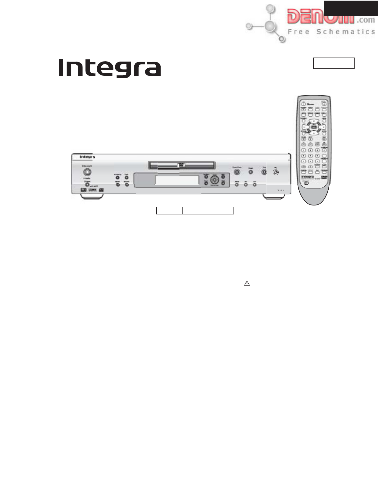
DVD Player
DPS-5.2
DPS-5.2
Ref. No.3686
Jul, 2001
MDD 120V AC, 60Hz
SAFETY-RELATED COMPONENT WARNING!!
COMPONENTS IDENTIFIED BY MARK ON THE
SCHEMATIC DIAGRAM AND IN THE PARTS LIST ARE
CRITICAL FOR RISK OF FIRE AND ELECTRIC SHOCK.
REPLACE THESE COMPONENTS WITH ONKYO
PARTS WHOSE PART NUMBERS APPEAR AS SHOWN
IN THIS MANUAL.
MAKE LEAKAGE-CURRENT OR RESISTANCE
MEASUREMENTS TO DETERMINE THA T EXPOSED
PARTS ARE ACCEPTABLY INSULATED FROM THE
SUPPLY CIRCUIT BEFORE RETURNING THE
APPLIANCE TO THE CUSTOMER.
RC-451DV
www.denom.com
Page 2

SPECIFICATIONS
DVD Player
Power supply AC 120 V, 60 Hz
Power consumption 14 W
Weight 3.4 kg, 7.5 lbs.
External dimensions 435 x 91 x 312 mm (W/H/D), 17-1/8" x 3-9/16" x 12-5/16"
Signal system Standard NTSC
Regional restriction code 1
Laser Semiconductor laser, wavelength 650 nm
Frequency range (digital audio) DVD linear sound: 48 kHz sampling 4 Hz to 22 kHz
96 kHz sampling 4 Hz to 44 kHz
Audio CD: 4 Hz to 20 kHz
Signal-to-noise ratio (digital audio) More than 100 dB
Audio dynamic range (digital audio) More than 96 dB
Harmonic distortion (digital audio) Less than 0.015 %
Wow and flutter Below measurable level (less than ±0.001 % (W.PEAK))
Operating conditions Temperature: 5 C to 35 C (41 F to 95 F), Operation status: Horizontal
DPS-5.2
Outputs
Video output 1.0 V (p-p), 75 ohm , negative sync., pin jack 1
S-video output (Y) 1.0 V (p-p), 75 ohm , negative sync., Mini DIN 4-pin 1
(C) 0.286 V (p-p), 75 ohm
Component video output (Y) 1.0 V (p-p), 75 ohm , negative sync., pin jack 1
B)/(PR) 0.7 V (p-p), 75 ohm
(P
Audio output (digital output Optical) 22.5 dBm 1
Audio output (digital output Coaxial) 0.5 V (p-p), 75 ohm , pin jack 1
Audio output (analog audio) 2.0 V (rms), 470 ohm , pin jack (L, R) 2
Audio output (Mono) 2.0 V (rms), 470 ohm , pin jack 1
Specifications and features are subject to change without notice.
-
www.denom.com
Page 3
SERVICE GUIDE 1
DPS-5.2
WARNING:
TO REDUCE THE RISK OF FIRE OR ELECTRIC SHOCK,
DO NOT EXPOSE THIS APPLIANCE TO RAIN OR
MOISTURE.
CAUTION:
TO REDUCE THE RISK OF ELECTRIC SHOCK, DO NOT
REMOVE COVER (OR BACK). NO USER-SERVICEABLE
PARTS INSIDE. REFER SERVICING TO QUALIFIED
SERVICE PERSONNEL.
This unit contains a semiconductor laser system and is classified
as a "CLASS 1 LASER PRODUCT". So, to use this model
properly, read this Instruction Manual carefully. In case of any
trouble, please contact the store where you purchased the unit.
To prevent being exposed to the laser beam, do not try to open
the enclosure.
CAUTION:
VISIBLE LASER RADIATION WHEN OPEN AND INTERLOCK
FAILED OR DEFEATED. DO NOT STARE INTO BEAM.
CAUTION:
THIS PRODUCT UTILIZES A LASER. USE OF CONTROLS OR
ADJUSTMENTS OR PERFORMANCE OF PROCEDURES
OTHER THAN THOSE SPECIFIED HEREIN MAY RESULT IN
HAZARDOUS RADIATION EXPOSURE.
WARNING
RISK OF ELECTRIC SHOCK
DO NOT OPEN
The lightning flash with arrowhead symbol, within an equilateral
triangle, is intended to alert the user to the presence of uninsulated
"dangerous voltage" within the product's enclosure that may be of
sufficient magnitude to constitute a risk of electric shock to persons.
The exclamation point within an equilateral triangle is intended to alert
the user to the presence of important operating and maintenance
(servicing) instructions in the literature accompanying the appliance.
The label on the right
is applied on the rear
panel except for USA
and Canadian
models.
1.This unit is a CLASS 1 LASER PRODUCT and employs a
laser inside the cabinet.
2.To prevent the laser from being exposed, do not remove
the cover. Refer servicing to qualified personnel.
"CLASS 1 LASER
PRODUCT
AVIS
RISQUE DE CHOC ELECTRIQUE
NE PAS
OUVRIR
"
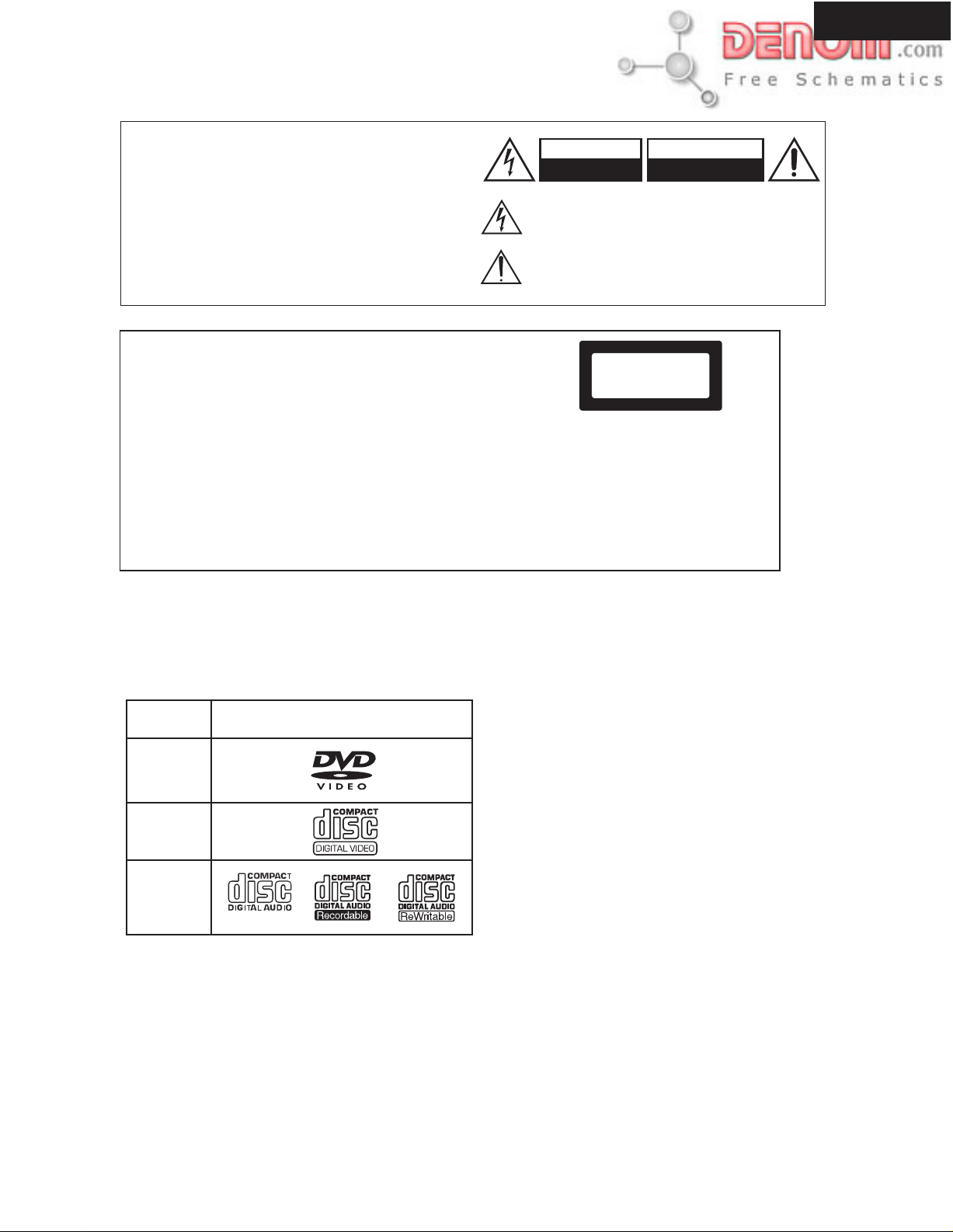
NOTES ON DISC
Playable Discs
Playable Disc
This DVD Player can playback the following discs.
Disc mark
DVD videos
VIDEO CDs
*1 *1
Audio CDs
*1This unit can play CD-R and CD-RW discs recorded in CD
Audio or Video CD format, or with MP3 audio files.
*You cannot playback discs other than those listed above.
You cannot play discs such as CD-ROM, DVD-RAM, DVDRW, etc., even if the marks in the above table are labeled
on those discs.
*This DVD Player uses the PAL/NTSC color system, and
cannot playback DVD videos recorded in any other color
system (SECAM, etc.).
*Avoid using heart-shaped or octagonal discs. Playing
irregularly shaped discs may damage the internal
mechanism of the DVD Player
.
About VIDEO CDs
CDs
This DVD Player supports VIDEO CDs equipped with the PBC
(Version 2.0) function. (PBC is the abbreviation of Playback Control.)
You can enjoy two playback variations depending on the type of disc.
* VIDEO CD not equipped with PBC function (Version 1.1)
Sound and movies can be played on this DVD Player in the
same way as an audio CD.
* VIDEO CD equipped with PBC function (Version 2.0)
In addition to operation of the VIDEO CD not equipped with the
PBC function, you can enjoy playback with interactive software
and search function using the menu displayed on the TV
screen (Menu Playback). Some of the functions described in
this Instruction Manual may not work with some discs.
www.denom.com
Page 4

P ANEL VIEW
FRONT PANEL
DPS-5.1
1
2 3 4 5
14 15 16 17 18
Power switch and Standby indicator
1
Turns on the main power supply for the DPS-5.2. The DPS-5.2
enters standby state and the Standby indicator lights up. Pressing
the switch again to the off position (Off) shuts down the main
power supply into the DPS-5.2.
• Before turning on the power, make sure all cables are properly
connected.
Standby/On button
2
When Standby/On button is pressed to On while the Power
switch is set to On, the DPS-5.2 turns on and the Standby
indicator turns off. Pressing the button again returns the DPS-5.2
to the standby state.
Last Memory button
3
You can resume DVD or Video CD playback from the point you
last watched even if the disc is removed from the player. Press
Last Memory during playback to set a Last Memory point. When
you want to resume playback of that disc, press Last Memory in
the stop mode and playback starts from the memorized point.
Last Memory locations can be stored for up to 5 DVDs and 1
Video CD.
Clear button
4
Works in conjunction with a number of player functions. Use to
cancel repeat and random playback, and to edit programs.
5
Remote control sensor
Point the remote control toward the remote sensor to operate the
player.
Disc tray
6
When loading a disc, place discs in the disc tray with the label
side facing up.
Top Menu button
7
Press to call up the top menu programmed on the DVD.
Depending on the DVD, the top menu may be identical to the
DVD menu.
6 7
8 9 10
11
12 13
19
Cursor ( / / / ) button/Enter button
8
Use to move through the options on menu screens and
///
to change settings. Use Enter to implement settings selected with
the cursor buttons or to set items highlighted in a menu.
9
Menu button
Use to display or close the DVD menu or MP3 Navigator screen.
Open/Close button
10
Press to open and close the disc tray.
Pause button
11
Press during playback to pause. Press again to resume playback.
12
Stop button
Press to stop playback. Pressing once enables playback to
resume from a point shortly before the location where it stopped.
Pressing twice causes the disc to return to the beginning of the
disc if playback starts again.
Play button
13
Press to start or resume playback.
14
Repeat button
Use to set the repeat mode.
15
Random button
Press to play chapters/tracks in random order.
16
Return button
Use to go one menu back (current settings are maintained). Use
RETURN when you do not want to change the option setting in a
menu.
17
Setup button
Press when the player is in either play or stop mode to open and
close the Setup screen.
18
Display button
Press during playback to display statistical disc information.
Press repeatedly to display different information.
/ button
19
Press to go back or advance to previous chapters/tracks. Press
and hold to perform fast-reverse/fast-forward playback scanning.
www.denom.com
Page 5
SERVICE GUIDE 2
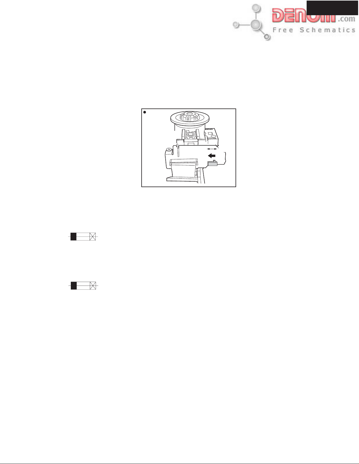
1. Laser diode shorting
1-1 Remove the top cover.
1-2 Laser diode shorting switch is "S" position. (Fig-1)
1-3 Remove three FFCs.
Rear View
DVDM Assy
Side
Short
DPS-5.2
Open
Short SW
Fig.-1
2. Replacing the fuse
THIS SYMBOL LOCATED NEAR THE FUSE INDICATES
THAT THE FUSE USED IS SLOW OPERATING TYPE
FOR CONTINUED PROTECTION AGAINST FIRE
HAZARD,REPLACE WITH SAME TYPE FUSE. FOR FUSE
RATING REFER TO THE MARKING ADJACENT TO THE SYMBOL
CE SYMBOLE INDIQUE QUE LE FUSIBLE UTLISE EST
E LENT. POUR UNE PROTECTION PERMANENTE,N'UTILISER
QUE DES FUSIBLES DE MEME TYPE. CE DARNIER EST
INDIQUE LA QU LE PRESENT SYMBOL EST APPOSE.
CIRCUIT NO. PART NO. DESCRIPTION
F1 252252 or
252147
1.6A-T/UL-ST2 or
1.6A-TSC
www.denom.com
Page 6
PANEL VIEW
Display
DPS-5.2
12345 67 89
Rear panel
DVD VC D
D
DTS
GUI
TITLE CHAPTER TRACK REMAIN
101112
/ indicator
1
Inserted disc indicator
2
3
TITLE indicator
4
Angle icon indicator
5
CHAPTER/TRACK indicator
6
REPEAT indicator
7
REMAIN indicator
1234 5 78
RS-232
OUTPUT
VIDEO
S VIDEO
VIDEO
COMPONENT
REPEAT
LAST
COND.
13
LAST indicator
8
9
COND. indicator
10
D indicator
11
DTS indicator
12
GUI indicator
13
Multifunctional indicator
(e.g. operating status and error messages)
6 9
ANALOG
OUTPUT
MONO
Y
P
B
L
RLR
P
R
OPTICAL
DIGITAL
OUTPUT
COAXIAL
REMOTE
CONTROL
DVD PLAYER
MODEL NO.
DPS-5.2
AC INLET
1.
RS-232 port
This port is to be used in conjunction with an external controller to
control the operation of the DPS-5.2 using an external device.
VIDEO OUTPUT VIDEO jack
2.
Connect to the video input on a TV or monitor or AV amplifier or
receiver with video input capability.
VIDEO OUTPUT S VIDEO jack
3.
If your TV or monitor has an S video input, clear picture
reproduction is possible by connecting the player to your TV or
monitor via the S Video jack.
You can switch between [S1] and [S2] S-video output from the
Setup menu.
4.
VIDEO OUTPUT COMPONENT jacks
If your TV or monitor has component video inputs, you can
produce a higher quality picture on your TV or monitor by
connecting to the component video outputs on this unit.
5.
ANALOG OUTPUT jacks
Use to output two-channel audio (analog) to the audio stereo
inputs on a TV or stereo amplifier. If you are connecting to a
receiver that has both digital and analog input jacks for DVD
player connection, it may be beneficial to make both connections.
www.denom.com
6.
DIGITAL OUTPUT OPTICAL jack
Use to output the digital audio signal recorded on discs. You can
output the digital signal via the optical output jack to an AV
amplifier or receiver.
DIGITAL OUTPUT COAXIAL jack
7.
Use to output the digital audio signal recorded on discs. You can
output the digital signal via the coaxial output jack to an AV
amplifier or receiver.
jack
8.
Use to connect this player to another component bearing the
mark. This lets you control this unit as though it were a
component in a system.
9.AC INLET
Use to connect the power cord to the wall outlet.
Page 7

REMOTE CONTROLLER
TV
ON / STANDBY
AUDIO SUBTITLE
ANGLE
COND. M
+
VOL
ENTER
-
VOL
STOPPAUSE PLAY
DOWN UPFR FF
23
SEARCH
0
-
RC
451
DV
TV
OPEN
/CLOSE
MENU
+
CH
SETUPRETURN
STEP/ SLOW
+
-
FUNCTION M
CLEAR
PROGRAM
11
14
1
2
3
4
5
6
7
8
9
10
12
13
ON
STANDBY
LAST M DIMMER DISPLAY
TOP MENU
-
CH
TV/ VCR
1
456
789
+
10
RANDOM REPEAT A-B
REMOTE CONTROLLER
DVD
15
16
18
20
22
23
24
25
26
27
29
31
17
19
21
28
30
FR/FF / buttons
11
During playback of DVD and Video CD, press to perform fast
forward scanning or to perform fast reverse scanning of DVD
and Video CD. When a CD or MP3 is loaded, audio scanning is
performed.
Number buttons (1-9, 0, +10)*
12
Use to perform direct title/folder and chapter/track searches, and
to input numerical values.
13
RANDOM button
Press to play chapters/tracks in random order.
REPEAT button
14
Use to set the repeat mode.
button
15
Press to open or close the disc tray.
SUBTITLE button
16
Press repeatedly to select one of the subtitle languages
programmed on a DVD or to turn the subtitles off.
17
AUDIO button
Press repeatedly to select one of the audio languages
programmed on a DVD.
For Video CD, CD and MP3, each press changes the audio
output as follows.
Stereo 1L(Left) 2/R(Right)
DPS-5.2
1
ON button
Press to switch the player on.
2
STANDBY button
Press to put the player in standby.
3
ANGLE button
Some DVDs are recorded with various camera angle playback
options. Press ANGLE repeatedly to display different camera
angles.
4
LAST M button
You can resume DVD or Video CD playback from the point you
last watched even if the disc is removed from the player. Press
LAST M during playback to set a Last Memory point. When you
want to resume playback of that disc, press LAST M in the stop
mode and playback starts from the memorized point. Last Memory
locations can be stored for up to 5 DVDs and 1 Video CD.
5
COND. M button
You can store in memory the settings for up to 15 DVDs. Press
COND. M during DVD playback to memorize the settings.
6
TOP MENU button*
Press to call up the top menu programmed on the DVD.
Depending on the DVD, the top menu may be identical to the DVD
menu.
7
Cursor buttons ( / / / )*
///
VOL +/- buttons
Use to move through the options on menu screens and to change
settings.
CH +/- , VOL +/- buttons
8
RETURN button*
Use to go one menu back (current settings are maintained). Use
RETURN when you do not want to change the option setting in a
menu.
TV/VCR button
9
PAUSE button
Press to pause playback of a disc. Press again to resume
playback.
10
STOP button
Press to stop playback. Pressing once enables playback to
resume from a point shortly before the location where it was
stopped. Pressing twice causes the disc to return to the beginning
of the disc when playback starts again.
18
DISPLAY button
Press during playback to display statistical disc information.
Press repeatedly to display different information.
19
DIMMER button
Toggle to control the lightness of the display.
20
MENU button*
Use to display or close the DVD menu or MP3 Navigator screen.
ENTER button*
21
Use to implement settings selected with the cursor buttons or to
set items highlighted in a menu.
22
SETUP button*
Press when the player is in either play or stop mode to open and
close the Setup screen.
23
PLAY
Press to start or resume playback.
24
UP/DOWN /
During playback, press to go back to a previous chapter/track
and to advance to the next chapter/track .
25
STEP/SLOW +/- buttons
Press STEP/SLOW + or Ð during playback to view still frame.
Press and hold STEP/SLOW + or Ð during playback to view slow
playback. In still frame, press STEP/SLOW + to advance DVDs
and Video CDs frame by frame and STEP/SLOW Ð to back up a
few frames at a time (DVD only).
26
FUNCTION M button
You can store in memory up to 5 settings. Press FUNCTION M to
memorize and recall the settings.
CLEAR button
27
Works in conjunction with a number of player functions. Use to
cancel repeat and random playback, and to edit programs.
SEARCH button
28
Press to perform a title/folder, chapter/track or elapsed time
search.
29
PROGRAM button
You can program titles, chapters, or tracks to play back in a
desired order. Programs can be a maximum of 24 steps.
Additionally, DVD programs for up to 24 discs can be stored in
the player'ss memory for future use.
A-B button
30
Press at the beginning and end of the section you want to repeat
or to mark a location you want to return to.
31
DVD/TV switch
(Buttons indicated with * are used for menu operation.)
www.denom.com
Page 8

EXPLODED VIEW
DPS-5.2
53
52
53
F1
U10
51
53
101
53
16
53
53
E702
E751
U7
E903
Z11
13
Z12
To DVD
Mechanism
U1
Z14
Z13
Z14
Z10
23
15
U5
13
U6
31
D
V
D
33
37
35
37
37
E701
23
23
U2
23
19
23
41
S731
54
55
25
U3
1
17
20
56
27
U9
23
105
21
49
45
3
3
9
5
11
5
7
43
49
7
www.denom.com
Page 9
EXPLODED VIEW PARTS LIST
DPS-5.2
REF. NO.
11 27191112 KGPS-6RF
13 838130208 3TTB+20B, Self tapping screw
15 29362584 Label (DVD)
16 29363012 Label, RISK
17 28325753 Knob
19 27111221A Front bracket
20 29110161 Ta
21 28191928 Clear
23 838130088 3TTB+8B, Self tapping screw
25 82143010 3P+10FN
27 28325933 Knob, CRS
31 28148479 Door
33 27262651 Plate
35 28184808 Top cover
37 838430088 3TTB+8B
41 27212326 Front
43 28135278 Badge
45 28198906 Facet
49 838430088 3TTB+8B
51 27122865 Rear panel
52 838440089 4TTB+8C
54 838126088 2.6TTB+8B, Self tapping screw
55 27191142A Holder, PLATE
56 28133398 Back plate
105 28325756 Knob (STANDBY
E701 2045222012 NCFC5-222012, Flexible flat cable
E702 2009990691UL NSAS-10P0959, Socket AS
E751 2045081212 NCFC5-081212
E903 260208 Wire tie
F1 252252 or 1.6A-T/UL-ST2 or
F1 252147 1.6A-TSC, Fuse
S731 25035710 NPS-115-S673, Joy switch
U1 1H474581-1G NAAR-7181-1G, Output terminal
U2 1H474582-1G NADIS-7182-1G, Display circuit
U3 1H474583-1G NADIS-7183-1G, Standby LED
U9 1H474584-1G NAPS-7184-1G, AC Inlet terminal
U5 1H474585-1G NAETC-7185-1G, Support PC board
U6 1H474586-1G NASW-7186-1G, Power switch
U7 1H474588-1G NAETC-7188-1G, RS-232C connector
U10 24150020A NGPS-0020-120V, Power supply unit
Z10 24150019 DB-VPB301, Main circuit PC board assy
Z11 24801010 DB-VLD301-006, DVD mechanism
Z12 24840149A DB-VAC301, Adapter L
Z13 24840150A DB-VAC302, Adapter R
Z14 838130088 3TTB+8B, Self tapping screw
PART NO. DESCRIPTION
1 27100399A Chassis
3 27175316B Leg
5 28141332 Cushion
7 838130088 3TTB+8B
9 27190428A KGLS-10RF, Holder
PC board assy
PC board assy
PC board assy
PC board assy
PC board assy
PC board assy
, Self tapping screw
,Holder
Part No. 29362648
(POWER)
pe CU
plate
(BC), Self tapping screw
(BC), Self tapping screw
panel
(BC), Self tapping screw
(BC), Self tapping screw
)
, Flexible flat cable
NOTE: THE COMPONENTS IDENTIFIED BY MARK
ARE CRITICAL FOR RISK OF FIRE AND
ELECTRIC SHOCK. REPLACE ONLY WITH
PART NUMBER SPECIFIED.
www.denom.com
Page 10
EXPLODED VIEW (LOADING MECHANISM)
DPS-5.2
2
23
Daifree
GEM1036
15
14
Lubricating Oil
12
GYA1001
13
6
To DVDM
CN151
8
8
8
8
20
18
17
16
19
A
10
11
Lubricating Oil
GYA1001
9
1
LOADING MECHANISM PARTS LIST
REF.NO. PART NO.
1 VNP1836 Loading PC board assy
2 VXX2782 Traverse mechanism assy-S
6 VDA1864 Flexible cable 26P
8 VEB1327 Float rubber
9 VEB1328 Belt
10 VNE2253 Stabilizer
11 VNL1917 Loading base
DESCRIPTION
www.denom.com
REF.NO. PART NO.
DESCRIPTION
12 VNL1918 Float base DVD
13 VNL1919 Drive cam
14 VNL1921 Gear pulley
15 VNL1922 Loading gear
16 VNL1923 Drive gear
17 VNL1925 SW lever
18 VNE2251 Clamper plate
19 VNE2252 Bridge
20 VNL1924 Clamper
23 VNL1920 Tray
Page 11
A
BLOCK DIAGRAM
BCDEFGH
1
Overall
Main circuit PCB
DB-VPB301
CN151
(26P)
RF
B1
B2
B3
B4
(RF)
RF
16
7
6
12
11
3
B1
B2
B3
B4
6
LA9701M
7
8
9
IC101
RF IC
54
46
56
57
42
35
Spindle
Motor
Pickup
Assembly
(26P)
11
20
21
15
16
2
T DRV
25
T RTN
24
F DRV
23
F RTN
26
CN1
(12P)
9
8
7
6
5
4
3
4
3
M
Stepping
Motor
(Carriage)
CN2
(4P)
2
1
CN3
(17P)
10
11
12
13
14
H1+
9
H1-
H2+
H2-
H3+
H3-
ST1+
1
ST1-
2
ST2+
4
ST2-
5
2
3
4
1
9
10
11
12
13
14
1
2
4
5
CN61
(17P)
T DRV
T RTN
F DRV
F RTN
12
IC351
13
M56788AFP
9
FTS Driver
10
35 34 31 32 15 14
(RF) (RF)
RFO
DSP RF
(RF)
BH
PH
FE
TE
32 33 30 31 39 3
FDO
3
TDO
20
9
10
11
12
13
14
IC251
BA6664FM
Spindle
Driver
47
LC78652W
48
Servo DSP IC
SPDO
21
IC201
(RF)
46 14
ROMXA
16M
(AD)
33M
16M
(AD)
PD6345A
System Control
57
LODPOS
SSIB ASSY
CN602
(2P)
+-
M
Loading
Motor
Assy
LOAB ASSY
4
2
1
S101
Loading
Position
Switch
CN601
AC IN
(5P)
1
2
4
NEUTRAL
CN52
(5P)
LOD- LOD-
1
LOD+ LOD+
2
SW2 LODPOS
4
CN1
(2P)
1
LIVE
F1
2
CN2
(14P)
V+12D V+12M
V+5DV+5VV+5S
V+3D
V12M
SW+5
V3VD
V+6M
29 22
28,30 21,23
2
(14P)
-27V
EV+5V
1,3 8,10
P902
-27V
14
10
1
EV+5V
5
+6V
7
8
+12V
9
6
+5V
11
4
+3.3V
13
2
9
V+5V
V+3V
V+6M
V+12V
P701A
(22P)
IC712
MSM51V17805D-60TS
16M DRAM
170
112
IC701
PE5108A
4
DVD Decoder
107
BY Chip
IC601
105
X48/44
27M
(for IC801)
3
X48/44
14 15
CN401 (2/2)
(30P)
CN102 (2/2)
(30P)
IR
SEL IR
Clock Generator
10
22/24M
(for IC211)
CONTROLCONTROLCONTROL
(VD) (VD)
57-60
63-66
111
IC603
VYW1853
8M Flash Memory
16M
(for IC201, IC701)
13
IC481
BU2288FV
9
36/16M
(for IC801)
P354
CONTROL
EV+5V
-27V
SD0-SD7
CDDATA
33M
(for IC701)
U10: POWER
SUPPLY
UNIT
U3: Standby LED PCB
NADIS-7183A
JL771B
5
Key switck
(5P)
JL771A
1
2
(5P)
KEY SW
P701B
(22P)
Q701
MPD780232GC
FL Control IC
IR
E+5V
-27V
FLAC2
FLAC1
Q702
FL Tube
Q705
Remote
Receiver
Unit
(7P)
P731
Jog switch
PCB
(7P)
P731
www.denom.com
U2: Display circuit PCB
NADIS-7182A
Page 12

DPS-5.2
IC805
MB81F161622C-80FN
16M SDRAM
(VD)
149,150,
152-155,
158,159
48
IC801
M65774BFP
MPEG2 Decoder
AV-1
5564
27M36/16M
(RF)
: RF SIGNAL ROUTE
(AD)
: AUDIO DATA SIGNAL ROUTE
: AUDIO SIGNAL ROUTE
(D)
: AUDIO (DIGITAL) SIGNAL ROUTE
(D)
(D)
DOUT0
74
ADA0A
68
PD0-PD7
95-98,
100-103
(VD)
93
27M
Cr/R
24
Y/G
2-9
48
IC861
28
Cb/B
25
V
35
Y
33
C
29
(VD)
27M
ADV7172KST
Video Encoder
U1: Output terminal PCB
(VD)
: VIDEO DATA SIGNAL ROUTE
: VIDEO SIGNAL ROUTE
(V)
: V SIGNAL ROUTE
(Y)
: Y SIGNAL ROUTE
CN401 (1/2)
(30P)
DOUT0
22/24M
Q911
Q913
Q902
CN15
(30P)
5 26
7
2
29
27
25
26
30
28
(D) (D) (D)
Q912
Q901
Q903
DOUT
ADATA0
Cr/R
Y/G
Cb/B
V
Y
C
CN102 (1/2)
(30P)
CN106
(30P)
7
22/24M
2
Cr/R
29
Y/G
27
Cb/B
25
26
30
28
Q301
PCM1742KE
192kHz, 24bit
2ch DAC
7
2
8
16
(R)
(Y)
(B)
V
(V)
(Y)
Y
C
(C)
MM1540BF
6ch Amp.
Driver with LPF
13
9
11
2
6
4
Q201
NAAR-7181
(C)
: C SIGNAL ROUTE
(R)
: R SIGNAL ROUTE
(G)
: G SIGNAL ROUTE
(B)
: B SIGNAL ROUTE
(D)
Q601
Q401/402
NJM4565M-D
(V)
V
27
(Y)
Y
23
C
(C)
25
Cr/R
16
Y/G
20
Cb/B
18
(G)
(D)
(Y)
Y
C
(C)
AUDIO_L
AUDIO_R
(R)
(B)
P751A
V
C
Y
R
G
B
Q352
OPTICAL
COAXIAL
P353
JA201
L
R
Mono
P201
Composite
P203
(22P)
DIGITAL
AUDIO
S VIDEO
V
COMPOSITE
Video
component
Not used
GND
REQ
BUSY
SDATAIN
SCK
SDATAOUT
RESET
U7:RS-232C connector
PC board
NAETC-7188
Q801:
MPD789071MC
P751B
8 bit
microprocessor
Q802:
MPD4721GS
Driver/
Receiver
P801
www.denom.com
Page 13
DPS-5.2
A
BCDEFGH
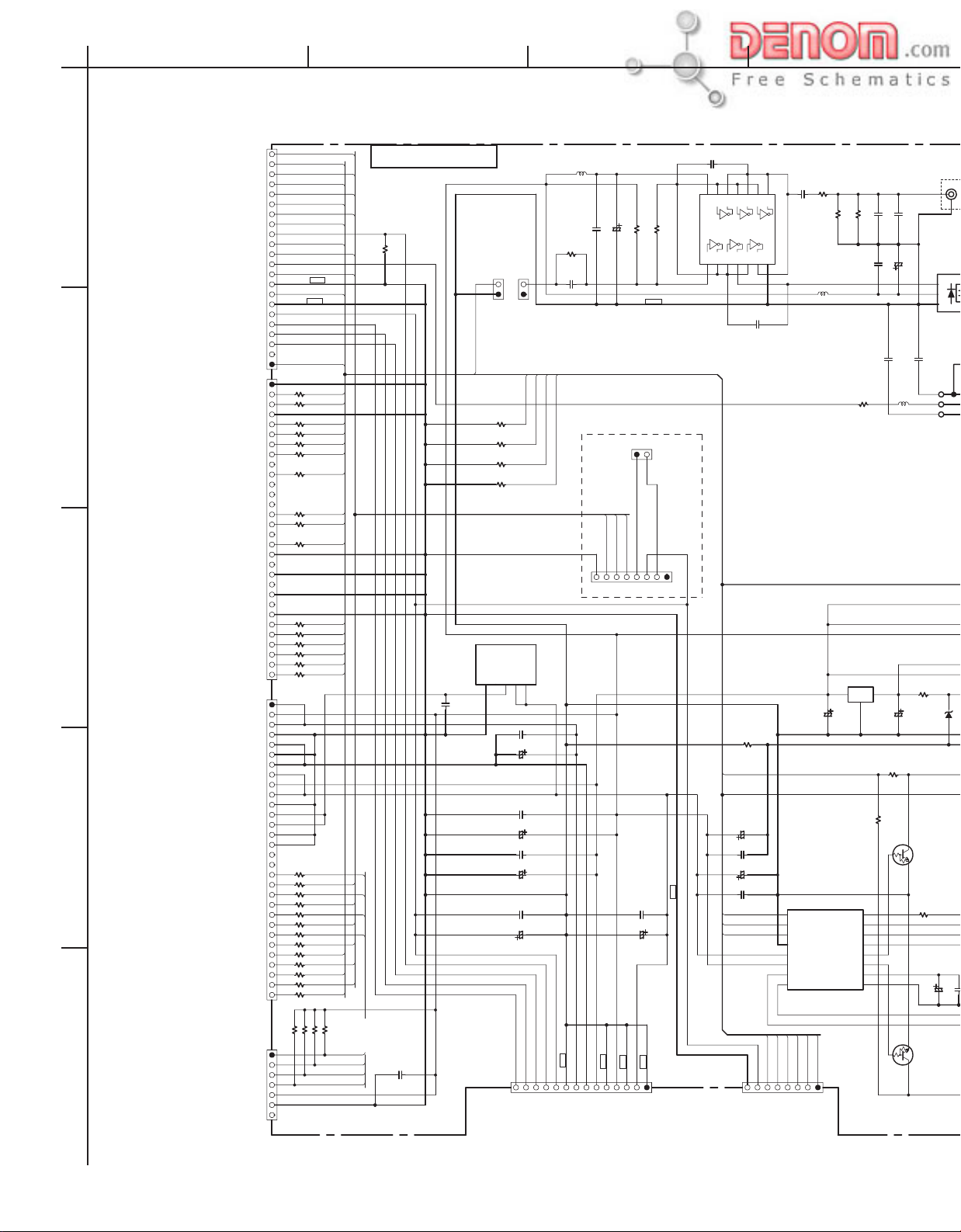
SCHEMATIC DIAGRAM
P701A
SCK
22
232SO
21
SI
1
2
P/XI[VSEL2]
3
232SCK
SO
232SI
XRDY
232BU
PON
232RE
RESET
RI
LT1
GND2
VCOFF
GND1
EVER+5V
-27V
FLAC1
FLAC2
NC
SRESET
CN106
GND1
MCLK
BCK
GND2
LRCK
XCSDF
ADATA0
XSCK
ADATA1
XSI
ADATA2
6CH/X2CH
ADATA3
XMUTE
VSEL1
LFE_ON
GND3
PRG_CR
GND4
PRG_CB
GND5
PRG_Y
GND6
B/CB
V
G/Y
C
R/CR
Y
20
19
18
17
16
15
14
13
12
11
10
9
8
7
6
5
4
3
2
1
1
2
3
4
5
6
7
8
9
10
11
12
13
14
15
16
17
18
19
20
21
22
23
24
25
26
27
28
29
30
SCK
232SO
SI
232SCK SW+5V
SO
232SI
XREADY
232BU
P_ON SQUEEZE
232RE
XRESET
RI
LT
GND
VCOFF
GND
EVER+5V
-27V
FLAC1
FLAC2
232RESET V V+8V
47
R102
MCLK
R103
47
BCK
47
R104
LRCLK Y
R105
47
XCSDF
R106
47
ADATA0
47
R107
XSCK
47
R108
XSI
47
R109
XMUTE
47
R110
VSEL1
R111
47
VSEL2 R/CR
47
R112
47
R113
R114
47
47
R115
R116
47
47
R117
CN102
M+6V1
1
SW5V
2
M+6V2
3
GND1
4
GNDM1
5
GND2
6
GNDM2
7
+3.3V1
8
+12VM
9
+3.3V2
10
GND3
11
+2.5V1
12
+2.5V2
13
GND4
4
5
GND5
MICON2
MICON1
CTS
LT1
DTR
XRESET
RXD
S[FTOM]
TXD
S[MTOF]
AODAI
SCK
SQUEEZE
XREADY
LETTER
P104
TXD
RXD
DTR
CTS
V+5D
GNDD
NC
14
15
16
17
18
19
20
21
22
23
24
25
26
27
28
29
30
1
2
3
4
5
6
7
R118
47
R119
47
47
R120
47
R121
R122
47
47
R123
47
R124
47
R125
47
R126
47
R127
47
R128
SQUEEZE
47
R129
XREADY
R130
47
10K
10K
10K
R133
R132
R131
1mm Pich FFC
For Download
XRESET
LETTER
R134 10K
U1:Output Terminal PC board
Q351
TC74VHCU04T
GND
EVER+5V
C361
020
13
14
VCC
12345
C301
100/6.3
R901
0
9
101112
6
XMUTE
C302
104Z
C303
100/6.3
C304
104Z
C354
8
GND7
C362
020
232RE
R353
330
104K
R354
L352
BK1608LM182-T
C911
100/16
BCKIN1
MCLK
DATA2
LRCKIN3MC
GND4
VDD5
ZEROL
VCC6
ZEROR
VOUTL7
VCOM
AGND
VOUTR8
Q301
PCM1742KE
232BU
232SI
232SO
232SCK
232RESET
P751A
180
I
ML
MD
R355
R356
470
Q901
78M08
G
16
15
14
13
12
11
10
9
220
180
C355
C356
104Z
C359
BK1608LM182-T
O
C912
R433
1K
R434
223Z
C357
C358
C360
L353
R902
10K
100/16
Q302
RN 1407
R301
220
RN1407
100/6.3
223Z
D901
C305
Q303
3
2
1
2
3
SW+5V
V+12V
C913
UDZS5.1B
100/6.3
P353
COAXIAL_OUT
OPTICAL_OUT
GP1FA551RZ
Q352
P354
C914
47/16
D401
1SS352
AGND
104Z
C306
D402
1SS352
RI_OUT1
104Z
V+6A
MUTE+12V
V+12V
MUTE+12V
C401
22/50
C402
22/50
1.8K
C452
R431
NC
R435
R403
R404
R436
RN1407
R401
2.2K
R402
2.2K
RN1407
Q419
C403
C404
Q410
LETTER
C201
R405
15K
R406
15K
C
G/Y
B/CB
100/16
R437
C405
C406
R438
C202
R407
10K
221
221
R408
10K
104Z
Q411
2SA1162
R409
33K
2
3
R411
R412
3
2
R410
33K
4.7K
Q412
2SA1162
104Z
C203
C204
104K
C205
C206
104K
C207
104K
C208
C209
104K
C210
10/6.3
C211
104K
C212
C213
104K
C214
C417
C407
330
NJM4565M-D
+B
8
0
100/16
0
100/16
8
+B
NJM4565M-D
C408
330
102
C418
C225
104Z
Q202
RN1407
100K
R289
R290
100K
C215
47/16
RMPOTHERS
R224 0 NC
R225 0 NC
R226 0 NC
R227 0 NC
R228 0 NC
R229 0
C411
22/50
Q401
1
C409
C410
1
Q402
C412
22/50
Q204
RN1407
Q203
RN2403
R201
1.5K
1K
R202
VCC11VCC228
VIN2 VOUT27
YCMIX3
CIN4
CLP5
YIN16
MUTE17
MUTE28
YIN29
GND10
CBIN11 CBOUT18
DUAL12
CRIN13 CROUT16
VEE114 VEE215
C216
104Z
NC
R415
220
6
HN1C03F
Q403
2
1
100K
R413
R417
2.2K
2.2K
R418
1
100K
R414
2
Q404
HN1C03F
6
R416
220
R451R432
PS126
COUT25
VEE624
YOUT123
Q201MM1540BF
VEE522
VEE421
20
YOUT2
VEE319
PS217
R419
220
5
R421
2.2K
C413
102
C414
102
R422
2.2K
5
R420
220
RN1407
R452
R203
3
4
4
3
Q451
Q205
RN2403
0
R225
R224
6
R423
5
1K
Q403
HN1C03F
Q404
HN1C03F
R424
5
1K
6
R226
-B
-B
R453
R227
4
4
C220
470/6.3
C221
470/6.3
C222
470/6.3
R229
R228
R441
1K
7
Q401
NJM4565M-D
Q402
NJM4565M-D
7
R442
1K
C451
2SA1162
Q452
R206
10K
C218
470/6.3
C219
104K
C217
470/6.3
R211
0
R214
0
R219
0
R425
470
R426
470
R212
75
R215
100
R220
100
R217
R222
C415
22/50
R207
75
R209
75
R204
75
470
470
R208
L202
L
L
R210
L
R205
R213
L204
L
R216
L205
L
560
R218
R221
L206
L
560
R223
R428
100K
HN1C03F
Q405
2
R454
220
R429
2.2K
L203
L201
1
HN1C03F
6
R430
Q405
5
R455
220
2.2K
SQUEEZE
NAAR-7181
10K
R101
B/CB C1
V
G/Y Y1
C
R/CR V1
Y
C915
104Z
CTS
LT
DTR
RXD BCK MCLK
SO ADATA0 XCSDF
TXD LRCLK XSCK
SI XSI
DOUT
SCK
TXD
RXD
DTR
CTS
C101
104Z
DOUT
R135
R136
R137
R138
025EZ5M
GND
5NC4
Q902
3
C901
104Z
C903
104Z
C905
104Z
C907
104Z
P351BP351A
ON/OFF2VIN
VOUT
-27V
232SO
1
220/16
FLAC1
232SCK
C902
C904
220/6.3
C906
220/16
C908
220/6.3
FLAC2
232SI
P_ON
L351
R357
0
C351
232BU
GND
EVER+5V
BK1608LM182-T
104Z
C352
P710B
SI
GND
M+5V
MGND
V+12V
100/6.3
R351 100K
R352 470K
C353
GND
for FL Micon DL
SO
SCK
P711
C909
104Z
C910
220/6.3
GND
GND
SW+5V
+3.3V
P902
P201
V+12V
VSEL1
VSEL2
GND
G1
B1
R1
4
3
G1
1
Y
3
G2
5
C
4
G3
2
SW
6
G4
7
SIGNAL
8
P203
4
Y
2
CB
1
GND
3
CR
P250A
V+12V
1
VSEL1
2
C
3
VSEL2
4
Y
5
GNDV1
6
V7
GNDV2
8
G
9
GNDV3
10
B11
GNDV4
12
R
13
GNDV5
14
+5V
15
AUDIO_L
16
GNDA
17
AUDIO_R
18
SQUEEZE
19
V+8V
20
P402
2
L
1
3
R
MONO
3
1
L
2
R
4
P401
www.denom.com
Page 14
A
BCDEFGH
SCHEMATIC DIAGRAM
P701A
SCK
22
232SO
21
SI
1
2
P/XI[VSEL2]
3
232SCK
SO
232SI
XRDY
232BU
PON
232RE
RESET
RI
LT1
GND2
VCOFF
GND1
EVER+5V
-27V
FLAC1
FLAC2
NC
SRESET
CN106
GND1
MCLK
BCK
GND2
LRCK
XCSDF
ADATA0
XSCK
ADATA1
XSI
ADATA2
6CH/X2CH
ADATA3
XMUTE
VSEL1
LFE_ON
GND3
PRG_CR
GND4
PRG_CB
GND5
PRG_Y
GND6
B/CB
V
G/Y
C
R/CR
Y
20
19
18
17
16
15
14
13
12
11
10
9
8
7
6
5
4
3
2
1
1
2
3
4
5
6
7
8
9
10
11
12
13
14
15
16
17
18
19
20
21
22
23
24
25
26
27
28
29
30
SCK
232SO
SI
232SCK SW+5V
SO
232SI
XREADY
232BU
P_ON SQUEEZE
232RE
XRESET
RI
LT
GND
VCOFF
GND
EVER+5V
-27V
FLAC1
FLAC2
232RESET V V+8V
47
R102
MCLK
R103
47
BCK
47
R104
LRCLK Y
R105
47
XCSDF
R106
47
ADATA0
47
R107
XSCK
47
R108
XSI
47
R109
XMUTE
47
R110
VSEL1
R111
47
VSEL2 R/CR
47
R112
47
R113
R114
47
47
R115
R116
47
47
R117
CN102
M+6V1
1
SW5V
2
M+6V2
3
GND1
4
GNDM1
5
GND2
6
GNDM2
7
+3.3V1
8
+12VM
9
+3.3V2
10
GND3
11
+2.5V1
12
+2.5V2
13
GND4
4
5
GND5
MICON2
MICON1
CTS
LT1
DTR
XRESET
RXD
S[FTOM]
TXD
S[MTOF]
AODAI
SCK
SQUEEZE
XREADY
LETTER
P104
TXD
RXD
DTR
CTS
V+5D
GNDD
NC
14
15
16
17
18
19
20
21
22
23
24
25
26
27
28
29
30
1
2
3
4
5
6
7
R118
47
R119
47
47
R120
47
R121
R122
47
47
R123
47
R124
47
R125
47
R126
47
R127
47
R128
SQUEEZE
47
R129
XREADY
R130
47
10K
10K
10K
R133
R132
R131
1mm Pich FFC
For Download
XRESET
LETTER
R134 10K
U1:Output Terminal PC board
Q351
TC74VHCU04T
GND
EVER+5V
C361
020
13
14
VCC
12345
C301
100/6.3
R901
0
9
101112
6
XMUTE
C302
104Z
C303
100/6.3
C304
104Z
C354
8
GND7
C362
020
232RE
R353
330
104K
R354
L352
BK1608LM182-T
C911
100/16
BCKIN1
MCLK
DATA2
LRCKIN3MC
GND4
VDD5
ZEROL
VCC6
ZEROR
VOUTL7
VCOM
AGND
VOUTR8
Q301
PCM1742KE
232BU
232SI
232SO
232SCK
232RESET
P751A
180
I
ML
MD
R355
R356
470
Q901
78M08
G
16
15
14
13
12
11
10
9
220
180
C355
C356
104Z
C359
BK1608LM182-T
O
C912
R433
1K
R434
223Z
C357
C358
C360
L353
R902
10K
100/16
Q302
RN 1407
R301
220
RN1407
100/6.3
223Z
D901
C305
Q303
3
2
1
2
3
SW+5V
V+12V
UDZS5.1B
100/6.3
NAAR-7181
10K
R101
B/CB C1
V
G/Y Y1
C
R/CR V1
Y
C915
104Z
CTS
LT
DTR
RXD BCK MCLK
SO ADATA0 XCSDF
TXD LRCLK XSCK
SI XSI
DOUT
SCK
TXD
RXD
DTR
CTS
C101
104Z
DOUT
R135
R136
R137
R138
025EZ5M
GND
5NC4
Q902
3
C901
104Z
C903
104Z
C905
104Z
C907
104Z
P351BP351A
ON/OFF2VIN
VOUT
-27V
232SO
1
220/16
FLAC1
232SCK
C902
C904
220/6.3
C906
220/16
C908
220/6.3
FLAC2
232SI
P_ON
L351
R357
0
C351
232BU
GND
EVER+5V
BK1608LM182-T
104Z
C352
P710B
SI
GND
M+5V
MGND
V+12V
100/6.3
R351 100K
R352 470K
C353
GND
for FL Micon DL
SO
SCK
P711
C909
104Z
C910
220/6.3
GND
GND
SW+5V
+3.3V
P902
www.denom.com
Page 15

3
2
1
2
3
SW+5V
V+12V
C913
UDZS5.1B
100/6.3
P353
COAXIAL_OUT
OPTICAL_OUT
GP1FA551RZ
Q352
P354
C914
47/16
D401
1SS352
AGND
104Z
C306
D402
1SS352
RI_OUT1
104Z
V+6A
MUTE+12V
V+12V
MUTE+12V
1.8K
C452
C401
22/50
C402
22/50
R431
NC
R403
R404
RN1407
R435
R401
2.2K
R402
2.2K
R436
Q419
C403
C404
Q410
RN1407
LETTER
C201
R405
15K
R406
15K
C
G/Y
B/CB
100/16
R437
C405
C406
R438
C202
R407
10K
221
221
R408
10K
104Z
Q411
2SA1162
R409
33K
R411
R412
R410
33K
4.7K
Q412
2SA1162
104Z
C203
C204
104K
C205
C206
104K
C207
104K
C208
C209
104K
C210
10/6.3
C211
104K
C212
C213
104K
C214
C417
C407
NJM4565M-D
2
+B
8
3
0
0
3
8
+B
2
NJM4565M-D
C408
102
C418
C225
C215
330
Q401
1
C409
100/16
C410
100/16
1
Q402
330
R289
R290
47/16
104Z
RN1407
100K
100K
R224 0 NC
R225 0 NC
R226 0 NC
R227 0 NC
R228 0 NC
R229 0
C411
22/50
C412
22/50
Q204
RN1407
Q202
RMPOTHERS
R413
R414
Q203
RN2403
R201
1.5K
1K
R202
VCC11VCC228
VIN2 VOUT27
PS126
YCMIX3
CIN4
COUT25
CLP5
VEE624
YIN16
YOUT123
Q201MM1540BF
VEE522
MUTE17
VEE421
MUTE28
YIN29
YOUT2
VEE319
GND10
CBIN11 CBOUT18
DUAL12
PS217
CRIN13 CROUT16
VEE114 VEE215
C216
104Z
NC
R415
220
HN1C03F
Q403
100K
100K
Q404
HN1C03F
R416
220
2
R417
R418
2
2.2K
2.2K
R419
220
6
R421
2.2K
1
1
R422
2.2K
6
R420
220
R452
R451R432
5
C413
102
C414
102
5
20
3
4
4
3
Q451
RN1407
R203
Q403
HN1C03F
Q404
HN1C03F
Q205
RN2403
0
R224
R423
1K
R424
1K
R225
6
5
5
6
R453
R226
-B
-B
R227
4
4
2SA1162
C220
470/6.3
C221
470/6.3
C222
470/6.3
R229
R228
R441
1K
7
Q401
NJM4565M-D
Q402
NJM4565M-D
7
R442
1K
C451
Q452
R206
10K
C218
470/6.3
C219
104K
C217
470/6.3
R211
0
R214
0
R219
0
R425
470
R426
470
R212
75
R215
100
R220
100
22/50
R217
R222
C415
R207
75
R209
75
R204
75
470
470
R208
L202
L
L
R210
L
R205
R213
L204
L
R216
L205
L
560
R218
R221
L206
L
560
R223
R428
100K
HN1C03F
Q405
2
R454
220
R429
2.2K
L203
L201
1
HN1C03F
6
R430
Q405
5
R455
220
2.2K
P201
1
3
5
4
2
6
7
8
4
2
1
3
V+12V
VSEL1
VSEL2
GND
G1
B1
R1
SQUEEZE
4
3
2
1
3
3
1
2
4
P203
P250A
V+12V
1
VSEL1
2
C
3
VSEL2
4
Y
5
GNDV1
6
V7
GNDV2
8
G
9
GNDV3
10
B11
GNDV4
12
R
13
GNDV5
14
+5V
15
AUDIO_L
16
GNDA
17
AUDIO_R
18
SQUEEZE
19
V+8V
20
P402
P401
G1
Y
G2
C
G3
SW
G4
SIGNAL
Y
CB
GND
CR
L
R
MONO
L
R
DPS-5.2
www.denom.com
Page 16

DPS-5.2
A
BCDEFGH
SCHEMATIC DIAGRAM
U2:Display circuit PC board
1
2
3
NADIS-7182A
1K
R725
R727R726
Destination
MDD1N
192_L K2
96_L INIT1
PLY_L SYSOUT
STP_L VCOFF
OPC_L LT1
R785
P15 PON
P14 XRDY
P13 SO
P12 SI
P11 XSCK
P10
P9
P8
P7
Q723
R721R720
10K 56K
R790
10K
R789
10K
K0
24
25
+5V
VDD0
K1
21
23
K022K1
K2
VSS0
INIT1
GND2
VCOFF
LT1
IRIN
NC2
NC1
SYSRESET
PON
XRDY
SO
SI
XSCK
RESET
GND1
X1
X2
VSS1
VDD1
1G802G793G784G775G766G757G748G
VOF_L
STB_L
MSO_0
MSO_1
MSO_2
FL_ON/OFF ENTER
39
40
VLED
192LED
2S
41
42
43
44
45
46
47
48
49
50
51
52
53
54
55
56
57
58
59
60
FL_ON/OFF
96LED
PLYLED
STPLED
OPCLED
LEDO
NC5
NC6
NC7
P15
P14
P13
P12
P11
P10
P9
P8
P7
VDD2
VLOAD
61
P6P5P4P3P2
MSO_038MSO_137MSO_2
STBYLED
P15
P14
232SO
34
NC3
R759
R713
0
0
33
TEST
232SI
232SCK
R712
R7110
0
31
32
R232SO
R232SCK
SRESET
36
35
NC4
Q701
MPD780232GC
12G6913G6814G
P1
P265P364P463P562P6
66
P1
P13
70
67
14G
13G
12G
11G
10G
P9P8P7P6P5P4P3P2P1
P12
P11
P10
232BU
232RE
SYSIN
SYSOUT
R788
10K
R709
R710
0
0
29
28
30
26
27
SYSIN
R232SI
SYSOUT
R232REQ
R232BUSY
10G7111G
9G
73
72
9G8G7G6G5G4G3G2G1G
0
MSO_0
20
19
18
17
16
15
14
13
12
11
10
9
8
7
6
5
4
3
2
1
14G
MSO_1
C702
13G
0
104Z
12G
R724
MSO_2
R708
R707
R706
R705
R704
R703
R702 0
11G
10G
C701
9G8G7G6G5G4G3G
R722 R723
INIT1
0
0
0
0
0
0
100/6.3
REMO
RESET
R701
R721R720
1M
R786 R787
SYSIN
X701
2.7K
R719
K0K1K2
5.00MHZ
10K
1G
2G
2.7K
2.7K
R717
R718
47K
Q704
RN2403
C706
223Z
R782
Q705
Remote
Sensor
REMO
D701
1SS352
P710A
R714
4.7K
Q703
BMR-0101D
O
I
G
NC
C704
100/6.3
R716 220KR715
D702
UDZS5.6B
Q706
24531
RI
C703
22/50
BD4742G
K0
STB_L
VOF_L
K1
K2
R747
390
S712
CLEAR
R733
390
S701
T.MENU
R740
390
S709
PAUSE
R751
232RE
RANDOM
MENU
STOP
R752
232BU
R748
R749
470
S713
REPEAT
R734
470
S702
SETUP
R741
470
PLAY
S710
R753
232SI
SRESET
21
22
NC
SRESET
R750
820
1K
S715
S714
MEMORY
R737
R736
R735
820
S703
RETURN
R742
820
S711
-27V
FLAC2
FLAC1
18
19
20
-27V
FLAC1
FLAC2
To Out put terminal PC board
1K
S704
R743
1K
GND
E+5V
17
E+5V
GND116GND2
1.8K
DISPLAY
R744
1.8K
LT1
VCOFF
R754
GND
VCOFF
LT1_1RIRESET
14
15
VCOFF
S705
RI
100
13
LT1
DOWN
4
0
R552
R781
2S
R780
F1 48
Q724
P13 42
P14 43
P15 44
NOTE
.
THE COMPONENTS IDENTIFIED
REPLACE ONLY
.
VOLTAGE (MEASURED WITHVOLTMETER) IS
.
ELECTROLYTIC CAPACITORS (
.
5
ALL CAPACITORS ARE IN pF/50WV UNLESS OTHERWISE NOTED.
EX) 030 3pF 330 33pF 331 330pF
.
ALL RESISTORS ARE IN OHMS 1/4WATTS
.
THE THICK LINES ON PC BOARD ARE THE PRINTING SIDE OF THE PARTS.
EX) PRINTING SIDE
.
CIRCUIT IS SUBJECT TO CHANGE FOR IMPROVEMENT.
P11 40
P12 41
38
P7 36
P8 37
P9
P10 39
WITH PART
P1 30
P2 31
P3 32
P4 33
P5 34
P6 35
Q702
MARKBY
NUMBER SPECIFIED.
ARE CRITICAL FOR SAFETY.
ARE IN F/WV.
u
)
333 0.033uF
UNLESS OTHERWISE NOTED.
11G15
12G16
13G17
14G18
FL tube
DCVOLTAGE.
(NO INPUT SIGNAL)
10G14
F2' 1
1G 5
2G 6
3G 7
4G 8
5G 9
6G 10
7G 11
8G 12
9G 13
U3:Standby LED PC board
NADIS-7183A
R771
R772
1.8K
3.9K
R773
R738
3.9K
R745
3.9K
RESET
232RE
R755
232RE_1
10
11RI12
RESET
S721
V_OFF
DIMMER
JL771B
JL771A
R739
10K
UP
OPEN
S707
S706
PON
100
R756
PON
9
PON
232RE
232BU
232BU_1
8
232BU
R746
10K
XRDY
100
R757
XRDY
7
XRDY
SO
232SI
100
SO
232SI_1
6
232SI
S708
DOWN
UP
RIGHT
LEFT
SI
232SCK
R758
SI_1
232SCK
4
232SCK
P731
232SO
100
232SO
2
232SO
XSCK
XSCK
1SI3SO5
SCK
7
6
5
4
3
2
1
P701B
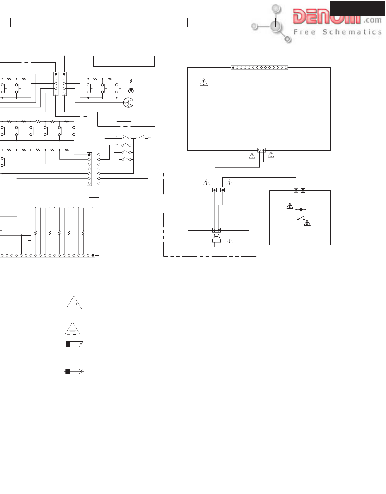
CAUTION
FOR CONTINUED PROTECTION
AGAINST FIRE HAZARD, REPLACE
ONLY WITH FUSE OF SAME TYPE
VA
AND RATING INDICATED.
ATTENTION
AFIN D'ASSURER UNE PROTECTION
PERMANENTE CONTRE LES RISQUES
D'INCENDIE, REMPLACER UNIQUEMENT
VA
PAR UN FUSIBLE DE MEME TYPE
ET CALIBRATION COMME INDIQUE.
THIS SYMBOL LOCATED NEAR THE FUSE INDICATES
THAT THE FUSE USED IS SLOW OPERATING TYPE
FOR CONTINUED PROTECTION AGAINST FIRE
HAZARD,REPLACE WITH SAME TYPE FUSE. FOR FUSE
RATING REFER TO THE MARKING ADJACENT TO THE SYMBOL.
CE SYMBOLE INDIQUE QUE LE FUSIBLE UTLISE EST
E LENT.POUR UNE PROTECTION PERMANENTE,N'UTILISER
QUE DES FUSIBLES DE MEME TYPE. CE DARNIER EST
INDIQUE LA QU LE PRESENT SYMBOL EST APPOSE.
S723
S722
STANDBY
Q721
RN1407
ENTER
S731
NPS-115-S673
D721
STANDBY
Jog Switch
To P902 (Output terminal PC board)
CN2
U10:POWER SUPPLY UNIT
24150020
U9:AC inlet terminal
PC board
P982A (BROWN) P982B (WHITE)
P981B
P981
NAPS-7184
CN1
P982A (BROWN)
P982B (BROWN)
C991
S991
NASW-7186
U6:Power switch
PC board
www.denom.com
Page 17

A
BCDEFGH
SCHEMATIC DIAGRAM
U2:Display circuit PC board
1
2
3
NADIS-7182A
1K
R725
R727R726
Destination
MDD1N
192_L K2
96_L INIT1
PLY_L SYSOUT
STP_L VCOFF
OPC_L LT1
R785
P15 PON
P14 XRDY
P13 SO
P12 SI
P11 XSCK
P10
P9
P8
P7
R721R720
10K 56K
R790
10K
R789
10K
K0
24
25
+5V
VDD0
K1
21
23
K022K1
K2
VSS0
INIT1
GND2
VCOFF
LT1
IRIN
NC2
NC1
SYSRESET
PON
XRDY
SO
SI
XSCK
RESET
GND1
X1
X2
VSS1
VDD1
1G802G793G784G775G766G757G748G
VOF_L
STB_L
MSO_0
MSO_1
MSO_2
FL_ON/OFF ENTER
39
40
VLED
192LED
41
42
43
44
45
46
47
48
49
50
51
52
53
54
55
56
57
58
59
60
96LED
PLYLED
STPLED
OPCLED
LEDO
NC5
NC6
NC7
P15
P14
P13
P12
P11
P10
P9
P8
P7
VDD2
VLOAD
61
P6P5P4P3P2
MSO_038MSO_137MSO_2
STBYLED
232SO
34
NC3
R759
R713
0
0
33
TEST
232SI
232SCK
R712
R7110
0
31
32
R232SO
R232SCK
SRESET
36
35
NC4
Q701
MPD780232GC
12G6913G6814G
P1
P265P364P463P562P6
66
P1
14G
70
67
13G
12G
11G
10G
232BU
232RE
SYSIN
SYSOUT
R788
10K
R709
R710
0
0
29
28
30
26
27
SYSIN
R232SI
SYSOUT
R232REQ
R232BUSY
10G7111G
9G
73
72
9G8G7G6G5G4G3G2G1G
0
MSO_0
20
19
18
17
16
15
14
13
12
11
10
9
8
7
6
5
4
3
2
1
MSO_1
C702
0
104Z
R724
MSO_2
R708
R707
R706
R705
R704
R703
R702 0
C701
R722 R723
INIT1
0
0
0
0
0
0
100/6.3
REMO
RESET
R701
R721R720
1M
R786 R787
SYSIN
X701
2.7K
R719
K0K1K2
5.00MHZ
10K
2.7K
2.7K
R717
R718
47K
Q704
RN2403
C706
223Z
R782
Q705
Remote
Sensor
REMO
D701
1SS352
P710A
R714
4.7K
Q703
BMR-0101D
O
I
G
C704
100/6.3
R716 220KR715
D702
UDZS5.6B
RI
C703
22/50
K0
STB_L
VOF_L
K1
K2
R747
390
S712
CLEAR
R733
390
S701
T.MENU
R740
390
S709
PAUSE
R751
232RE
RANDOM
MENU
STOP
R752
232BU
R748
470
S713
REPEAT
R734
470
S702
SETUP
R741
470
PLAY
S710
R753
232SI
SRESET
21
22
NC
SRESET
R749
820
R735
820
R742
820
FLAC2
FLAC1
20
FLAC2
Q706
BD4742G
Q723
2S
FL_ON/OFF
P15
P14
P13
P9P8P7P6P5P4P3P2P1
P12
P11
P10
14G
13G
12G
9G8G7G6G5G4G3G
11G
10G
1G
2G
NC
24531
4
0
R781
R552
2S
Q724
R780
F1 48
P13 42
P14 43
P15 44
38
P9
P10 39
P11 40
P12 41
P5 34
P6 35
P7 36
P8 37
P1 30
P2 31
P3 32
P4 33
Q702
14G18
FL tube
9G 13
10G14
11G15
12G16
13G17
5G 9
6G 10
7G 11
8G 12
1G 5
2G 6
3G 7
4G 8
F2' 1
NOTE
.
THE COMPONENTS IDENTIFIED
REPLACE ONLY
.
VOLTAGE (MEASURED WITHVOLTMETER) IS
.
ELECTROLYTIC CAPACITORS (
.
5
ALL CAPACITORS ARE IN pF/50WV UNLESS OTHERWISE NOTED.
EX) 030 3pF 330 33pF 331 330pF
.
ALL RESISTORS ARE IN OHMS 1/4WATTS
.
THE THICK LINES ON PC BOARD ARE THE PRINTING SIDE OF THE PARTS.
EX) PRINTING SIDE
.
CIRCUIT IS SUBJECT TO CHANGE FOR IMPROVEMENT.
WITH PART
MARKBY
NUMBER SPECIFIED.
ARE CRITICAL FOR SAFETY.
ARE IN F/WV.
)
333 0.033uF
DCVOLTAGE.
u
UNLESS OTHERWISE NOTED.
(NO INPUT SIGNAL)
www.denom.com
Page 18
R749
820
S714
REPEAT
R735
820
S703
SETUP
R742
820
PLAY
S711
R750
1K
S715
MEMORY
R736
1K
S704
RETURN
R743
1K
R737
1.8K
S705
DISPLAY
R744
1.8K
R738
3.9K
DOWN
R745
3.9K
U3:Standby LED PC board
NADIS-7183A
R771
R772
1.8K
3.9K
R773
JL771A
UP
S706
JL771B
R739
10K
S707
R746
10K
OPEN
S708
DOWN
UP
RIGHT
LEFT
V_OFF
P731
S721
DIMMER
7
6
5
4
3
2
1
S723
S722
D721
STANDBY
ENTER
STANDBY
Q721
RN1407
S731
NPS-115-S673
Jog Switch
U9:AC inlet terminal
PC board
To P902 (Output terminal PC board)
CN2
U10:POWER SUPPLY UNIT
24150020
P982A (BROWN) P982B (WHITE)
CN1
P982A (BROWN)
DPS-5.2
P982B (BROWN)
RI
LT1
VCOFF
R754
GND
E+5V
18
-27V
VCOFF
17
15
E+5V
GND116GND2
VCOFF
GND
LT1_1RIRESET
14
-27V
FLAC2
FLAC1
19
20
FLAC1
FLAC2
To Out put terminal PC board
13
LT1
100
RESET
232RE
R755
232RE_1
10
11RI12
RESET
PON
XRDY
232BU
100
100
R756
PON
XRDY
232BU_1
9
7
8
PON
XRDY
232BU
232RE
THIS SYMBOL LOCATED NEAR THE FUSE INDICATES
THAT THE FUSE USED IS SLOW OPERATING TYPE
FOR CONTINUED PROTECTION AGAINST FIRE
HAZARD,REPLACE WITH SAME TYPE FUSE. FOR FUSE
RATING REFER TO THE MARKING ADJACENT TO THE SYMBOL.
CE SYMBOLE INDIQUE QUE LE FUSIBLE UTLISE EST
E LENT.POUR UNE PROTECTION PERMANENTE,N'UTILISER
QUE DES FUSIBLES DE MEME TYPE. CE DARNIER EST
INDIQUE LA QU LE PRESENT SYMBOL EST APPOSE.
SO
SI
232SCK
R758
SI_1
232SCK
4
232SCK
232SO
100
232SO
2
232SO
XSCK
XSCK
1SI3SO5
SCK
P701B
232SI
100
R757
232SI_1
6
232SI
SO
CAUTION
FOR CONTINUED PROTECTION
AGAINST FIRE HAZARD, REPLACE
ONLY WITH FUSE OF SAME TYPE
VA
AND RATING INDICATED.
ATTENTION
AFIN D'ASSURER UNE PROTECTION
PERMANENTE CONTRE LES RISQUES
D'INCENDIE, REMPLACER UNIQUEMENT
VA
PAR UN FUSIBLE DE MEME TYPE
ET CALIBRATION COMME INDIQUE.
NAPS-7184
P981B
P981
C991
S991
NASW-7186
U6:Power switch
PC board
www.denom.com
Page 19

DP-S5.2
A
SCHEMATIC DIAGRAM
1
2
3
U7: RS-232C connector PC board
NAETC-7188
RXD15
TXD16
BCDEFGH
PRINTED CIRCUIT BOARD VIEWS
NAETC-7188
RESET
J804
VPP
P802
GND
+5V
7
J801
C813
HS
VPP
VDD
RST
SCK
SO
SI
GND
Not used
REQ
SCK
BUSY
SDATAIN
0
0
0
R802
R804
R803
NC12
SI 10
REQ13
SCK11
BUSY14
MPD789071MC
PORT117
PORT319PORT420PORT521PORT622PORT723PORT824PORT925
PORT2
18
P802 P751B
X801
5.00MHZ
SDATAOUT
0
0
R806
R805
SO 9
X1 6
VDD 8
VSS 7
Q801
To Output terminal PC board
SCK
REQ
SDATAOUT
C810
R808
PORT14
30 PORT15 1
BUSY
SDATAIN
100/6.3
C811
104Z
EVER+5V
R801
1M
RESET
47
R807
5
IC 3
X2
RESET 4
PORT10
PORT11
PORT12
26
27
28
RESET
2
PORT16
PORT13
29
GND
U7: RS-232C connector PC board
J808
RESET
P801
P751B
P801
C801
NCETC-7188
25137188
C804
Component side view
J806
J807
C810
C802
1
C803
+5V
GND
X801
1
+5V
7
J803
J805
7
J802
1/50
C802
1/50
C803
C812
L801
BK1608LM182-T
104Z
C813
100/6.3
C812
L801
R810
R808
R809
R811
R807
C811
Q802
Q802
1
R806
Q801
Q801
R805
R804
R802
L802
L804
L803
L805
R803
R812
RXD_FL
TXD_FL
RTS_FL
47
R812
47
R811
47
R809
CTS_FL
C801
5
6
7
8
9
1011
Q802 MPD4721GS
12131415161718
C804
4
1/50
3
1/50
2
19
1
20
47
R810
4
5
NAETC-7188
L802
L803
BK1608LM182-T
BK1608LM182-T
BK1608LM182-T
L804
L805
BK1608LM182-T
P801
RS-232C CONNECTOR
(9PIN D-SUB CONNECTOR)
Soldering side view
www.denom.com
Page 20

A
BCDEFGH
SCHEMATIC DIAGRAM
1
U7: RS-232C connector PC board
NAETC-7188
Not used
P802 P751B
X801
5.00MHZ
To Output terminal PC board
SCK
REQ
SDATAOUT
BUSY
SDATAIN
R801
1M
RESET
2
REQ
SCK
BUSY
SDATAIN
SDATAOUT
0
0
0
0
0
R802
R806
R805
R804
R803
NC12
SI 10
REQ13
RXD15
BUSY14
3
MPD789071MC
PORT117
TXD16
PORT2
18
SO 9
SCK11
VDD 8
Q801
PORT319PORT420PORT521PORT622PORT723PORT824PORT925
VSS 7
5
X1 6
X2
PORT10
26
RESET
47
R807
IC 3
RESET 4
PORT11
PORT12
27
28
C810
R808
2
PORT16
PORT13
PORT14
29
30 PORT15 1
100/6.3
C811
104Z
EVER+5V
GND
1/50
C802
1/50
C803
C812
L801
BK1608LM182-T
104Z
C813
100/6.3
RXD_FL
TXD_FL
RTS_FL
47
R812
47
R811
47
R809
CTS_FL
C801
5
6
7
8
9
1011
Q802 MPD4721GS
12131415161718
C804
4
1/50
3
1/50
2
19
1
20
47
R810
4
5
NAETC-7188
L802
L803
BK1608LM182-T
BK1608LM182-T
L804
BK1608LM182-T
www.denom.com
BK1608LM182-T
L805
P801
RS-232C CONNECTOR
(9PIN D-SUB CONNECTOR)
Page 21

DP-S5.2
10
To Spindle motor
A
BCDEFGH
SCHEMATIC DIAGRAM (Page 1)
Main circuit PC board
1
(RF)
: RF SIGNAL ROUTE
(V)
15p
82k
10k
22k
Page 3
Page 2
0.01
TC7SZU04F
IC304
470
100k
1k
3.3k
(V) (V)
Page 2
Page 3
Page 2
(V) (V)
2
(RF)
(RF)
Page 2
(F)
(T)
(T)
(V)
(V)
(A)
(F)
(A)
(F)
(T)
(A)
(F)
(T)
(V)
: RF (VIDEO) SIGNAL ROUTE
(A)
: RF (AUDIO) SIGNAL ROUTE
(AD)
: AUDIO DATA SIGNAL ROUTE
(F)
: FOCUS SERVO LOOP LINE
(T)
: TRACKING SERVO LOOP LINE
(S)
: SLIDER SERVO LOOP LINE
V+5V
3V to 5Volt
Q171
RN4982-TLB
(UMD3N)
5
DF OUT
From DSP IC
54p
6
2
1
4
3
Page 1
to RF IC (IC 101)
28p
3
(AD)
CN151
(RF)
4
(F)
(F)
PICKUP ASSY
(T)
(T)
(F)
(F)
Page 2
(F)
(T)
(T)
(F)
(S)
(S)
(T)
(F)
(A)
(F)
(T)
Page 2
FR CPU
To Q171
Page 3
BY CHIP
(T)
(F)
5
(A)
(F)
(T)
7
Page 2
From FR CPU
8 9
Page 3
111110
CN601
To Spindle motor
5
CN52
Load PCB
For Mecha
connector
(F)
(T)
(T)
(F)
(F)
(T)
(T)
(F)
(F)
(F)
(T)
(T)
Page 2
FR CHIP (IC601)
Page 3
BY CHIP (IC701)
162p
Page 3
www.denom.com
Page 22

A
To Spindle motor
BCDEFGH
SCHEMATIC DIAGRAM (Page 1)
Main circuit PC board
1
Page 2
Page 2
(V) (V)
2
(RF)
(RF)
Page 2
(F)
(T)
(T)
(V)
(V)
(A)
(F)
(A)
(F)
(T)
(A)
(F)
(T)
3
CN151
(RF)
4
(F)
(F)
PICKUP ASSY
CN601
5
CN52
Load PCB
For Mecha
connector
(T)
(T)
(F)
(F)
Page 2
(F)
(T)
(T)
(F)
(F)
(F)
(S)
(S)
To Spindle motor
(T)
(T)
(F)
(F)
(T)
(T)
(F)
(F)
(T)
(T)
www.denom.com
Page 23

DP-S5.2
10
(RF)
: RF SIGNAL ROUTE
(V)
82k
15p
10k
22k
Page 3
0.01
TC7SZU04F
IC304
470
100k
1k
3.3k
(V)
Page 3
(V) (V)
Page 2
: RF (VIDEO) SIGNAL ROUTE
(A)
: RF (AUDIO) SIGNAL ROUTE
(AD)
: AUDIO DATA SIGNAL ROUTE
(F)
: FOCUS SERVO LOOP LINE
(T)
: TRACKING SERVO LOOP LINE
(S)
: SLIDER SERVO LOOP LINE
V+5V
3V to 5Volt
Q171
RN4982-TLB
(UMD3N)
5
DF OUT
From DSP IC
54p
6
2
1
4
3
Page 1
to RF IC (IC 101)
28p
Page 2
(AD)
From FR CPU
Page 3
(T)
(F)
(A)
(T)
(F)
5
(A)
Page 2
FR CPU
(F)
(T)
Page 3
BY CHIP
(F)
(T)
8 9
To Q171
7
Page 2
FR CHIP (IC601)
Page 3
BY CHIP (IC701)
162p
Page 3
111110
www.denom.com
Page 24

DP-S5.2
A
SCHEMATIC DIAGRAM (Page 2)
1
2
BCDEFGH
VYW1853
CLOCK GENERATOR
R489
Page 1
22
Page 1
Page 3
Page 1
Page3
Page3
Page 1
3
470k
4
CN512
MECHA
Page1
page 4
To CN15
(D)
: AUDIO (DIGITAL) SIGNAL ROUTE
CN401
1
2
3
4
5
6
7
8
9
10
11
12
13
14
15
16
17
18
19
20
21
22
23
24
(D)
25
(D)
26
27
28
29
30
(D)
To Output terminal PC board
CN102
5
To CN15
Page 4
Video encoder
IC861 45p
page 4
page 1 IC201
: The power supply is shown with the marked box.
www.denom.com
Page 25

A
SCHEMATIC DIAGRAM (Page 2)
1
BCDEFGH
VYW1853
Page 3
2
Page 1
Page 1
Page 1
Page3
Page3
3
470k
page 4
To CN15
4
CN512
MECHA
Page1
5
To CN15
Page 4
Video encoder
IC861 45p
page 4
page 1 IC201
www.denom.com
Page 26

CLOCK GENERATOR
R489
DP-S5.2
Page 1
22
(D)
: AUDIO (DIGITAL) SIGNAL ROUTE
(D)
(D)
(D)
: The power supply is shown with the marked box.
CN401
2
4
6
8
10
12
14
16
18
20
22
24
26
28
30
1
3
5
7
9
11
13
15
17
19
21
23
25
27
29
To Output terminal PC board
CN102
www.denom.com
Page 27

SCHEMATIC DIAGRAM (Page 3)
DV-S555
(VD)
***
C742
C705
***
(VD)
(V)
220/4
IC712
4M MSM51V17805D-60TS (SOP)
To SCRUT 7,21, 68, 188P
to CN15 page 4
Page 1 IC201
Page 1
R334
to CN401
Page 2/ IC601
Page 2/ IC601
Page 2/ IC601
Page 3 IC 801
Page 1 IC 201
(AD)
(AD)
www.denom.com
Page 2 IC 601
(V)(V)
Page 1
to Page 1
Page 28

SCHEMATIC DIAGRAM (Page 3)
PAL model only
IC806
(V)
: RF (VIDEO) SIGNAL ROUTE
(VD)
: VIDEO DATA SIGNAL ROUTE
(AD)
: AUDIO DATASIGNAL ROUTE
: AUDIO SIGNAL ROUTE
(D)
: AUDIO (DIGITAL) SIGNAL ROUTE
DV-S555
(VD)
from AV1 88p IC801
(VD) (VD)
DCS2
Page 2
IC801
(VD)
(D)
(D)
from Clock generator Page 2
MAIN/ADDRESS/DATA from FR30 Page 2 IC601
www.denom.com
from Clock generator Page 2
from SCRUT Page 3 IC701
Page 2 IC601
Page 29

DP-S5.2
A
SCHEMATIC DIAGRAM (Page 4)
1
2
BCDEFGH
(VD)
: VIDEO DATASIGNAL ROUTE
(V)
: V SIGNAL ROUTE
(Y)
: Y SIGNAL ROUTE
(C)
: C SIGNAL ROUTE
(R)
: R SIGNAL ROUTE
(G)
: G SIGNAL ROUTE
(B)
: B SIGNAL ROUTE
: AUDIO SIGNAL ROUTE
3
(V) (V) (V)
Page 2
FR CPU 101p
from AV 1 MPEG decoder
(IC801)
page 3
(V)
4
(VD) (VD)
5
(Y)
(C)
(V)
(Y)
(C)
(R)
(B)
(Y)
(C) (C)
(Y)
(G)(G)
(Y) (Y)
(C)
(R)(R)
(G)
(B)(B)
(G)
(V)
(V)
(R)
(R)
(G)
page 2
FR CPU
page 3
(Y)
(R)
(C)
(G)
(V)
(B)
(B)
(R)
(G)
(Y)
(C)
(V)
(B)
CN15
CN106
Page 2
www.denom.com
Page 30

A
SCHEMATIC DIAGRAM (Page 4)
1
2
BCDEFGH
3
(V) (V) (V)
Page 2
FR CPU 101p
from AV 1 MPEG decoder
(IC801)
page 3
(V)
4
(VD) (VD)
5
(Y)
(C)
(V)
(Y)
(C)
(R)
(B)
(Y)
(C) (C)
(Y)
(G)(G)
Page 2
www.denom.com
Page 31
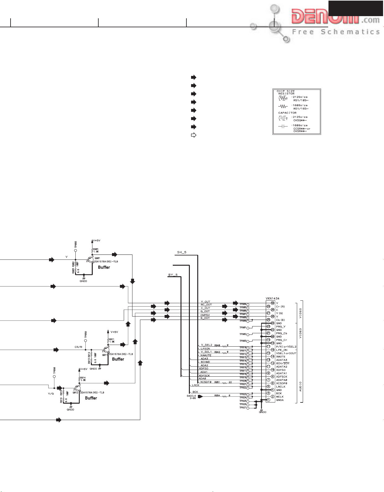
(VD)
: VIDEO DATASIGNAL ROUTE
(V)
: V SIGNAL ROUTE
(Y)
: Y SIGNAL ROUTE
(C)
: C SIGNAL ROUTE
(R)
: R SIGNAL ROUTE
(G)
: G SIGNAL ROUTE
(B)
: B SIGNAL ROUTE
: AUDIO SIGNAL ROUTE
DP-S5.2
(V)
(Y) (Y)
(C)
(R)(R)
(G)
(G)
(B)(B)
page 2
FR CPU
(V)
(R)
(R)
(G)
page 3
(Y)
(R)
(C)
(G)
(V)
(B)
(B)
(R)
(G)
(Y)
(C)
(V)
(B)
CN15
CN106
www.denom.com
Page 32

PRINTED CIRCUIT BOARD PARTS LIST
Output terminal PC board (NAAR-7181-1G)
CIRCUIT NO. PART NO. DESCRIPTION CIRCUIT NO. PART NO. DESCRIPTION
ICs Socket AS
Q201
Q301
Q351
Q401,Q402
Q901
Q902
Q202,Q204, 2216340R2 or
Q303,Q410
Q203,Q205 2216230R2 or
Q403-Q405
Q412
Q352
D402
D901
L201-L206,
L351-L353
C201,C409, 354741019 100uF, 16V, Elect.
C410,C912,
C911
C210 354741009 10uF, 16V, Elect.
C215,C913 354744709 47uF, 16V, Elect.
C217,C218, 354724719 470uF, 6.3V, Elect.
C221,C222
C220 354721029 1000uF, 6.3V, Elect.
C301,C303, 354721019 100uF, 6.3V, Elect.
C305,C353,
C358
C401,C402, 354782209 22uF, 50V, Elect.
C411,C412,
C415
C902,C904, 354742219 220uF, 16V, Elect.
C906
C908,C910 354722219 220uF, 6.3V, Elect.
CN102,CN106 25052610
P104
P751A 25052308 or
22241623R2
22241617R2
22274004HR2O
22240581R2 or
22241383R2 NJM4565M-D
222780085
22241515R2
Transistors
2216260R2
2214540R2
2216141R2
2214373R2 or
2214374R2 or
2216183R2 or
2216184R2 or
2216185R2
Photo coupler
24120093
Diodes
223234R2 or
223269R2
224550510R2
Coils
230958R1
Capacitors
Sockets
or
25052344
25051889 or
25052528
25052502
25052502
MM1540BF
PCM-1742KE
TC74VHCU04FT
NJM4565M or
78M08HF
PQ025EZ5MZP
KRC107S or
RN1407
KRA103S or
RN2403
HN1C03F-B
2SA1162-O or
2SA1162-Y or
KTA1504-O or
KTA1504-Y or
KTA1504-GR
JFJ3000
1SS352 or
1SS355
UDZS5.1B, Zener
BK1608LM182-T
NSCT-30P-2507
NSCT-7P2241 or
NSCT-7P1676 or
NSCT-7P2425
NSCT-8P2205 or
NSCT-8P2399 or
NSCT-8P2399
P351A 200BB190415UL
P902
P201
P203
P353
P354
P401
P402
Display circuit PC board (NADIS-7182-1G)
CIRCUIT NO. PART NO. DESCRIPTION
Q701
Q706
Q702A 212219
Q704
Q705
X701
D701 223234R2 or
D702
JL771A 25051089
P701A 25052322 or
P701B 25052359 or
P731 25052344 or
C701,C704
C703 355782209 22uF,50V,Elect
S701-S715
Q702B 27191141
2002A392815
Jacks
25045658
25045661
25045592
25045330 or
25045481
25045662
25045593
ICs
22241727R3
22241713R2
FL tube
Transistors
2216230R2 or
2214540R2
Remote senso
241336
241329
Resonator
3010242
Diodes
223269R2
224550560R2
Sockets
25051946 or
25052516
25051904
25052543
25051889 or
25052528
Capacitors
355721019 100uF,6.3V,Elect
Switches
25035699
FL holder
NSAS-4P0816
NSAS-28P0742
NPJ-5PDBY457, S-Video
NPJ-3PDGLR460,
Com
ponent
NPJ-1PDOR403, Coaxial
NPJ-2PDBL184 or
NPJ-2PDBL299, RI
NPJ-3PDBRW461,
Analo
g out 3P
NPJ-2PDWR404,
Analog out 2P
MPD780232GC-045-8BT
BD4742G
14-BT-68GNK
KRA103S or
RN2403
r
PIC-37043TH2 or
PIC-26043TH2
CST5.00MGW
1SS3522 or
1SS355
UDZS5.6B, Zener
NSCT-5P876
NSCT-22P2219 or
NSCT-22P1733 or
NSCT-22P2413
NSCT-22P2256 or
or
NSCT-22P1691 or
NSCT-22P2440
NSCT-7P2241 or
NSCT-7P1676 or
NSCT-7P2425
NPS-111-S662
DPS-5.2
www.denom.com
Page 33

PRINTED CIRCUIT BOARD PARTS LIST
N
N
N
N
Standby LED PC board (NADIS-7183-1G) RS-232C connector PC board (NAETC-7188-1G)
CIRCUIT NO. PART NO. DESCRIPTIO
Transistor ICs
Q721
D721
S723
Inlet terminal PC board (NAPS-7184-1G) C810,C813 354721019 100uF,6.3V, Elect.
CIRCUIT NO. PART NO. DESCRIPTIO
P981B 25055960
P982A 2069943301UL P801
P982B 2009990661UL
Power switch PC board (NAPS-7186-1G)
CIRCUIT NO. PART NO. DESCRIPTIO
S991 25035703
C991 3500196S
2216340R2 or
2216260R2
LED Resonator
225290
Switch Filters
25035699
Terminal P751B 25052308 or
Socket AS 25052502
Switch
25035550
Capacitor
KRC107S or
RN1407
SEL4110R
NPS-111-S662,
STANDBY
NPLG-2P913, AC inlet
NSAS-2P0921
NPS-111-L666P or
NPS-111-L512P
RE275V-103M, ISC
CIRCUIT NO. PART NO. DESCRIPTIO
Q801
Q802
X801
L801-L805
C801-C804
NOTE: THE COMPONENTS IDENTIFIED BY MARK
ARE CRITICAL FOR RISK OF FIRE AND
ELECTRIC SHOCK. REPLACE ONLY WITH
PART NUMBER SPECIFIED.
22241624R2
22241537R2
3010242
230958R1
Capacitors
354780109
Sockets
25052502 or
25052379
MPD789071MC-011-5A4
MPD4721GS
CST5.00MGW
BK1608LM182-T
1uF,50V, Elect.
NSCT-8P2205 or
NSCT-8P2399 or
NSCT-8P2399
NSCT-9P2277
DPS-5.2
www.denom.com
Page 34

Disassembly of the Traverse Mechanism Assy
DPS-5.2
Remove the top cover and Tray Panel.
1
Remove the Tray panel and Front Panel.
2
Remove the Bridge (Screw 1).
3
Pull out the Tray and remove it while unhooking a Hook.
4
Turn the Short SW to Short side.
5
Remove three connectors.
6
-1
4
Hook
Bridge
-2
3
-1
3
6
6
6
-2
4
DVD main PC board assy
RearView
Remove the Loading Mechanism Assy (Screws 4).
7
Remove a screw.
8
Cautions:
Screw is locked with Silicone Adhesive.
Please lock it with Silicone Adhesive when installs it.
Remove the FFC Holder with the state which Flexible Cable
9
was attached.
8
Traverse Mechanism
Assy
Silicone Adhesive
GEM1037
9
FFC
Holder
Bottom View
DVD main
PCB side
Short
Open
5
Short SW
Caution in the tray insertion
In the Tray insertion, insert it after matching a triangle mark
of the Loading Base and a position of pin of the Drive Cam.
Triangle mark
Loading Base
Drive CamPin
When Removing The Traverse Mechanism Assy
Remove the Pickup Flexible Cable
10
Unhook ( 4)
11
Remove the Traverse Mechanism Assy
12
11
2
12
10
2
11
Exchange
Traverse Mechanism
Assy
www.denom.com
Page 35

PC BO ARD CONNECTION DIAGRAM
NAPS-7184
U9: Inlet terminal
BRN
P982A
BRN
BRN
WHT
CN1
U10: Power supply
PC board
NGPS-0020/0021
WHT
P982B
PC board
Z10: Main circuit PC board
CN52
CN401
To CN102
IC601
Pickup
CN120
IC701
IC712
DB-VPB301
IC201
IC801
IC805
DPS-5.2
U7: RC-232C connector
PC board
P104
NC
TXD
CTS
DTR
RXD
V+5D
GND
P902
+3.3V
GND
SW+5V
GND
V+12V
MGND
M+5V
GND
EVER+5V
P ON
FLAC2
FLAC1
-27V
GNDD
P351A
CN251CN3
IC351
CN15
To CN106
SQUEEZE
P250A
V+12V
VSEL1
C
VSEL2
Y
GNDV1
V
GNDV2
G
GNDV3
B
GNDV4
R
GNDV5
+5V
AUDIO L
GNDA
AUDIO R
V+8V
U1: Output terminal
PC board
GND
DOUT
P351A
NAAR-7181
NAETC-7188
P751B
P751A
GND
+3.3V
GND
CN2
SW+5V
GND
V+12V
MGND
M+5V
GND
EVER+5V
P ON
FLAC2
FLAC1
-27V
NASW-7186
P982CP982D
U6: Power switch
PC board
DVD mechanism
CN601
U3:Standby LED
PC board
NADIS-7183
Standby
JL771A
JL771B
CN102
U2: Display circuit PC board
NADIS-7182
CN106
Cursor button
P711
P710B
(Jog dial)
P701B
RESET
GND
P710
P731
-
Left
GND
Right
EnterUpDown
7
22
SRESET
P701B
SI
RI
NC
-27V
FLAC2
FLAC1
SO
LT1
E+5V
GND1
GND2
VCOFF
SCK
PON
232SI
XRDY
232BU
232RE
232SO
RESET
232SCK
www.denom.com
Page 36

FL TUBE VIEW
DTS
GUI
5.1ch
DVD-AUDIO
VCD
PBC3D3D
PAL
RANDOM
MEMORY
ALL
REPEAT
1A-B
CHAPTER
TRACK
TEXT
TOTAL
REMAIN
DISC
TITLE
GROUP
LS
RS
LFE
LAST
D.MIX
COND.
DTS
GUI
5.1ch
COND.
LAST
D.MIX
LFE
RS
LS
RANDOM
MEMORY
ALL
REPEAT
TEXT
TRACK
TOTAL
CHAPTER
REMAIN
DVD
AUDIO
DISC
CD
TITLE
PBC
3D
GROUP
PAL
Pin connection
DPS-5.2
DVD-A UDIO
DISC
D
DTS
GUI
5.1ch
484746454443424140393837363534333231302928272625242322212019181716151413121110987654321
F2NXNPNPP15P14P13P12P11P10P9P8P7P6P5P4P3P2P1NXNXNXNXNXNXNXNXNXNXN
ANODE CONNECTION
3G
a
h
k
b
m
g
c
e
r
p
n
d
a
h
j
j
k
b
f
f
m
g
c
e
e
p
n
d
co
P1
P2
P3
P4
P5
P6
P7
P8
P9
P10
P11
P12
P13
P14
P15
1G
a
h
k
b
m
g
c
e
p
n
d
2G
l
f
r
11G
VCD
TITLE
PBC
PAL
GROUP
9G 8G 7G
a
f
g
e
d
5G
4G
a
h
j
k
b
f
m
m
g
c
e
r
p
n
d
co
[ 14G ]
a
h
j
k
b
f
g
c
e
r
p
n
d
RANDOM
CHAPTER
b
c
6G
a
h
j
k
b
f
m
g
c
e
r
p
n
d
12G
MEMORY
ALL
TRACK
REPEAT
TEXT
TOTAL
6G 5G 4G 3G
h
f
g
r
e
d
7G
a
h
j
k
b
f
m
g
c
e
r
p
n
d
REMAIN
a
j
b
k
col
m
n
c
p
[ 10G - 1G]
X14G13G12G11G10G9G8G7G6G5G4G3G2G1GNPNPNX
8G
a
h
j
k
b
f
m
g
c
e
r
p
n
d
1A-B
[5G,3G]
9G
13G
L C
R
LFE
LAST
D.MIX
11G 12G
PAL
j
3D
GROUP
PBC
TITLE
CD
V
DISC
-
AUDIO
DVD
COND.
1G2G14G 10G
RANDOM
MEMORY
ALL
REPEAT
1
A
-
B
TEXT
TRACK
CHAPTER
TOTAL
REMAIN
F
1
13G 14G
L
C
R
LS
S
RS
LFE
D.MIX
LAST
COND.
a
D
DTS
GUI
b
f
5.1ch
g
c
e
d
SLS
RS
10G
a
h
a
h
j
k
b
f
m
g
c
e
r
p
n
d
k
b
f
m
g
c
e
r
p
n
d
www.denom.com
Page 37

MICROPROCESSOE TERMINAL DESCRIPTION
MPD780232GC-041-8BT
Pin No. Symbol Function I/O Description Pin No. Symbol Function I/O Description
1 Vdd1
2 Vss1
3X2 X
4X1 X
5IC
6 ~RESET
7 P27/~SCK1
8 P26/SI1
9 P25/SO1
10 P24/BUSY
11 P23
12 P22
13
P21/SO3 Not used 53 P31/FIP25 P12 O FL segment (P12) control output pin
P20/~SCK3 Not used 54 P30/FIP24 P11 O FL segment (P11) control output pin
14
15 P00/INTP0
16 P01/INTP1
17 P02/TI
18 AVss
19 ANI3
20 ANI2
21 ANI1
22 ANI0
23 Vss0
24 AVdd
25 Vdd0
26 P64/FIP52
27 P63/FIP51
28 P62/FIP50 R232REQ I REQ input pin from microprocessor of RS-232C driver 68 FIP12
29 P61/FIP49 R232BUSY I BUSY input pin from microprocessor of RS-232C driver 69 FIP11
30 P60/FIP48 R232SI I SI input pin from microprocessor of RS-232C driver 70 FIP10
31 P57/FIP47 R232SCK O SCK input pin from microprocessor of RS-232C driver 71 FIP9
32 P56/FIP46 R232SO O SO input pin from microprocessor of RS-232C driver 72 FIP8
33 P55/FIP45 TEST I Testing pin 73 FIP7
34 P54/FIP44
35 P53/FIP43
36 P52/FIP42 MS0_2 I Model select input pin 2 76 FIP4
37 P51/FIP41 MS0_1 I Model select input pin 1 77 FIP3
38 P50/FIP40 MS0_0 I Model select input pin 0 78 FIP2
39 P47/FIP39
40 P46/FIP38
Vdd1 Power supply, +5V 41 P45/FIP37
Vss1 Ground pin 42 P44/FIP36
2 Main clock input pin (5MHz) 43 P43/FIP35
1 Main clock input pin (5MHz) 44 P42/FIP34
GND Ground pin 45 P41/FIP33
RESET Reset pin of microprocessor 46 P40/FIP32
XSCK
SI
SO
XRDY
PON
SYSRESET
~IRIN
LT1
VCOFF
GND Ground pin for D/A converter 58 FIP20 P7 FL segment (P7) control output pin
INIT1 Initializing input pin (Analog signal) 59 Vdd2 Vdd2 Power supply pin (+5V)
K2 Key input pin 60 Vload Vload FIP control pin to connect pull down resistor
K1 Key input pin 61 FIP19 P6 FL segment (P6) control output pin
K0 Key input pin 62 FIP18 P5 FL segment (P5) control output pin
Vss0 Ground pin 63 FIP17 P4 FL segment (P4) control output pin
+5V Power supply pin of D/A converter, +5V 64 FIP16 P3 FL segment (P3) control output pin
Vdd0 Power supply, +5V 65 FIP15 P2 FL segment (P2) control output pin
~SYSIN
~SYSOUT
R232RES
FLON_OFF
STBYLED
VCOFFLED
Clock output pin for writhing of flash ROM 47 P37/FIP31 O Not used
Data input pin for writhing of flash ROM 48 P36/FIP30 O Not used
Data output pin for writhing of flash ROM 49 P35/FIP29 O Not used
XRDY output pin 50 P34/FIP28 P15 O FL segment (P15) control output pin
Power ON control signal output pin (Power ON: "H") 51 P33/FIP27 P14 O FL segment (P14) control output pin
Reset control output pin 52 P32/FIP26 P13 O FL segment (P13) control output pin
Remote control1 signal input pin. 55 FIP23
LT1 data input pin 56 FIP22
Video circuit off control output pin 57 FIP21
I System buss input pin 66 FIP14
O System buss output pin 67 FIP13
O Reset control output pin to microprocessor of RS-232C driver 74 FIP6
O FL filament on/off control output pin 75 FIP5
O Standby LED control output pin 79 FIP1
O Video circuit off LED control output pin 80 FIP0
SMP192LED
SMP96LED
PLYLED
STPLED
OPCLLED
LED0
P10 FL segment (P10) control output pin
P9 FL segment (P9) control output pin
P8 FL segment (P8) control output pin
P1 FL segment (P1) control output pin
14G FL grid (G14) output pin
13G FL grid (G13) output pin
12G FL grid (G12) output pin
11G FL grid (G11) output pin
10G FL grid (G10) output pin
9G FL grid (G9) output pin
8G FL grid (G8) output pin
7G FL grid (G7) output pin
6G FL grid (G6) output pin
5G FL grid (G5) output pin
4G FL grid (G4) output pin
3G FL grid (G3) output pin
2G FL grid (G2) output pin
1G FL grid (G1) output pin
O Sampling rate 192 LED control pin
O Sampling rate 96 LED control pin
O Play LED control output pin
O Stop LED control output pin
O Open/ close LED control pin
O General LED control pin
DPS-5.2
www.denom.com
Page 38

UPGRADE FIRMWARE
1. Data writing for DVD main board
1-1. Writing the F/W data in DVD main board
1-1-1 Set the DVD main board on the unit.
1-1-2 Connect the FFC and Jig between the DVD main board and Personal Computer.
(Using the F/W upgrade Jig board and FFC cable to P104)
1-2-3 Then the power and standby switches are turn on.
1-1-4 Run the data writing program.
EX) Save the program above in C:DPS-5.2 folder. The program name are
B1BK1048.SZ0, Down.bat, down, ok_down.exe, ok_down
Open the DOS window
Key input "cd DPS-5.2" and then push the ENTER key.
Turn thepower switch on and push the STANDBY switch.
Key input the " down b1bk1048.szo" and push ENTER.
Push the ENTER again.
Key input "MO"and ENTER.
Key input "SZL"and ENTER.
The program of a computer running automatically.
<Display of Computer>
000000000000000000000000000
Turn off the power switch, and disconnect the upgrade kit. (Finish)
Space
FW file name .sz0
zero
DPS-5.2
C: DPS-5.2
DPS-5.2
DPS-5.2
MS-DOS prompt
dps-5.2
dps-5.2
www.denom.com
Page 39

UPGRADE FIRMWARE
2. Setting the Region code.
2-1 Turn on the power switch and standby switch is turned on.
2-2 Select a regional code. (Using the remote controller RC-449DV Part number 24140449)
Destination RC-449DV (Slide SW: TV position) Transmission Code Region
MDD1N * *
: automatically chosen
*
UPGRADE JIG
1
DPS-5.2
STOPPA USE
PLAY
DOWN UPFR FF
STEP/SLOW
SEARCH
-
RC
449
FUNCTION M
PROGRAM
DV
+
-
CLEAR
23
1
456
789
+
10
0
RANDOM REPEAT A-B
REMOTE CONTROLLER
TVDVD
RC449DV Remote controller
Parts No. 24140449 (U.S.A
remote controller)
RS-232C cable (D-Sub 9pin to
D-Sub 25pin)
female
male
Upgrade jig Part No. GGF1348
Flexible flat cable Part No. GGD1231
3. Confirm the program
3-1 Press the [SETUP] key.
3-2 Select the "Setup Menu Mode", in the "General" menu.
3-3 Push the [DISPLAY] Button. The Region and FW Version information will appear
on the TV Display.
[SETUP]
Setup Navigator Start
Auto Start Off
[ENTER]
Setup Menu Mode
[DISPLAY]
EX) "Region * / Ver:1.048 / AV:6.0/0.3"
www.denom.com
Page 40

DVS-5.2
Integra Division of
ONKYO CORPORATION
Sales & Product Planning Div. : 2-1, Nisshin-cho, Neyagawa-shi, OSAKA 572-8540, JAPAN
Tel: 072-831-8111 Fax: 072-833-5222 http://www.onkyo.co.jp/
Integra Division of
ONKYO U.S.A. CORPORATION
18 Park Way, Upper Saddle River, N.J. 07458, U.S.A.
Tel: 201-785-2600 Fax: 201-785-2650 E-mail: integra@onkyousa.com http://www.integrahometheater.com
PN 0M3686 D0109 Printed in Japan
www.denom.com
 Loading...