

Page 1
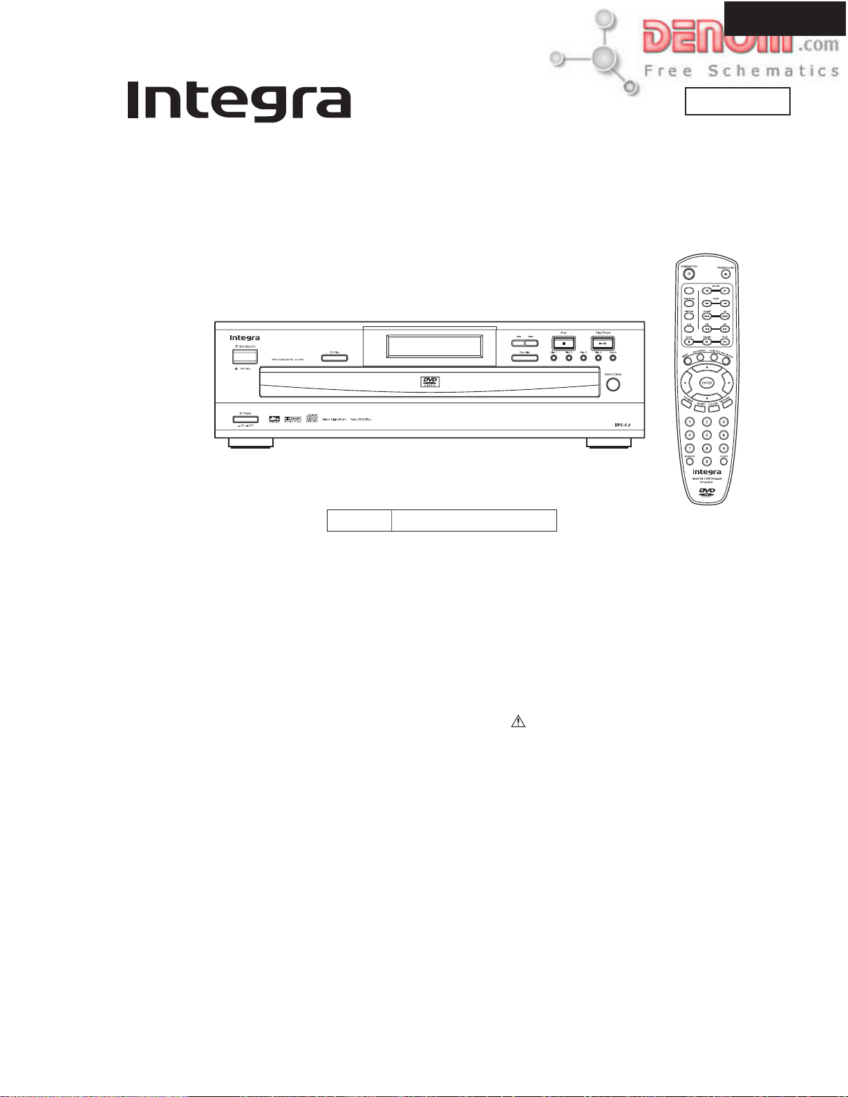
DPC-5.3
SERVICE MANUAL
Ref. No. 3736
SERVICE MANUAL
DVD CHANGER
MODEL DPC-5.3
Black model
120V AC, 60HzBUDD
Sep, 2002
DISC SKIP
RC-503DV
SAFETY-RELATED COMPONENT
WARNING!!
COMPONENTS IDENTIFIED BY MARK ON THE
SCHEMATIC DIAGRAM AND IN THE PARTS LIST ARE
CRITICAL FOR RISK OF FIRE AND ELECTRIC SHOCK.
REPLACE THESE COMPONENTS WITH ONKYO
PARTS WHOSE PART NUMBERS APPEAR AS SHOWN
IN THIS MANUAL.
MAKE LEAKAGE-CURRENT OR RESISTANCE
MEASUREMENTS TO DETERMINE THAT EXPOSED
PARTS ARE ACCEPTABLY INSULATED FROM THE
SUPPLY CIRCUIT BEFORE RETURNING THE
APPLIANCE TO THE CUSTOMER.
www.denom.com
Page 2

SPECIFICATIONS
DVD Changer
Power supply AC 120 V, 60 Hz
Power consumption 20 W
Weight 15.0 lbs
External dimensions 17
Signal system NTSC
Frequency range (digital audio) 48 kHz sampling 4 Hz to 22 kHz
Signal-to-noise ratio (digital audio) More than 98 dB
Audio dynamic range (digital audio) More than 95 dB
1
/8" x 5 1/16" x 16 15/16" (W/H/D)
96 kHz sampling 4 Hz to 42 kHz
DPC-5.3
Harmonic distortion (digital audio) Less than 0.008 %
Wow and flutter Below measurable level
Operating conditions Temperature: 5 C to 35 C (41 F to 95 F)
Operation status: Horizontal
Outputs
V ideo output 1.0 V (p-p), 75 ohm, negative sync., pin jack x 1
S-video output (Y) 1.0V (p-p), 75 ohm , negative sync.
(C) 0.286 V (p-p), 75 ohm , Mini DIN 4-pin x 1
Component video output (Y) 1.0 V (p-p), 75 ohm , negative sync., pin jack x 1
(P
B)/(PR) 0.7 V (p-p), 75 ohm pin jack x 2
Audio output (digital output Optical) Optical connecter x 1
Audio output (digital output Coaxial) 0.5 V (p-p), 75 ohm , pin jack x 1
Audio output (analog output) 2.0 V (r ms), 320 ohm , pin jack (L, R) x 2
Specifications and features are subject to change without notice.
www.denom.com
Page 3
SERVICE PROCEDURE
PRECAUTIONS
1. Ground for the work-desk.
Place a conductive sheet such as a sheet of copper (with impedance lower than 10M ohm) on the work-desk and
place the set on the conductive sheet so that the chassis.
2. Grounding for the test equipments and tools.
Test equipments and toolings should be grounded in order that their ground level is the same the ground of the power source.
3. Grounding for the human body.
Be sure to put on a wrist-strap for grounding whose other end is grounded.
Be particularly careful when the workers wear synthetic fiber clothes, or air is dry.
4. Select a soldering iron that permits no leakage and have the tip of the iron well-grounded.
5. Do not check the laser diode terminals with the probe of a circuit tester or oscilloscope.
DPC-5.3
1. Replacing the fuses
This symbol located near the fuse indicates that the
fuse used is show operating type, For continued protection against
fire hazard, replace with same type fuse , For fuse rating, refer to
the marking adjust to the symbol.
Ce symbole indique que le fusible utilise est e lent.
Pour une protection permanente, n'utiliser que des fusibles de meme
type. Ce demier est indique la qu le present symbol est apposre.
REF.NO.
F1
PART NO.
SR-5, T 2A
DESCRIPTION
250VCA T 2.0A
2. Safety-check out
(Only U.S.A. model)
After correcting the original service problem perform the
following safety check before releasing the set to the customer
Connect the insulating-resistance tester between the plug of
power supply cord and terminal GND on the back panel.
Specifications: More than 10M ohm at 500V
LASER CAUTION
The lightning flash with arrowhead symbol, within an equilateral triangle, is
intended to alert the user to the presence of uninsulated "dangerous voltage"
within the product's enclosure that may be of sufficient magnitude to constitute
a risk of electric shock to persons.
The exclamation point within an equilateral triangle is intended to alert the user
to the presence of important operating and maintenance (servicing) instruction
in the literature accompanying the appliance.
TO REDUCE THE RISK OF FIRE OR ELECTRIC SHOCK, DO NOT EXPOSE THIS APPLIANCE TO RAIN
WARNING :
OR MOISTURE. DANGEROUS HIGH VOLTAGES ARE PRESENT INSIDE THE ENCLOSURE. DO NOT OPEN THE
CABINET. REFER SERVICING TO QUALIFIED PERSONNEL ONLY.
CAUTION :
TO PREVENT ELECTRIC SHOCK, MATCH WIDE BLADE OF PLUG TO WIDE SLOT, FULLY INSERT.
POUR EVITER LES CHOCS ELECTRIQUE, INTRODUIRE LA LAME LA PLUS LARGE DA LA FICHE DANS LA
ATTENTION :
BORNE CORRESPONDANTE DA LA PRISE ET POUSSER JUSQU' AU FOND.
Initialization of setup
1. Press the "CD PLAY" and "DISC 3" key to the same timing on the front panel.
You will see that the program is updated by watching the version in the FL tube.
2. Push the power switch.
www.denom.com
Page 4
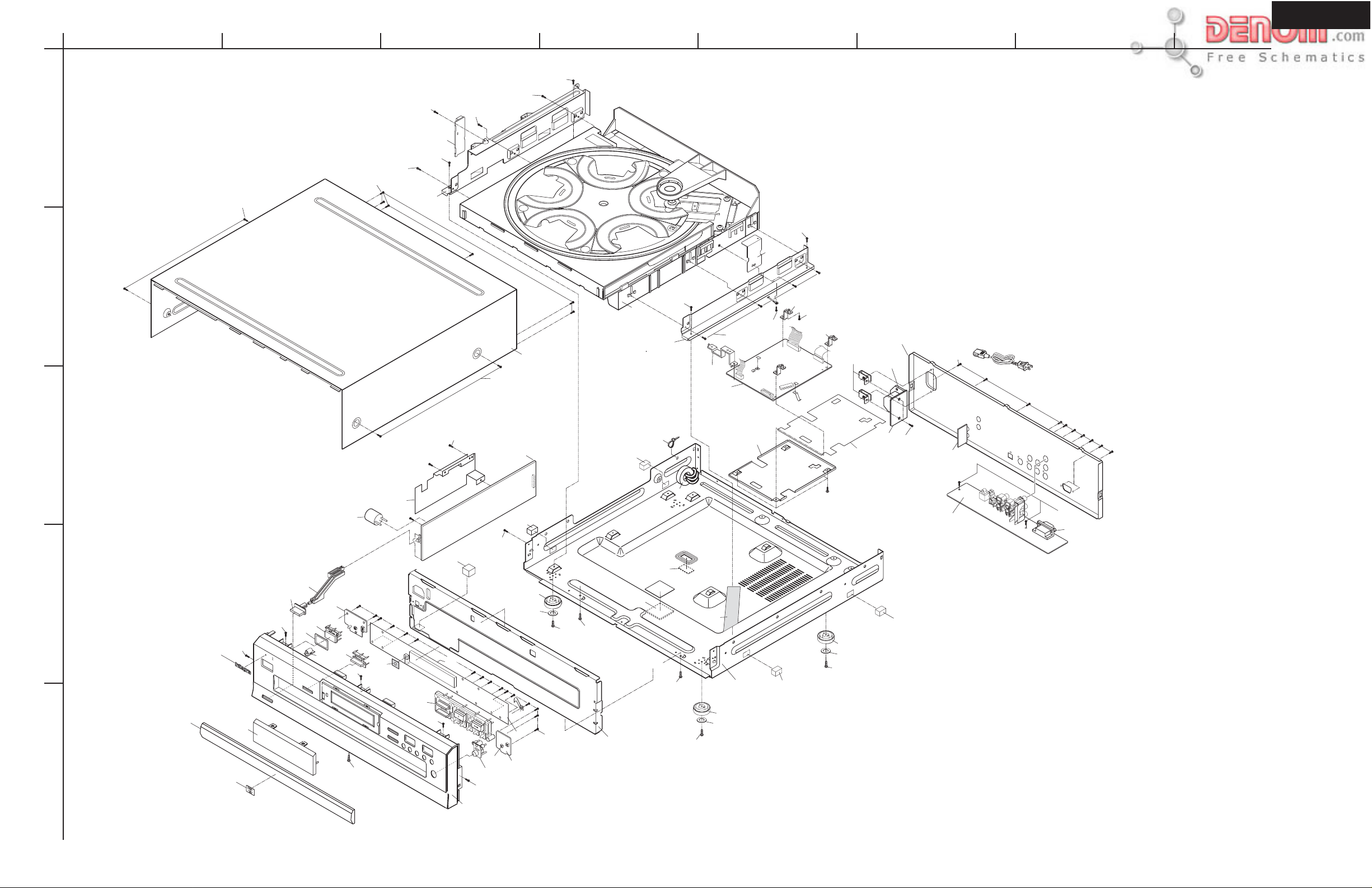
DP-C5.3
A
EXPLODED VIEW-1
CHASSIS
1
2
S3
BCDEFGH
S1
S3
1
S2
43
S1
2
42
S1
S2
50
49
41
40
S2
51
S2
51
56
39
S6
54
S6
S2
S2
S2
46
S1
44
48
55
23
S2
58
30
S2
36
16
S4
13
S2
22
S5
15
17
S2
18
19
52
23
20
24
25
S2
S2
S2
21
23
38
29
28
27
S2
24
25
S2
3
53
60
7
S4
8
10
9
6
11
5
S4
12
S2
4
S5
4
2
3
5
1
26
47
24
25
S2
23
14
www.denom.com
Page 5
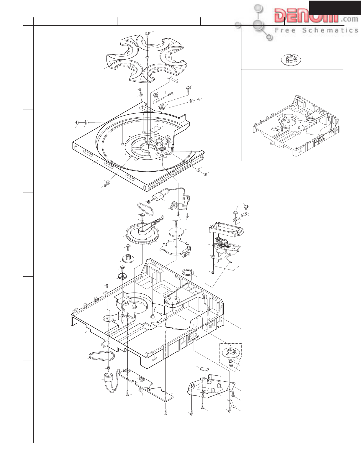
DPC-5.3
A
EXPLODED VIEW-2
DVD Mechanism
1
150
160
2
170
160
50
150
160
150
BCD
280
CLAMPER DVD ASS'Y
Part No. 55542660
130
90
120
110
100
140
240
150
160
150
160
BASE ASS'Y - CDM5G
Part No.55542650
70
80
280
420
3
270 * 2
200
240
220
240
230
60
310
300
* 2
320
210
470
480
290
450
* 4
460
* 4
280
* 2
440
430
4
190
260
250
70
530
Assy Part No.
55542660
490
510
550
520
300
560
300
5000
300
300
540
300
*2
300
500
5
www.denom.com
Page 6

DPC-5.3
A
BLOCK DIAGRAM -5
POWER SUPPLY UNIT
1
AC INPUT
2
SW1 F1
HOT >
NUT >
LINE FILTER
BCDE
FL OUTPUT
RECTIFIER &
SMOOTHING
CIRCUIT
R2
R3
SNUBBER
CIRCUIT
-27V OUTPUT
RECTIFIER &
SMOOTHING
CIRCUIT
-9V OUTPUT
RECTIFIER &
SMOOTHING
CIRCUIT
+12V OUTPUT
RECTIFIER &
SMOOTHING
CIRCUIT
+9V OUTPUT
RECTIFIER &
SMOOTHING
CIRCUIT
RECTIFIER &
SMOOTHING
CIRCUIT
+5V OUTPUT
RECTIFIER &
SMOOTHING
CIRCUIT
. DRIVER CIRCUIT
+5.5V OUTPUT
RECTIFIER &
SMOOTHING
CIRCUIT
. VOLTAGE CONTROLLER CIRCUIT
. OVER CURRENT PROTECTOR CIRCUIT
3
+3.5V OUTPUT
RECTIFIER &
SMOOTHING
CIRCUIT
+2.5V OUTPUT
RECTIFIER &
SMOOTHING
CIRCUIT
VOLTAGE
DETECTOR
CIRCUIT
PC1
4
www.denom.com
Page 7
DPC-5.3
A
BLOCK DIAGRAM -4
DVD MECHANISM & OUTPUT CIRCUIT
1
MECHANISM CONTROL PC BOARD
2
BCDE
AUDIO/VIDEO JACK
Main circuit PC board
3
PICK UP
Flat cable
AUDIO/VIDEO JACK
4
www.denom.com
Page 8
DPC-5.3
A
BLOCK DIAGRAM -3
DISPLAY SECTION
1
2
BCDE
From Power supply unit
To Main PC board
3
Key matrix
4
www.denom.com
Page 9
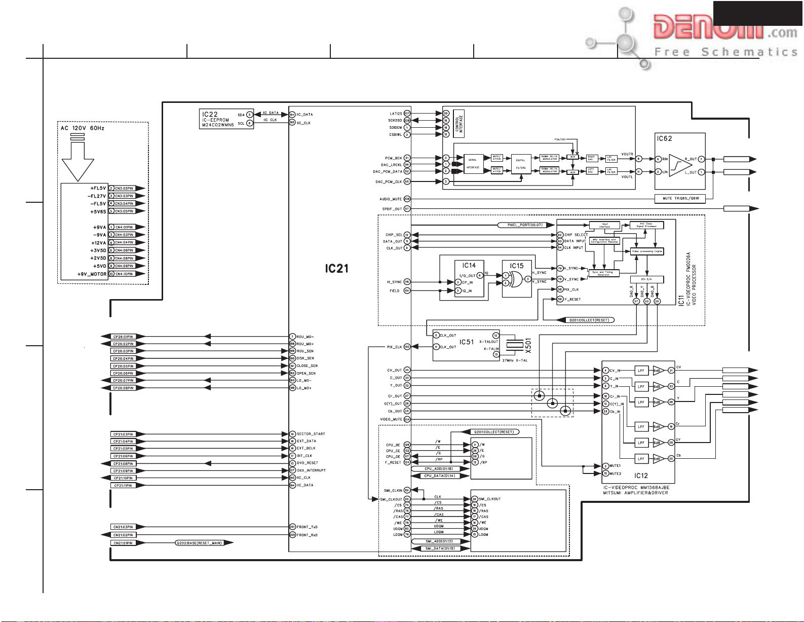
DPC-5.3
A
BLOCK DIAGRAM -2
1
POWER SUPPLY UNIT
2
To Mechanism control
BCDE
MAIN CIRCUIT BOARD
IC-LOGIC 74HC74
FLIF/FLOP CMOS
IC61
IC-CONV WN8728 D/A
IC-LOGIC 74HC86
GATE HCMOS
IC-OPEAMP
BA4560F
To OUT
CP25:04PIN
CP25:06PIN
To OUT
CN27:SPDIF
INVERTER HCT
IC-LOGIC M74HCU04M1R
IC- VIDEOPROC STI5519
MPEG VIDEO DECODER
3
To Pick up
IC41
IC MEMFLASH
M29W800A T901N1
TR SWITCH CIRCUIT
P SCAN ON/OFF
To OUT
CP25:08PIN
CP25:10PIN
CP25:12PIN
CP25:14PIN
CP25:16PIN
CP25:18PIN
IC31
To Display
IC-DRAM HY57V651620BTC-8
125M 64M(1M x 16 x 4)
4
www.denom.com
Page 10

DPC-5.3
A
BLOCK DIAGRAM-1
OVER ALL
1
2
BCDEFGH
3
4
5
www.denom.com
Page 11

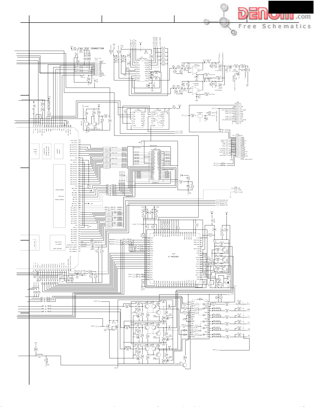
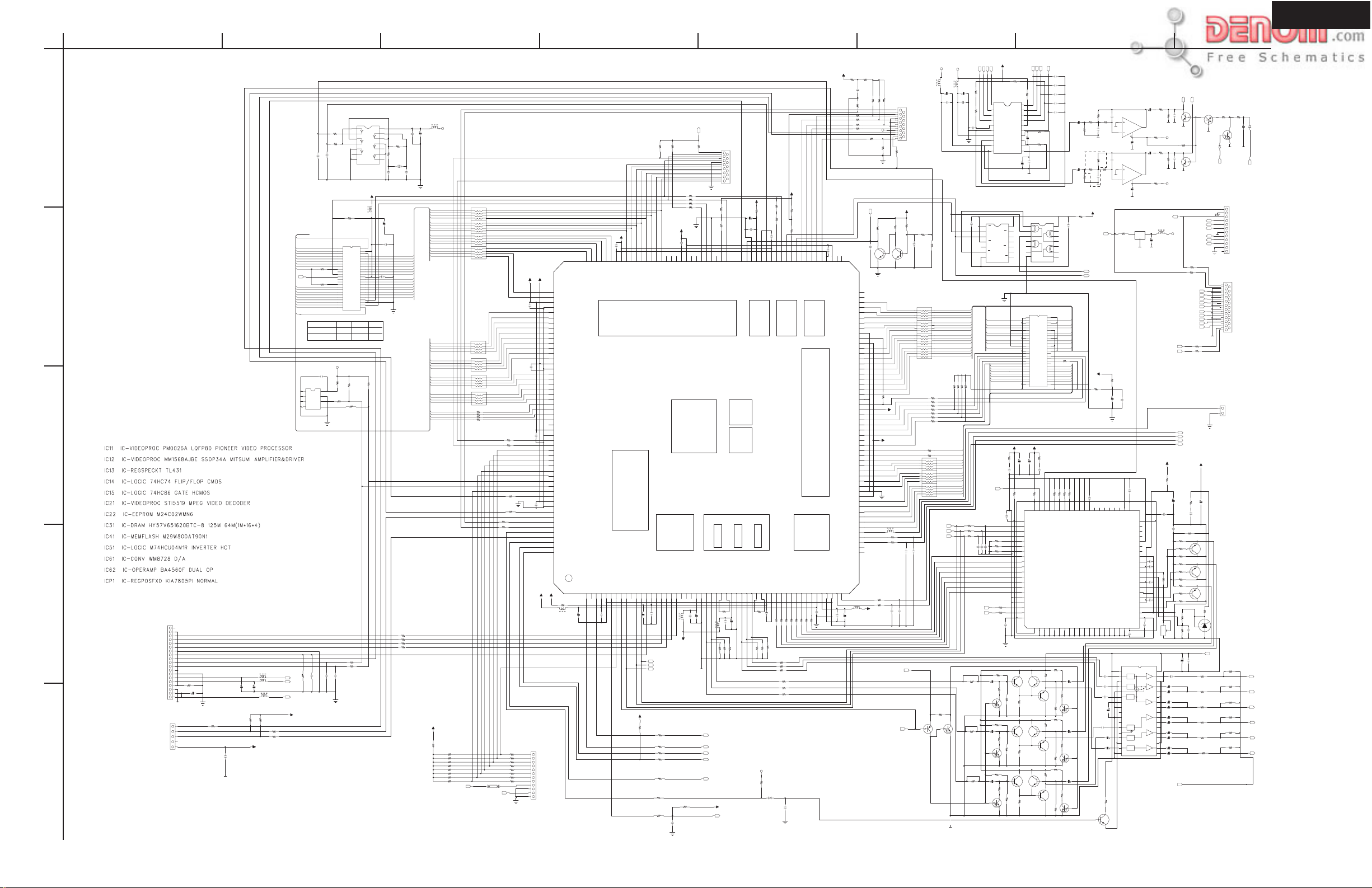
DV-CP500
A
SCHEMATIC DIAGRAM
Main circuit PC board-1
1
2
F_ADDR17
F_ADDR16
F_ADDR15
F-ADDR14
F_ADDR13
F_ADDR12
F_ADDR11
F_ADDR10
F_ADDR09
F_ADDR20
F_RESET
F_ADDR19
F_ADDR18
F_ADDR08
F_ADDR07
F_ADDR06
F_ADDR05
F_ADDR04
F_ADDR03
F_ADDR02
F_ADDR01
BCD
L501
FCM2012H-102T04
100R-03
R504
100R-03
R501
C501
C506
20P-03
20P-03
+3.3VM
47K-03
R413
IC41
IC-M29F400T-90N1
1
A15
A16
2
A14
BYTE
3
A13
VSS
4
A12
DQ15
5
A11
DQ7
6
A10
DQ14
7
A9
DQ6
8
A8
DQ13
9
NC
DQ5
10
NC
DQ12
R411
11
WE
DR-03
R412
DR-03
DQ4
12
RP
VCC
13
NC
DQ11
14
NC
DQ3
15
RY/BY
DQ10
16
A18
DQ2
17
A17
DQ9
18
A7
DQ1
19
A6
DQ8
20
A5
DQ0
21
A4
QE
22
A3
VSS
23
A2
CE
24
A1
A0
R415
ADD
48
47
46
45
44
43
42
41
40
39
38
37
36
35
34
33
32
31
30
29
28
27
26
25
FCM2012H-102T04
1M-03
R503
R502
56R-03
X501
X-TAL
C502
22P-03
C406
100/10
D3V3
C504
C505
100N-03
470/6.3
C503
22P-03
GND
Down load Jig
+5V6S
100N-03
C228
R245
IC22
10R-03
IC-M24C02
1
8
E0
VDD
2
7
E1
WC
R248
3
6
E2
SCL
47R-03
4
5
VSS
SDA
GND
R247
R246
1K8-03
1K8-03
R249
47R-03
3
4
CP21
FPC-19P Pickup to Main PCB
1
NC
2
D_GND
3
SECTOR_START
4
DATA_VALID
5
DATA
6
BIT_CLOCK
7
D_GND
8
RESET
9
DXX_INTERRUPT
10
SCL
11
SDA
12
D_GND
13
DRIVE_GND
14
+3V3D
15
+5VD
16
D_GND
17
A_GND
18
DISC_M_POWER
19
TRACK_M_POWER
From Display circuit PC board
(To Connection PCB)
5
To Mechanism control PCB (P406)
www.denom.com
Page 12
DPC-5.3
A
SCHEMATIC DIAGRAM
Main circuit PC board-2
1
2
BCD
To Power supply unit (CN2)
NC
NC
To Output terminal PCB (CN01)
NC
NC
To Output PCB (CP01)
3
4
Video signal out
5
www.denom.com
Page 13
DPC-5.3
A
SCHEMATIC DIAGRAM-1
MAIN CIRCUIT PC BOARD
1
2
3
4
CP21
FPC-19P From Pickup to Main PCB
1
NC
2
D_GND
3
SECTOR_START
4
DATA_VALID
(EXT_DATA)
5
DATA
(EXT_BCLK)
6
BIT_CLOCK
7
D_GND
(3V3_R)
8
RESET
(IRQ2)
9
DXX_INTERRUPT
10
SCL
11
SDA
12
D_GND
13
DRIVE_GND
14
+3V3D
15
+5VD
16
0R-03
D_GND
R250
17
A_GND
DISC_M_POWER
TRACK_M_POWER
5
18
19
AGND
CN21
CN-2.0-05P
1 RESET_MAIN
2 FRONT_TXD
3 FRONT_RXD
4 OPTION_NC
5 +5V6S
From Display circuit PC board
(to connection PCB)
47/16
C222
0R-03
R254
C233 100P-03
BCDEFGH
+3V3
MCLK_IN
BCK_IN
DATA_IN
47/16
C601
C602
C605
10P-03
GND
C133
SDATA07
SDATA06
SDATA05
SDATA04
4K7-03
4K7-03
R312
R313
SADDR(00:13)
R127 100R-03
R128 100R-03
R129 100R-03
10K-03
R22R
10K-03
DTC114YKA
100N-03
R22G
Q10G
10K-03
R22B
CTC114YKA
R615
4K7-03
R614
47R-03
C128 47P-03
VSYNC
HSYNC
Q10B
1
1RD
2
1D
3
1CP
4
1SD
5
1Q
6
1Q
7
GND
SDATA00
SDATA01
SDATA02
SDATA03
SDATA04
SDATA05
SDATA06
SDATA07
F_RESET
C127 47P-03
C126 47P-03
13K7-03-1%
DTC114YKA
LRC_IN
1
LRCIN
2
DIN
3
BCKIN
4
MCLK
5
ZERO
6
DGND
7
DVDD
8
VOUTR
9
AGND
10
AVDD
IC14
74AHC74
GND
SDATA(00:15)
SADDR12
SADDR13
SADDR10
SADDR00
SADDR01
SADDR02
SADDR03
R130 47K-03
R131 47K-03
R132 100R-03
R138 100R-03
R134 100R-03
R23R
10/16
C10R
5K6-03
Q10R
13K7-03-1%
R23G
10/16
C10G
5K6-03
13K7-03-1%
R23B
C10B
10/16
5K6-03
IC61
WM8728(SSOP)
14
VCC
13
2RD
12
2D
11
2CP
10
2SD
2Q
2Q
+2V5D
10R-03
1N-03
1N-03
C129
1N-03
GND
KTN2222
R12R
36K-03
KTN2222
R12G
36K-03
KTN2222
R12B
36K-03
SDIDEM
CSBIWL
9
8
C125
R13R
Q11G
R13G
R13B
R612
4K7-03
LAT125
SCKSD
MUTEB
MODE
VREFP
VREFN
VOUTL
R126
C123
Q11R
Q11B
VMID
+5VD
1: TRIGOUT
2: TRIGIN
3: GND(Option)
4: TMS
5: GND
6: TCK
7: GND
8: TDI
9: GND
10: TDO
11: +5VD
12: TDX(JIG)
13: RXD(JIG)
14: JTAG_RST/
15: TRST
R217
10K-03
10P-03
100N-03
10P-03
1
3
5
7
1
3
5
7
1
3
5
7
1
3
5
7
C206
C621
DTA114TS
1K-03
R218
R309
R308
R307
R306
R305
R304
R303
R302 100R-03
R301 100R-03
1
3
5
7
1
3
5
7
1
3
5
7
Q101
+5VA
L602
FCM2012H_102T04
R214
1K-03
RA37 47R
2
4
6
8
RA36 47R
2
4
6
8
RA35 47R
2
4
6
8
2
RA34 47R
4
6
8
100R-03
100R-03
100R-03
100R-03
100R-03
100R-03
100R-03
2
4
6
8
2
4
6
8
2
4
6
8
PM0026STB
PM0026DATA
PM0026CLK
R111
3K3-03
DTC114YS
RA33
AGND
560P-03
47R
RA32
47R
RA31
47R
10/50
C603
C604
Q102
L601
FCM2012H_102T04
560P-03
SDATA15
SDATA14
SDATA13
SDATA12
SDATA 11
SDATA 10
SDATA 09
SDATA 08
SDATA 03
SDATA 02
SDATA01
SDATA00
4K7-03
4K7-03
R310
R311
SASSR13
SADDR12
SADDR11
SADDR10
SADDR00
SADDR01
SADDR02
SADDR03
SADDR09
SADDR08
SADDR07
SADDR06
SADDR05
SADDR04
+3V3
R219
JTAG TEST CONNECTION
0R-03
R220
0R-03
C207
100N-03
47K-03
F_DATA15
F_DATA07
F_DATA14
F_DATA06
F_DATA13
F_DATA05
F_DATA12
F_DATA04
F_DATA11
F_DATA03
F_DATA10
F_DATA02
F_DATA09
F_DATA01
F_DATA08
F_DATA00
100R-03
100R-03
100R-03
100R-03
L501
FCM2012H-102T04
D3V3
C504
C505
100N-03
470/6.3
10K-03
C503
22P-03
GND
F_DATA(00:15)
F_ADDR(01:21)
F_ADDR01
F_ADDR02
F_ADDR03
F_ADDR04
F_ADDR05
F_ADDR06
F_ADDR07
F_ADDR08
F_ADDR09
F_ADDR10
F_ADDR11
F_ADDR12
F_ADDR13
F_ADDR14
F_ADDR15
F_ADDR16
F_ADDR17
F_ADDR18
F_ADDR19
F_ADDR20
+3V3D
0R-03
F_DATA00
F_DATA01
F_DATA02
F_DATA03
F_DATA04
F_DATA05
F_DATA06
F_DATA07
F_DATA08
F_DATA09
F_DATA10
F_DATA11
F_DATA12
F_DATA13
F_DATA14
F_DATA15
R260
R261
R262
R263
R264
R265
R266
R267
R268
+12V_MOTOR
RA41 47R
2
1
4
3
6
5
8
7
2
1
RA42 47R
4
3
6
5
8
7
RA43 47R
2
1
4
3
6
5
8
7
RA44 47R
2
1
4
3
6
5
8
7
+3V3 +2V5
157 CPU_DATA(14)
158 CPU_DATA(15)
159 VDD3_3
160 VSS
C214
100N-03
161 CPU_ADR(1)
162 CPU_ADR(2)
163 CPU_ADR(3)
164 CPU_ADR(4)
165 CPU_ADR(5)
47R-03
47R-03
47R-03
47R-03
47R-03
47R-03
47R-03
47R-03
GND
C215
100N-03
C216
C217
CN26
CP-2.0-AN-12P
1
2
3
4
5
6
7
8
9
10
11
12
100N-03
100N-03
166 CPU_ADR(6)
167 CPU_ADR(7)
168 CPU_ADR(8)
169 CPU_ADR(9)
170 CPU_ADR(10)
171 VDD2_5
172 VSS
173 CPU_ADR(11)
174 CPU_ADR(12)
175 CPU_ADR(13)
176 CPU_ADR((14)
177 CPU_ADR(15)
178 CPU_ADR(16)
179 CPU_ADR(17)
180 CPU_ADR(18)
181 CPU_ADR(19)
182 CPU_ADR(20)
183 CPU_ADR(21)
184 VDD3_3
185 VSS
186 PIO0(0) T_STROBE
187 PIO0(1) MOD_SW
188 PIO0(2)
189 PIO0(3)
190 PIO0(4)
191 PIO0(5)
192 PIO0(6) SLIDER_SENSOR_OPEN/VLOSE
193 PIO0(7) SLIDER_IN (DRAWER_CCW_CTRL)
194 PIO1(0) SDA
195 PIO1(1) SCL
196 PIO1(2) SLIDER_OUT (DRAWER_CW_CTRL)
197 PIO1(3) TXD(JIG)
198 VDD2_5
199 VSS
200 PIO1(4) RXD(JIG)
201 PIO1(5) FRONT_TXD1
202 TRIGGER_IN
203 TRIGGER_OUT
204 PIO2(0) VIDEO_MUTE
205 PIO2(1) FRONT_RXD
206 PIO2(2) AUDIO_MUTE
207 PIO2(3) DAC_LATI2S_OUT
208 PIO2(4) DAC_SCKDSD_OUT
+3V3 +2V5
L201
0R-03
2U2H
L202
C201
ROU-MOROU-MO+
ROU-SEN
DISC-SEN
CLOSE-SEN
OPEN-SEN
ID-MOID-MO+
+12V MOTOR
M GND
+5VD
M GND
100/10
RA45 47R
1
2
3
4
5
6
7
8
RA46 47R
1
2
3
4
5
6
7
8
RA47 47R
1
2
3
4
5
6
7
8
RA48 47R
1
2
3
4
5
6
7
8
47R-03
R407
47R-03
R408
47R-03
R409
47R-03
R410
47R-03
R239
47R-03
R240
47R-03
R241
47R-03
R242
R243
75R-03 TRIGIN
75R-03 TRIGOUT
R244
2R2-1/2W
R277
R269
R270
R271
R272
R273
R274
R275
R276
+5VD
47K-03
47K-03
47K-03
47K-03
47K-03
47K-03
47K-03
47K-03
+2V5
C213
100N-03
156
155
154
153
152
151
150
149
148
147
146
145
144
143
142
VSS
VDD2_5
CPU_DATA(9)
CPU_DATA(8)
CPU_DATA(13)
CPU_DATA(12)
CPU_DATA(7)
CPU_DATA(11)
CPU_DATA(10)
141
CPU_DATA(6)
CPU_DATA(5)
CPU_DATA(4)
CPU_DATA(3)
CUP_DATA(2)
CPU_DATA(1)
CPU_DATA(0)
FLASH MEMORY
3-PWM Outputs
12C Controller
2-UARTS
38-Bit Programable I/O
PIO2(5) DAC_SDIOEM_IN/OUT
PIO2(6) DAC_MUTEB_IN/OUT
PIO2(7) DAC_CSBIWL_OUT
VDD3_3
VSS
PIO3(0) PRO_SCAN_ON/OFF
PIO3(1)
PIO(2)
100N-03
PIO(3)
C202
12345678910111213141516171819
PIO3(4) IR(REMOTECONT)
B_DATA
PIO3(5)
PIO3(6)
PIO3(7) DVD_RESET
DVV2_5
VSS
C204
100N-03
C203
470/6.3
PM0026STB
PM0026DATA
PM0026CLK
+3V3D
R609
4K7-03
R613 47R-03
R611 47R-03
R610 47R-03
R608 47R-03
R607 47R-03
100R-03
R135
47R-03
R205
+5VD
DOWN LOAD JIG
10K-03
139
CPU_CAS0
R405
+3V3
100N-03
138
CPU_RAS1
R414
10R-03
15
14
13
12
11
10
9
8
7
6
5
4
3
2
1
GND
FPC-ST_15P
47R-03
47R-03
47R-03
47R-03
GND
135
134
CPU_CE(0)
CPU_CE(1)
CPU MEMORY
PROGRAMABLE
133
132
CPU_CE(2)
CPU_CE(3)
INTERFACE
CP22
R237
10K-03
R238
47R-03
131
130
129
128
CPU_RW
CPU_WAIT
CPU_BE(1)
CPU_BE(0)
R404
R403
R402
R401
C212
137
136
VSS
VDD3_3
R406
140
CPU_CAS1
IC21
STI5519
ST20 CPU
PAL/NTSC/SECAM ENCODER
10-BIT DAC
B_WCLK
B_V4
NRSS_OUT
VDD_RGB
VSS_RGB
B_out
G_OUT
R_OUT
V_REF_RG
C102
C101
100/10
AGND
I_REF_RG
18K-03
R101
10N-03
L102
2U2H
R10B
300R-03
DAC_CSBIWL_OUT
DAC_SDIDEM_IN/OUT
DAC_SCKSD_OUT
DAC_LATI3S_OUT
AUDIO_MUTE
+3V3D
PRO_SCAN_ON_OFF
21222324252627282930313233343536373839
20
10N-03
L101
2U2H
+2.5VA
R206
10K-03
B_BCLK
INTERFACE
FRONT-END
B_FLAG
B_SYNC
C229
10N-03
127
IRQ(0)
4KB SRAM
DATA-CACHE
INSTRUCTION
VDD_YCC
VSS_YCC
C104
R10R
R10G
300R-03
300R-03
126
IRQ(1)
CACHE
C103
122
PLL
R102
300R-03
+5VD
R236
121
VSS
10-BIT DAC
I_REF_YC
300R-03
R10Y
4K7(S)
1SS355(SMD)
100N-03
R136
120
PIX_CLK
VDD2_5
300R-03
R10C
D101
C209
119
VDD2_5
VSS
C105
R10S
+3V3
R234
10K-03
R232 10K-03
R235
47R-03
R233
10K-03
100N-03
118
117
116
115
114
113
TCK
PWM0
PWM1
PWM2
CPU_OE
CPU_PROCLK
DIAGNOSTICS
SYSTEM SERVICE
CONTROLLER AND
AUDIO DECODER
PIO4(0)
PIO4(1)
PIO4(2)
PIO4(3)
PIO4(4)
PIO4(5)
40
4142434445464748495051
47R-03
47R-03
47R-03
47R-03
47R-03
47R-03
R103
R104
R105
R106
R107
R108
10R-03
R11S
10R-03
R11C
10R-03
R11Y
R11R
10R-03
R11G
10R-03
R11B
10R-03
C132
100N(SMD)
GND
112
111
TDI
TDO
KARAOKE
MODULE
SDRAM MEMORY
INTERFACE
SHARED MEMORY
PCM OUT
6-CHANNEL
PIO4(6)
PIO4(7)
47R-03
47R-03
100N-03
R109
R110
+2V5
10R-03
C210
100/10
10N-03
C211
125
124
123
IRQ(2)
RESET
VSS_PLL
VDD_PLL
GENERATOR
CLOCK
2KB
2KB
10-BIT DAC
V_REF_YC
Y_OUT
C_OUT
CV_OUT
18K-03
100/10
IC51
74HCU04
1
14
FCM2012H-102T04
47K-03
R413
IC41
M29F400T-90N1
1
A15
2
A14
3
A13
4
A12
5
A11
6
A10
7
A9
8
A8
9
NC
NC
WE
RP
NC
NC
RY/BY
A18
A17
A7
A6
A5
A4
A3
A2
A1
R245
1K8-03
R249
47R-03
R252
100R-03
BYTE
DQ15
DQ14
DQ13
DQ12
DQ11
DQ10
R246
2
3
4
5
6
7
A16
VSS
DQ7
DQ6
DQ5
DQ4
VCC
DQ3
DQ2
DQ9
DQ1
DQ8
DQ0
VSS
R253
100R-03
VCC
13
12
11
1M-03
10
R503
9
R502
56R-03
8
GND
R415
ADD
48
47
46
45
44
43
42
41
40
39
38
37
36
35
34
33
32
31
30
29
28
QE
27
26
CE
25
A0
X501
X-TAL
C502
22P-03
+3.3VM
C406
100/10
1N-03
C405
1N-03
C404
GND
R247
1K8-03
R201
R202
R203
R204
100R-03
R504
100R-03
R501
C501
C506
20P-03
20P-03
F_ADDR17
F_ADDR16
F_ADDR15
F-ADDR14
F_ADDR13
F_ADDR12
F_ADDR11
F_ADDR10
F_ADDR09
F_ADDR20
F_RESET
F_ADDR19
F_ADDR18
F_ADDR08
F_ADDR07
F_ADDR06
F_ADDR05
F_ADDR04
F_ADDR03
F_ADDR02
F_ADDR01
1
2
3
4
FCM2012H-102T04
L203
L204
FCM2012H-102T04
47/16
47/16
C224
C223
FCM2012H-102T04
R259
R258
10K-03
10K-03
+5V6S
10K-03
+3V3
+5VD
L205
+9VM
+5V6S
R256
47R-03
R257
47R-03
10
R411
11
DR-03
12
13
R412
14
DR-03
15
16
17
18
19
20
21
22
23
24
R411 R412 R413
ATMEL 16M 0 ohm NC 4K7
ST 16M NC 0 ohm
+5V6S
100N-03
C228
IC22
10R-03
IC-M24C02
8
E0
VDD
7
E1
WC
R248
6
E2
SCL
47R-03
5
VSS
SDA
GND
R251
C226
C227
C225
68P-03
68P-03
100N-03
GND
110
TMS
VDD3_3]
109
TRST
VDD_PCM
C615
GND
108
VSS
VSS_PCM
C208
100N-03
107
106
105
VDD3_3
ADC_DATA
ADC_PCMCLK
ADC_LRCLK
ADC_SCLK
SMI_DATA(15)
SMI_DATA(14)
SMI_DATA(13)
SMI_DATA(12)
SMI_DATA(11)
SMI_DATA(10)
SMI_CLKOUT
VDD2_5
SMI_DATA(9)
SMI_DATA(8)
SMI_DATA(7)
SMI_DATA(6)
SMI_DATA(5)
SMI_DATA(4)
SMI_DATA(3)
SMI_DATA(2)
SMI_DATA(1)
SMI_DATA(0)
SMI_CLKIN
VDD3_3
SMI_DQMU
SMI_DQML
SMI_WE
SMI_CAS
SMI_RAS
SMI_CS(1)
SMI_CS(0)
SMI_ADR(13)
SMI_ADR(12)
SMI_ADR(11)
SMI_ADR(10)
SMI_ADR(0)
SMI_ADR(1)
SMI_ADR(2)
SMI_ADR(3)
VDD2_5
SMI_ADR(9)
SMI_ADR(8)
SMI_ADR(7)
SMI_ADR(6)
SMI_ADR(5)
SMI_ADR(4)
SPDIF_OUT
(LRCIN) DAC_LRCLK
(MCLK) DAC_PCMCLK
DAC_PCMOUT2
DAC_PCMOUT1
VSS
DAC_SCLK (BCK)
DAC_PCMOUT0 (DATA)
52
PCM_DATA_OUT R617 47R-03
PCM_BCK_OUT R616 47R-03
C616
10N-03
C617
100/10
R225 47R-03
R226 47R-03
R227 47R-03
R228 47R-03
VSS
VSS
VSS
104
103
102
101
100
79
78
77
76
75
74
73
72
71
70
69
68
67
66
65
64
63
62
61
60
59
58
57 SPDIF
56 PCM_LR$CIN
55 PCM_MCLK
54
53
L603
2U2H
R221
R229 47R-03
99
98
97
96
95
94
93
92
91
90
89
88
87
86
85
84
83
82
81
80
470P-03
+2V5
F_RESET
C205
R222 10K-03
R223 10K-03
10K-03
R215
4K7-03
Q201
KTC3875(S)
GND
0R-03
GND
R224 10K-03
R230
GND
J301
+3V3
+2V5
L604
47R-03
R618
100R-03
C618
PROG_H
R619
10P-03
FPC_ST_15P
CP23
1
2
3
4
5
6
7
8
9
10
11
12
13
14
15
R231
R216
4K7-03
Q202
KTC3875(S)
BEAD 120 ohm
C620
C619
+3V3D
0R-03
+3V3
10P-03
DAC_CSBIWL
DAC_LAT125
DAC_SCKDSD
DAC_SDIOEM
10P-03
C613
10P-03
C612
10P-03
R605
C611
47K-03
10P-03
20
C610
19
10P-03
18
C609
NC
NC
A9
A8
A7
A6
A5
A4
R125
C121
CLK
VIB8
680(SMD)
680(SMD)
R15B
VCC
54
53
52
51
50
49
48
47
46
45
44
43
42
41
40
39
38
37
36
35
34
33
32
31
30
29
28
GND
VIB7
13K7-03-1%
R24R
13K7-03-1%
13K7-03-1%
680(SMD)
14
13
12
11
10
9
8
SDATA15
SDATA14
SDATA13
SDATA12
SDATA11
SDATA10
SDATA09
SDATA08
R315 47K(SMD)
SADR11
SADDR09
SADDR08
SADDR07
SADDR06
SADDR05
SADDR04
R122 47K-03
R121 47K-03
RAM2
RAM3
VIB6
VIB5
5K6-03
R16R
36K-03
R24G
5K6-03
R16G
36K-03
R24B
5K6-03
R16B
36K-03
C61L
47/16
R61L
47K-03
C61R
47/16
47K-03
R147
10R-03
C134
100N-03
R120 47K-03
R119 47K-03
GND
GND
GND
RAM4
RAM5
IC
PM0026A
VIB4
VIB3
GND
GND
GND
1011121314151617181920
C11R
10/16
R17R
Q14R
DTC114YKA
C11G
10/16
R17G
Q14G
DTC114YKA
10/16
C11B
R17B
Q14B
DTC114YKA
KTC3875(S)
17
16
33R-03
15
R602
14
13
C608
100/10
33R-03
12
R601
11
C607
C606
10/16
560P-03
AGND
IC15
74AHC86
1
2
3
4
5
6
7
GND
SDATA(00:15)
IC31
SDRAM_4Mx16
VSS
1
VCC
DQ15
2
DQ0
VSSQ
3
VCCQ
DQ14
4
DQ1
DQ13
5
DQ2
VCCQ
6
VSSQ
DQ12
7
DQ3
DQ11
8
DQ4
VSSQ
9
VCCQ
DQ10
10
DQ5
DQ9
11
DQ6
VCCQ
12
VSSQ
DQ8
13
DQ7
VSS
14
VCC
15
LDQM
UDQM
16
WE
CLK
17
CAS
CKE
18
RAS
19
CS
A11
20
BA0
21
BA1
22
A10
23
A0
24
A1
25
A2
26
A3
VSS
27
VCC
SADDR(00:13)
+3V3D
10R-03
C122
C124
100/16
100/16
1N-03
R124
R123
2R2-03
2R2-03
60595857565554535251504948474645444342
SRN
VDD3
61
VDD2
62
CSB
63
SDTA
64
SCLK
65
RAM1
66
RAM0
67
CKPOL
68
VIA9
69
VIA8
70
VIA7
71
VIA6
72
VIA5
73
VIA4
74
VIA3
75
VIA2
76
VIA1
77
VIA0
78
NVS
79
NHS
80
VDD3
VDD3
VIB9
123456789
Q12R
KTN2222
R15R
Q13R
R14R
2K2-03
KTN2907A
Q12G
KTN2222
R15G
Q13G
R14G
2K2-03
KTN2907A
Q12B
KTN2222
Q13B
R14B
KYN2907A
2K2-03
AUDIO_L
C67L
R66L
100P-03
100K-03
Q61L
DTC323TK(S)
-9V
820K-03
R606
C67R
R66R
100P-03
100K-03
Q61R
DTC323TK(S)
+9V
-9V
L210
+5VA
(VIDEO_AUDIO)
W4 0R_03
W3 0R_03
AUDIO_R
R_OUT(Cr)
G_OUT(Y)
B_OUT(Cb)
PRO_SCAN
TXD
RXD
PCM_LRCIN_OUT
PCM_DATA_OUT
PCM_BCK_OUT
PCM_MCLK_OUT
+2V5A +5VA
R118
2R2-03
C117
100/16
100N-03
C118
C114
1N-03
R18R 1K(SMD)
100(SMD)
R19R
R20R 75(SMD)
R18B 1K(SMD)
100(SMD)
R19B
R20B 75(SMD)
R115
R18G 1K(SMD)
360R-03
100(SMD)
R19C
R20G 75(SMD)
R113
3K6-05
1
3
200
VR11
0.5%
R112
1K4-05
2
G
C130
10N-03
100/16
100N-03
C13C
C13S 100/16
C14S 22/16
13Y 100/16
C14Y 22/16
C13G 100/16
C14G 22/16
C13B 100/16
C14B 22/16
C13R 100/16
C14R 22/16
AGND
AUDIO_R
+12V_SCART
+5V5S
+3V5D
+2V5D
+9V_MOTOR
AUDIO_L
CVBS
C_OUT
Y_OUT
+5VD
R207 47R_03
R208 47R_03
R117
10R-03
C116
1N-03
2R2-03
R116
0.5%
3
C113
100N-03
C131
75R-03
75R-03
470R-03
0R-03
R605
R604
330/6.3
Q602
DTA114YKA
AGND
C115
Q15R
Q15B
Q15G
82R-03
2
1
KTN2907A
KTN2907A
KTN2907A
R114
DTC114YKA
1SS355(SMD)
FPC_ST_23P(6216)
CP_2.0_ST_02P
1
2
TL431
+5VA
D601
A_MUTE
CN25
CN_2.5_12P
1
2
3
4
5
6
7
8
9
10
11
12
CP25
1
2
3
4
5
6
7
8
9
10
11
12
13
14
15
16
17
18
19
20
21
22
23
CN27
1.SPDIF
2.D_GND
10K-03
10K-03
10K-03
10K-03
R29C
10K-03
R29B
10K-03
R29R
C614
+9V
A_GND
-9V
+12V_SCART
+5V6S
+3V5D
D_GND
+2V5D
+5VD
+9V_MOTOR
M_GND
NC
1. DGND
2. SPDIF
3. AGND
4. AUDIO_R
5. AGND
6. AUDIO_L
7. AGND
8. CVBS
9. AGND
10. C_OUT
11. AGND
12. Y_OUT
13. AGND
14. R_OUT(Cr)
15. AGND
16. G_OUT(Y)
17. AGND
18. B_OUT(Cb)
19. +5VD
20. NC
21. PRO_SCAN_ON_OFF
R29C
R29S
R29Y
1N414B
CVBS
D602
+9VA
C
Y
CY
Cb
Cr
Q601
+5VD
100/16
IC13
R25C
75R-03
R25S
75R-03
R25Y
75R-03
R25G
R25B
75R-03
R25R
100R-03
47/16
R65L
C66L
R62L
4K7-03
C62L
R62R
4K7-03
C32R
R61R
IC62-A
R64L
BA4560
C63L
9K1-03
330P-03
3
R63L
3K9-03
2N7-03
R64R
9K1-03
R63R
3K9-03
2N7-03
1
OUT
2
330R-03
R67L
C65L
47/16
100R-03
AGND
47/16
R65R
C66R
BA4560
C63R
IC62-B
330P-03
5
7
OUT
6
330R-03
8
R67R
47/16
C65R
AGND
+3V3D
KIA7805API
FCM2012H-102T04
IC1P
0R-03
+9V
1N-03
Q103
V_SYNC
H_SYNC
VDD3
VIB2
R21P
+3V3
L301
0R-03
0R-03
R314
C311
100/10
100N-03
GND
C120
VO0
VO1
GND
SPR0/VO2
SPR1/VO3
SPR2/VO4
SPR3/VO5
VIB1
VIB0
DOS1
DOS0
TEST2
TEST1
TEST0
1
VCC1
10N-03
2
CIN
C12C
3
MUTE1
100N-03
4
VIN
C12S
5
SELECT
100N-03
6
YIN
C12Y
7
BIAS
8
GND1
C106
9
NC
22/16
10
GND1
11
NC
100N-03
12
CY
C12C
13
CLP
C12B
14
Cb
1/50
15
MUTE2
C12R
16
Cr
1/50
17
GND2
R137
1K(SMD)
C312
SPR4/VO6
SPR5/VO7
SPR6/VO8
SPR7/VO9
41
VDD3
CLMP
AGND
AVDD2
FSADJ
AVDD2
DAO_R
AGND
DAO_B
AVDD2
DAO_Y
AGND
VDD3
1N-03
IC-MM1568
LPF
LPF
LPF
LPF
LPF
LPF
C21P
100/10
C119
1N-03
VDD3
40
39
38
37
GND
36
35
34
33
100N-03
VG
32
C112
31
C111
1N-03
30
VREF
29
C110
28
1N-03
27
26
25
24
C109
1N-03
23
22
VDD2
21
C108
1N-03
C107
IC12
34
VCC2
33
C
6dB
32
GND2
31
CVBS
6dB
30
29
GND2
28
Y
6dB
27
26
GND2
25
CY
6dB
24
23
GND2
13.5MHz
22
Cb
6dB
21
13.5MHz
20
GND2
19
Cr
6dB
13.5MHz
18
www.denom.com
Page 14
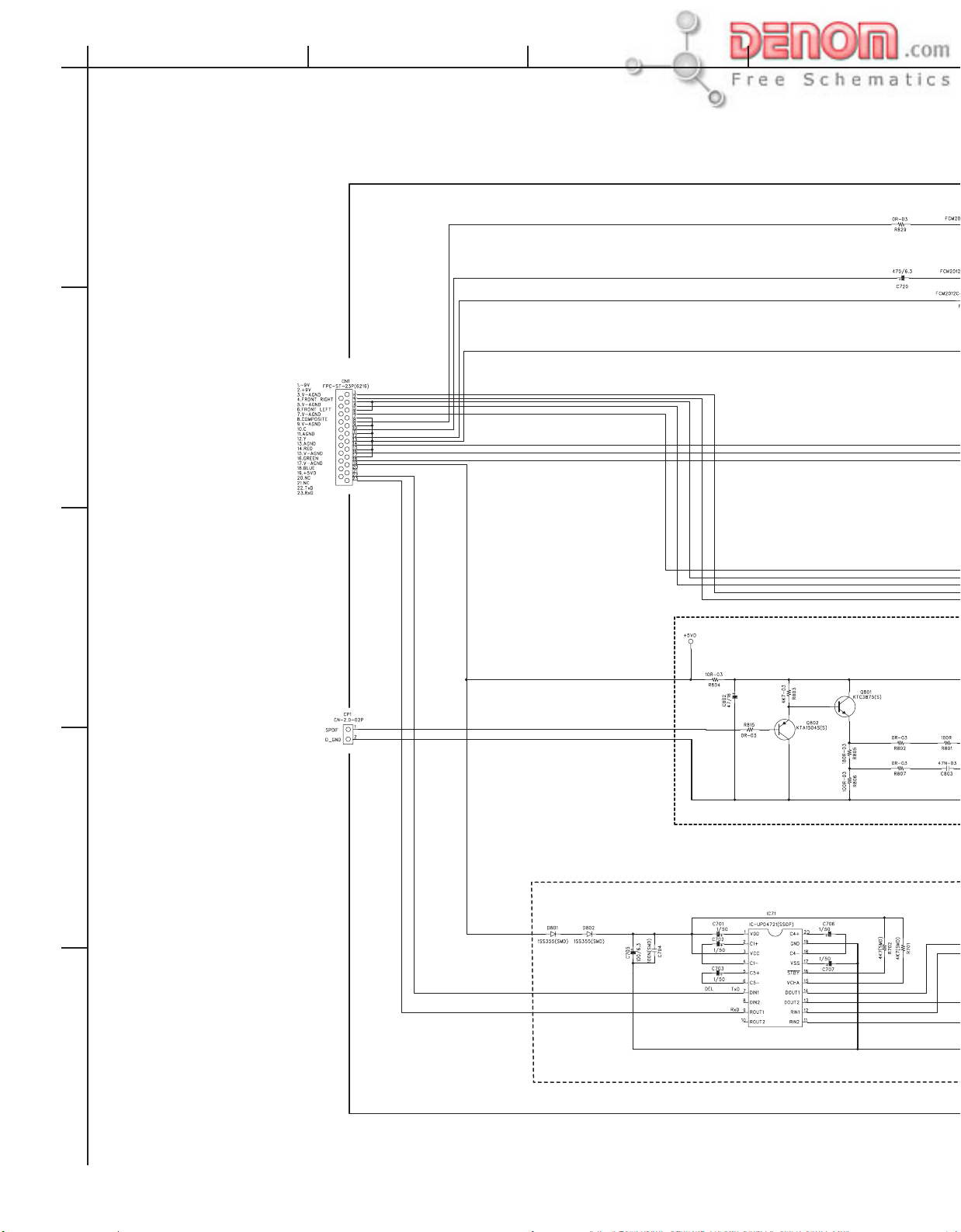
A
SCHEMATIC DIAGRAM-2
BCDEFGH
1
OUTPUT TERMINAL PC BOARD
From Main PCB
2
3
4
RS-232C TERMINAL
5
www.denom.com
Page 15

VIDEO OUT
S-VIDEO OUT
VIDEO
DPC-5.3
RI IN/OUT JACJ PC BOARD
COMPONENT OUT
1K
NC
NC
NC
NC
100R
100R
1K
FILTER CIRCUIT
www.denom.com
Page 16

DPC-5.3
A
SCHEMATIC DIAGRAM-2
1
2
BCDEFGH
OUTPUT TERMINAL PC BOARD
From Main PCB
VIDEO OUT
S-VIDEO OUT
RI IN/OUT JACJ PC BOARD
VIDEO
COMPONENT OUT
1K
NC
NC
NC
NC
3
100R
100R
1K
4
RS-232C TERMINAL
5
FILTER CIRCUIT
www.denom.com
Page 17

From Power supply unit
DPC-5.3
FL Tube
FL91
www.denom.com
Page 18

A
SCHEMATIC DIAGRAM
1
2
BCDEFGH
DISPLAY CIRCUIT PC BOARD
3
STANDBY LED PC BOARD
To OUTPUT TERMINAL PC BOARD
To Standby LED
To Front
4
5
www.denom.com
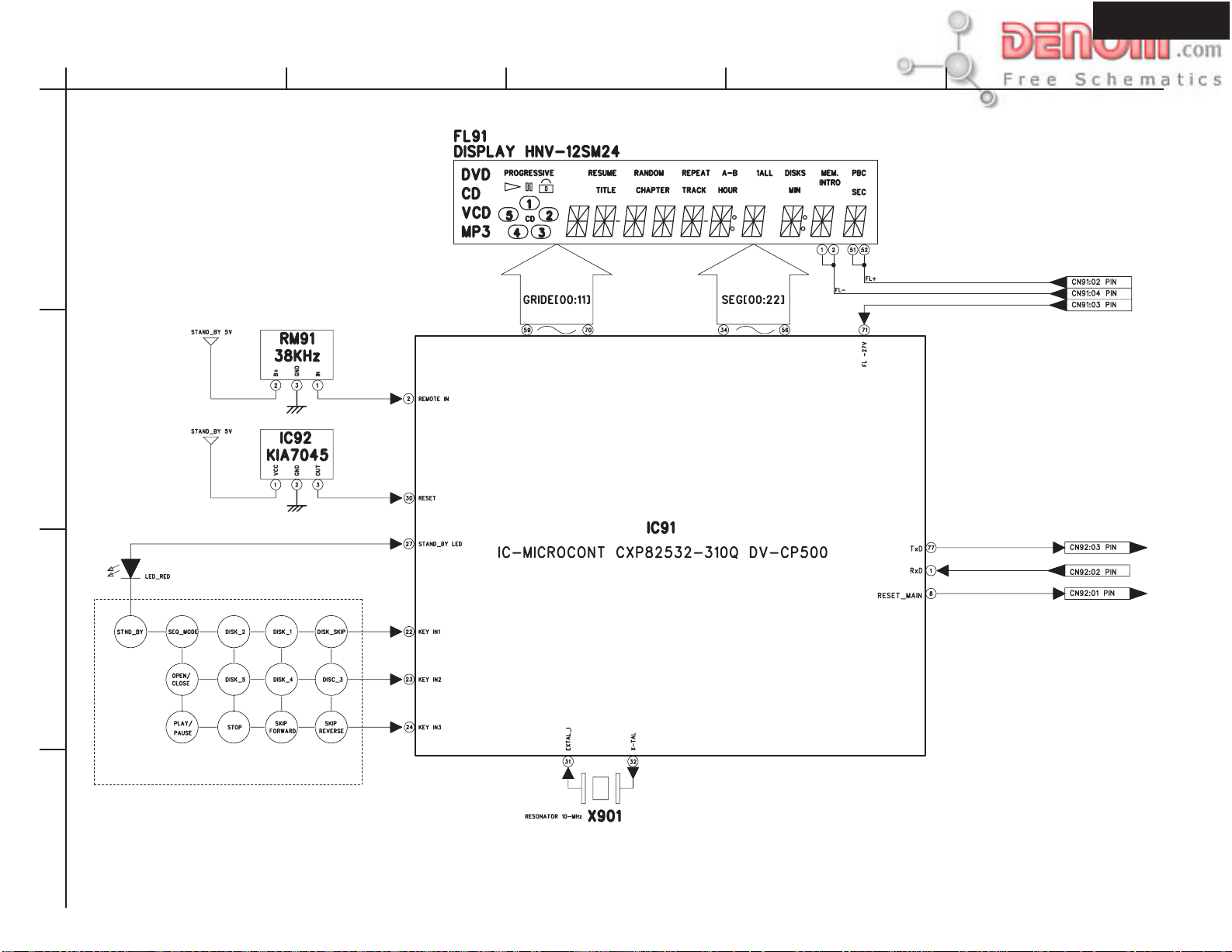
Page 19

DPC-5.3
A
SCHEMATIC DIAGRAM
1
2
BCDEFGH
DISPLAY CIRCUIT PC BOARD
From Power supply unit
FL Tube
FL91
3
STANDBY LED PC BOARD
To OUTPUT TERMINAL PC BOARD
To Standby LED
To Front
4
5
www.denom.com
Page 20

DPC-5.3
A
SCHEMATIC DIAGRAM 5
POWER SUPPLY UNIT
1
SW1
F1
TNR1
10471K
250V2A
1/4W
R1
1M
AC
POWER
2
NOTE
1. Resistor values are indicated in ohms
unless otherwise specified
( K = 1.000 M = 1.000.000 )
2. Capacitor values are indicated in
3
microfarades or picofarades
( :microfarades :pocofarades)
CAUTION
Safety precaution to be followed during
servicing
1) Since those parts marked with
are critical parts for safety.
use only the one described in the parts list.
2) Before returning the set to the customer
make apprppriate laekage current or
resistance measurements to determine the
exposed parts are prpperly insulated from
the supply circuit.
BCDE
D7
R40
1N5819
2.2
C4
630V472
R3
330K
D6
1N4148
C6
50V22
T1
EER2828
R4
22
C21
152Y1
C10
1KV102
R41
3.3
R39
2.2
D10
SR206
SR204
D12
SR204
C17
10V1000
D8
UF4003
D9
UF4003
L3
4.7uH
R9
C11
4.7
25V470
D11
C14
10V1000
R21
1K
L2
4.7uH
PC18
817
NT1
10D-9
ZD3
9.1V
C3
200V100
C19
1KV101
1
C5
333
R2
2W47K
D5
UF4007
U1
KA1L0365R
VCC
FB
LF1
C1
104
20MH
C2
104
D1-D4
1N4007
C22
101
C23
102
R5
C7
1K
10V470
R6
10
ZD1
3.3V
C8
R7
50V100
4.7K
C9
R8
50V100
1K
U3
KA7809
C18
10V470
D13
SR1A0
IO
G
R18
1K
D14
1N4007
R19
330
R20
330
C13
50V22
C12
R15
R10
18K
R13
2.2K
680
R16
150
R17
820
25V470
C16
10V470
L1
4.7uH
R14
R22
1.5KF
100
PC1/A
C15
50V1
U2
431
1
GND
2
+FL
3
-27
4
-FL
5
+5.65
CN1
1
+B
2
GND
3
-12V
4
+12V
5
RST
6
+2.5
7
GND
8
+2.5
9
+5
10
+9
11
GND
12
NC
CN2
4
www.denom.com
Page 21

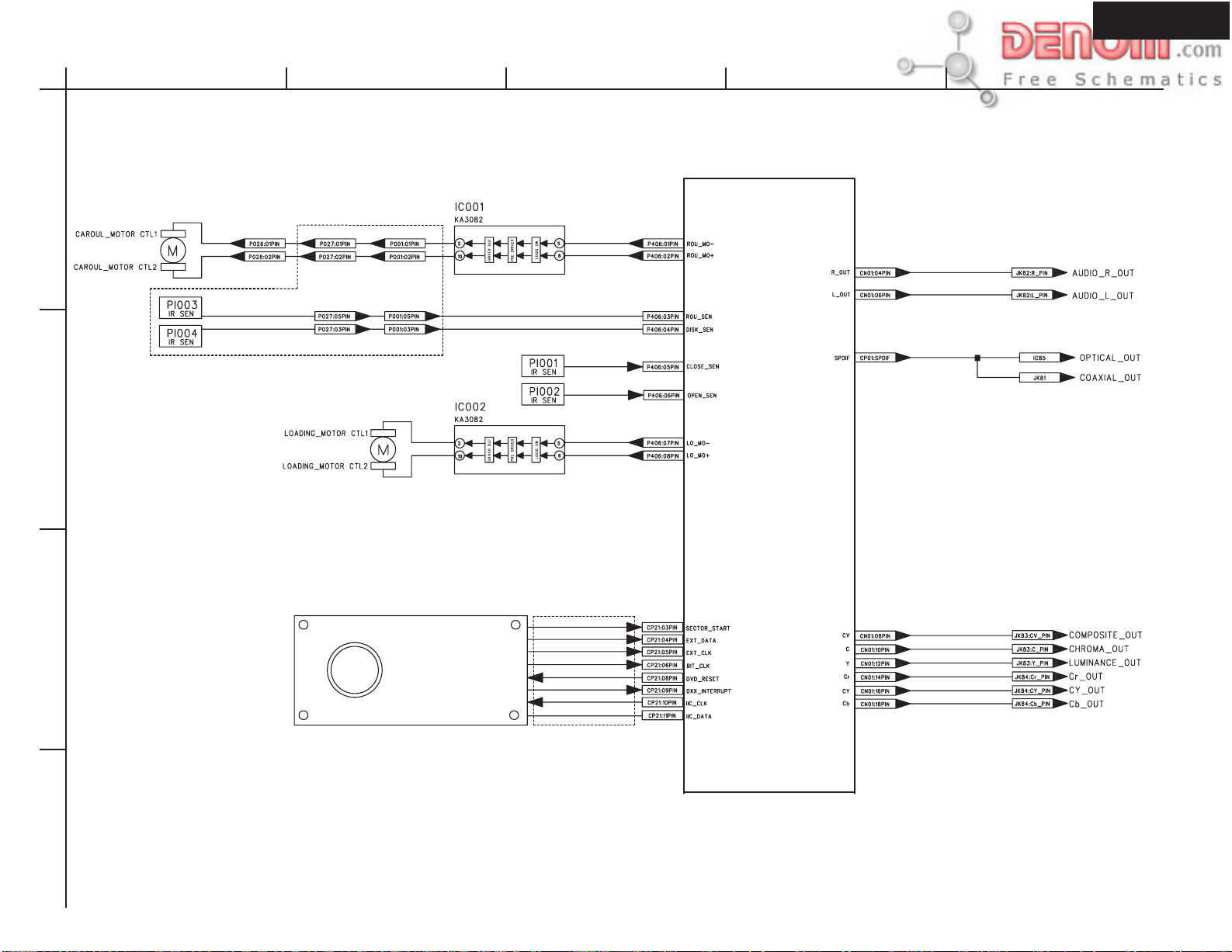
DPC-5.3
A
SCHEMATIC DIAGRAM 4
MECHANISM SECTION
1
2
BCDE
3
4
CAROUSEL MOTOR PC BOARD
www.denom.com
Page 22

PC BOARD CONNECTION DIAGRAM
DPC-5.3
AC120V 60Hz
STANDBY LED
CN2
CN1
POWER SUPPLY UNIT
CN3
CP94
CP95
CN96CN91
CP96
CN25
MAIN CIRCUIT
CN27
CN21
CN92
PC BOARD
CP22
FFC
CP25
CN01
CP21
MECHANISM CONTROL
CN26
FFC
To Roulette
motor
PC BOARD
Roulette motor
PC board
DISPLAY CIRCUIT PC BOARD
RI IN/OUT JACK
PC BOARD
CP01
OUTPUT TERMINAL PC BOARD
P406
P003
P027
RS-232C
TERMINAL
TRAVERSE MECHA.
B10
CN93
STANDBY LED PC BOARD
www.denom.com
OPEN/CLOSE
SWITCH PC BOARD
CP93
OPEN/CLOSE
Page 23

DPC-5.3
A
PRINTED CIRCUIT BOARD VIEW 1
MAIN CIRCUIT PC BOARD
1
2
BCD
3
4
5
Bottom pattern and Bottom component
www.denom.com
Page 24

DPC-5.3
A
PRINTED CIRCUIT BOARD VIEW 1
MAIN CIRCUIT PC BOARD
1
2
BCD
3
4
5
Top pattern and Top component
www.denom.com
Page 25

A
BCDEFGH
PRINTED CIRCUIT BOARD FROM SOLDERING SIDE VIEW 2
1
Display circuit PC board
2
CN93
S927
PLAY/PAUSE
S907
DISC5
S924
DISC4
S921
DISC3
S917
STOP
S905
DISC2
S915
DISC1
FF
S903
DISC SKIP
S911
FR
S901
J902
Component side
3
4
S905
S915
S917
S927
S907
S924
S921
5
www.denom.com
Page 26

DPC-5.3
J901
Component side
J920
FL91
C909
RM91
CN92
+
+
+
C907
+
C901
C906
J904
J903
S913
CN91
CN96
IC91
Soldering side
FL91
www.denom.com
CN92
S913
CN91
CN96
Page 27

DPC-5.3
A
BCDEFGH
PRINTED CIRCUIT BOARD FROM SOLDERING SIDE VIEW 2
1
Display circuit PC board
2
CN93
S927
PLAY/PAUSE
S907
DISC5
S924
DISC4
S921
DISC3
S917
STOP
S905
DISC2
S915
DISC1
FF
S903
DISC SKIP
S911
FR
S901
J902
J901
J920
FL91
C909
RM91
CN92
+
+
+
C907
+
C901
C906
J904
J903
S913
CN91
CN96
Component side
3
4
CN92
S913
CN91
CN96
S927
S907
S924
S921
S917
S905
S915
FL91
IC91
Soldering side
5
www.denom.com
Page 28

DPC-5.3
A
BCDEFGH
PRINTED CIRCUIT BOARD FROM SOLDERING SIDE VIEW 3
1
2
Output terminal PC board
9 8 7 6
5 4 3 2 1
JK83
JK82
CP01
JK81
IC85
C802
+
CN01
D711
Component side
3
9 8 7 6
5 4 3 2 1
4
Soldering side
5
www.denom.com
Page 29

A
BCDEFGH
PRINTED CIRCUIT BOARD FROM SOLDERING SIDE VIEW 3
1
Output terminal PC board
9 8 7 6
5 4 3 2 1
2
Component side
3
9 8 7 6
5 4 3 2 1
4
Soldering side
5
www.denom.com
Page 30

DPC-5.3
JK83
JK82
CP01
JK81
IC85
C802
+
CN01
D711
Soldering side
www.denom.com
Page 31

A
BCDEFGH
PRINTED CIRCUIT BOARD VIEW FROM SOLDERING SIDE 4
Roulette motor PC board
1
D-PHOTO RP1574/GP1S58V
P1003
D-PHOTO GP2S28
WCL 060-05 UL24
P1004
Component side view
2
Mechanism control PC board
3
JW13
JW17
JW6
JW21
JW3
JW7
R001
4
5
www.denom.com
Page 32

Ri IN/OUT Jack PC board
Component side view
DPC-5.3
R002
C002
JW14
C003
R003
JW22
C004
Component side view
R004
JW18
JW8
JW10
C001
D001
D002
IC001
JW20
IC002
L001
C005
JW15
-
Soldering side view
www.denom.com
Page 33

DPC-5.3
A
BCDEFGH
PRINTED CIRCUIT BOARD VIEW FROM SOLDERING SIDE 4
Roulette motor PC board
1
D-PHOTO RP1574/GP1S58V
P1003
D-PHOTO GP2S28
WCL 060-05 UL24
Component side view
2
P1004
Ri IN/OUT Jack PC board
Component side view
Mechanism control PC board
R004
JW18
JW8
JW10
C001
D001
D002
IC001
JW20
IC002
L001
C005
JW15
-
C002
3
JW13
JW17
JW6
JW21
JW3
JW7
R001
R002
JW14
C003
R003
JW22
C004
Component side view
4
5
Soldering side view
www.denom.com
Page 34

DPC-5.3
A
BCD
PRINTED CIRCUIT BOARD FROM SOLDERING SIDE VIEW 5
1
Connection PC board
CP94
2
Standby LED PC board
CP96
Component side
S931
D905
CP95
Soldering side
3
Soldering side
Inlet terminal PC board
OPEN/CLOSE Switch PC board
4
CP93
OPEN/CLOSE
S930
Soldering side
Soldering side
5
www.denom.com
Page 35

FW DOWNLOAD
Confirm the firmware
"CD PLAY" button and "DISC 3" button on the front panel
should be pressed at the same time. --------- Factory EEPROM reset.
Wattching the version of firmware in the FL tube.
When the name of the binaly file you wantto downloding is "dvcp5111.bin",
you may type "ttcmake dpc5.3fw1" in thr DOS prompt.
Space
Adifferent bin file requires a new data.
1. "TTCMAKE.EXE" file is downloaded to its own personal computer. (C-Drive)
DPC-5.3
2. "dvcp5111.bin" file is downloaded to its own personal computer.
(The same drive as 1.)
3. Call the "ttcmake dvcp5111" in the DOS prompt.
4. Call the file name of "dpc5.3" holder, and
"ttcmake dvcp5111" .
5. Created the "ENTRISE. TTC" Fig. 3
6. File created by 5. is copied to CD-R.
Caution: File format should be "ISO9660"
Fig. 2
TTCMAKE.EXE : application file
dvcp5111.bin : Binaly file
dps5.3
C: >cd..
C: cd dpc5.3
cd dpc5.3
dps5.3
Fig. 1
Fig. 1
C: dpc5.3>ttcmake dvcp5111
www.denom.com
dpc5.3
Fig. 2
Fig. 3
Page 36

DISASSEMBLY PROCEDURE
Replacement of DVD mechanism
The laser diode in the optical pickup block so
sensitive to static electricity, surge current and
etc..
That the components are liable to be broken down
or its reliability remarkable deteriorated.
During repair, carefully take the
following precautions.
Do not touch the optical
pickup object lens with the
hands.
1. Remove the top cover with six screws.
2. Remove the tray.
3. Remove the roulette assembly.
4. Remove the roulette. (Roulette is removed as written below.)
5. Solder the LD output lands on the DVD optical pickup.
Please perform right photo to reference.
6. Replace the pickup mechanism assembly etc. . After unsolder the laser diodes
output lands.
DPC-5.3
Short Land
Remove the roulette
1. Pull out the tray.
2. Stops in the position (cut deeply).
3. Remove in the direction of arrow.
4. Reassembly is performed by 3 to 1.
Roulette
Cut deep
www.denom.com
Page 37

P A CKING VIEW
DPC-5.3
240
RC-503DV
250
220
100
80
150
120
60
110
50
130
210
170
105
205
230
DPC-5.3
Rear side
www.denom.com
Page 38

PRINTED CIRCUIT BOARD PARTS LIS
T
R
D
R
R
R
R
G
R
D
R
L
R
R
F
W
%
%
W
%
%
M
A
A
A
M
M
M
A
A
A
W
W
MAIN CIRCUIT PC BOARD
CIRCUIT NO. PART NO. Pkg Unit DESCRIPTION
C13B 20269020 30 PCE CE 100U0F +20% 16.0V 85C
C13G 20269020 30 PCE CE 100U0F +20% 16.0V 85C
C13R 20269020 30 PCE CE 100U0F +20% 16.0V 85C
C13S 20269020 30 PCE CE 100U0F +20% 16.0V 85C
C13Y 20269020 30 PCE CE 100U0F +20% 16.0V 85C
CC21 55532610 N
CC25 55238420 NRPCE FFC-JUMPER 23X 1.25MM 100MM
CN21 55182960 N
CN25 55182970 N
CN26 55123450 PCE CONNECTOR 2.0MM 12 MA R NAT LW2003P12 0 0
CN27 55541130 N
CP21 55124680 PCE CONNECTOR 1.25MM 19 FE R WH GF120-19S-LS 2794 A6
CP22 55125910 N
CP25 55124620 PCE CONNECTOR 1.25MM 23 FE ST WH GF120-23S-TS 2794 A6
D602 70436540 16 PCE D-SLP 1N4148 100.0V 150E-3A
FIN
GND1 55135980 N
IC13 15069010 56 PCE IC-REGSPECKT TL431
IC1P 55491690 N
R277 55232770 NRPCE RMF 2R2 OHM +5% 500MI0W
VR11 55307870 N
X501 55128980 N
J301 10328750 91 PCE RMGCFMIC 0 OHM +0% 62MI5
L101 55188040 91 PCE LF-SMD 2U2H +10
L102 55188040 91 PCE LF-SMD 2U2H +10
L201 10328750 91 PCE RMGCFMIC 0 OHM +0% 62MI5
L202 55188040 91 PCE LF-SMD 2U2H +10
L203 55126670 50 PCE FBEAD SURFACE MT 1000OHM FCM2012H-102T04
L204 55126670 50 PCE FBEAD SURFACE MT 1000OHM FCM2012H-102T04
L205 55126670 50 PCE FBEAD SURFACE MT 1000OHM FCM2012H-102T04
L210 55126670 50 PCE FBEAD SURFACE MT 1000OHM FCM2012H-102T04
L601 55126670 50 PCE FBEAD SURFACE MT 1000OHM FCM2012H-102T04
L602 55126670 50 PCE FBEAD SURFACE MT 1000OHM FCM2012H-102T04
L603 55188040 91 PCE LF-SMD 2U2H +10
Q101 55133190 92 PCE TR-SSD DTA114YKA P 10K0 OHM 47K0 OH
Q12B 55388740 92 PCE TR-SLPSWA KTN2222AS P 40V -600MI0
Q12G 55388740 92 PCE TR-SLPSWA KTN2222AS P 40V -600MI0
Q12R 55388740 92 PCE TR-SLPSWA KTN2222AS P 40V -600MI0
Q14B 55133180 92 PCE TR-SSD DTC114YKA N 10K0 OHM 47K0 OH
Q14G 55133180 92 PCE TR-SSD DTC114YKA N 10K0 OHM 47K0 OH
Q14R 55133180 92 PCE TR-SSD DTC114YKA N 10K0 OHM 47K0 OH
Q15B 55137830 92 PCE TR-SLPSWA KTN2907AS N 50V -600MI0
Q15G 55137830 92 PCE TR-SLPSWA KTN2907AS N 50V -600MI0
Q15R 55137830 92 PCE TR-SLPSWA KTN2907AS N 50V -600MI0
W003 10328750 91 PCE RMGCFMIC 0 OHM +0% 62MI5
W004 10328750 91 PCE RMGCFMIC 0 OHM +0% 62MI5
C101 20268940 30 PCE ELECT. CAPCITOR 100U0F +20% 10.0V 85C
C103 20268940 30 PCE ELECT. CAPCITOR 100U0F +20% 10.0V 85C
C106 20251930 30 PCE ELECT. CAPCITOR 22U0F +20% 16.0V 85C
C10B 15002130 30 PCE ELECT. CAPCITOR 10U0F +20% 16.0V 85C
C10G 15002130 30 PCE ELECT. CAPCITOR 10U0F +20% 16.0V 85C
C10R 15002130 30 PCE ELECT. CAPCITOR 10U0F +20% 16.0V 85C
C115 20269020 30 PCE ELECT. CAPCITOR 100U0F +20% 16.0V 85C
C117 20269020 30 PCE ELECT. CAPCITOR 100U0F +20% 16.0V 85C
C11B 15002130 30 PCE ELECT. CAPCITOR 10U0F +20% 16.0V 85C
C11G 15002130 30 PCE ELECT. CAPCITOR 10U0F +20% 16.0V 85C
C11R 15002130 30 PCE ELECT. CAPCITOR 10U0F +20% 16.0V 85C
C122 20269020 30 PCE ELECT. CAPCITOR 100U0F +20% 16.0V 85C
C124 20269020 30 PCE ELECT. CAPCITOR 100U0F +20% 16.0V 85C
C12B 20268840 30 PCE ELECT. CAPCITOR 1U0F +20% 50.0V 85C
C12R 20268840 30 PCE ELECT. CAPCITOR 1U0F +20% 50.0V 85C
C130 20269020 30 PCE ELECT. CAPCITOR 100U0F +20% 16.0V 85C
C14B 20251930 30 PCE ELECT. CAPCITOR 22U0F +20% 16.0V 85C
C14G 20251930 30 PCE ELECT. CAPCITOR 22U0F +20% 16.0V 85C
C14R 20251930 30 PCE ELECT. CAPCITOR 22U0F +20% 16.0V 85C
C14S 20251930 30 PCE ELECT. CAPCITOR 22U0F +20% 16.0V 85C
C14Y 20251930 30 PCE ELECT. CAPCITOR 22U0F +20% 16.0V 85C
C201 20268940 30 PCE ELECT. CAPCITOR 100U0F +20% 10.0V 85C
C203 20268620 30 PCE ELECT. CAPCITOR 470U0F +20% 6.3V 85C
C210 20268940 30 PCE ELECT. CAPCITOR 100U0F +20% 10.0V 85C
C21P 20268940 30 PCE ELECT. CAPCITOR 100U0F +20% 10.0V 85C
C222 20267830 30 PCE ELECT. CAPCITOR 47U0F +20% 16.0V 85C
C223 20267830 30 PCE ELECT. CAPCITOR 47U0F +20% 16.0V 85C
C224 20267830 30 PCE ELECT. CAPCITOR 47U0F +20% 16.0V 85C
C311 20268940 30 PCE ELECT. CAPCITOR 100U0F +20% 10.0V 85C
C406 20268940 30 PCE ELECT. CAPCITOR 100U0F +20% 10.0V 85C
C505 20268620 30 PCE ELECT. CAPCITOR 470U0F +20% 6.3V 85C
C601 20267830 30 PCE ELECT. CAPCITOR 47U0F +20% 16.0V 85C
C603 20268880 30 PCE ELECT. CAPCITOR 10U0F +20% 50.0V 85C
55178960 PCE SPRING PLATE
PCE FFC-JUMPER 19X 1.25MM 220MM FOL
PCE WIRECONASY UNIQUE 5P 130MM UL1007 PVC DISCRETE 26 1
PCE WIRECONASY UNIQUE 12P 150MM UL1007 PVC DISCRETE 26 1
PCE SOCKET AS DL 2.0MM BLUE 2P 270MM UL1533 SHIELD 26 1
PCE CONNECTOR 1.0MM 15 FE ST BK 00-6232-015-006-800 0 0
PCE LUG TERMINAL GN
PCE IC-REGPOSFXD KIA7805AP NORMA
PCE PR 200R0 OHM +30% 100MI0W
PCE FILQZ 27M0 HZ +15 PPM 50.0 OHM FUNDAMENTAL 16P5
www.denom.com
Page 39

C606 15002130 30 PCE ELECT. CAPCITOR 10U0F +20% 16.0V 85C
R
R
P
S
R
V
T
A
P
W
M
A
M
M
M
A
A
A
A
A
A
A
A
M
M
M
M
T
D
R
8
R
R
A
G
R
4
0
P
W
W
4
4
4
4
W
W
C608 20268940 30 PCE ELECT. CAPCITOR 100U0F +20% 10.0V 85C
C614 20269110 30 PCE ELECT. CAPCITOR 330U0F +20% 6.3V 85C
C617 20268940 30 PCE ELECT. CAPCITOR 100U0F +20% 10.0V 85C
C61L 20267830 30 PCE ELECT. CAPCITOR 47U0F +20% 16.0V 85C
C61R 20267830 30 PCE ELECT. CAPCITOR 47U0F +20% 16.0V 85C
C65L 20267830 30 PCE ELECT. CAPCITOR 47U0F +20% 16.0V 85C
C65R 20267830 30 PCE ELECT. CAPCITOR 47U0F +20% 16.0V 85C
C66L 20267830 30 PCE ELECT. CAPCITOR 47U0F +20% 16.0V 85C
C66R 20267830 30 PCE ELECT. CAPCITOR 47U0F +20% 16.0V 85C
D101 20496510 85 PCE D-SLP 1SS355 35.0V 225MI0A
D601 20496510 85 PCE D-SLP 1SS355 35.0V 225MI0A
IC11 55388940 MS PCE IC-VIDEOPROC PM0026A LQFP80 PIONEER VIDEO PROCESSO
IC12 55389040 CP PCE IC-VIDEOPROC MM1568AJBE SSOP34A MITSUMI AMPLIFIER&DRIVE
IC14 20997870 CQ PCE IC-SPECFUNC MC74HC74AD DUAL-D FLIP FLO
IC15 15178670 CQ PCE IC-LOGIC 74HC86 GATE HCMO
IC21 55130350 IC PCE IC-VIDEOPROC STI5519 MPEG VIDEO DECODE
IC22 20940740 65 PCE IC-EEPROM M24C02WMN6
IC31 55156290 MS PCE IC-DRAM 100M0 HZ 8N0 64M(1M*16*4) HY57V651620BTC-8 125M
IC41 55136720 MS PCE IC-MEMFLASH M29W800AT90N1
IC51 55133310 K
IC61 55291470 IP PCE IC-CONV WM8728 D/
IC62 55128990 CQ PCE IC-OPERAMP BA4560F DUAL O
L301 10328750 91 PCE RMGCFMIC 0 OHM +0% 62MI5
L501 55126670 50 PCE FBEAD SURFACE MT 1000OHM FCM2012H-102T04
L604 55126710 50 PCE FBEAD SURFACE MT 120OHM FCM2012C-121T06
Q102 55133180 92 PCE TR-SSD DTC114YKA N 10K0 OHM 47K0 OH
Q103 20970460 92 PCE TR-SLPSWA KTC3875Y N 50V 150MI0
Q10B 55133180 92 PCE TR-SSD DTC114YKA N 10K0 OHM 47K0 OH
Q10G 55133180 92 PCE TR-SSD DTC114YKA N 10K0 OHM 47K0 OH
Q10R 55133180 92 PCE TR-SSD DTC114YKA N 10K0 OHM 47K0 OH
Q11B 55388740 92 PCE TR-SLPSWA KTN2222AS P 40V -600MI0
Q11G 55388740 92 PCE TR-SLPSWA KTN2222AS P 40V -600MI0
Q11R 55388740 92 PCE TR-SLPSWA KTN2222AS P 40V -600MI0
Q13B 55137830 92 PCE TR-SLPSWA KTN2907AS N 50V -600MI0
Q13G 55137830 92 PCE TR-SLPSWA KTN2907AS N 50V -600MI0
Q13R 55137830 92 PCE TR-SLPSWA KTN2907AS N 50V -600MI0
Q201 20970460 92 PCE TR-SLPSWA KTC3875Y N 50V 150MI0
Q202 20970460 92 PCE TR-SLPSWA KTC3875Y N 50V 150MI0
Q601 55133190 92 PCE TR-SSD DTA114YKA P 10K0 OHM 47K0 OH
Q602 55133180 92 PCE TR-SSD DTC114YKA N 10K0 OHM 47K0 OH
Q61L 55039430 91 PCE TR-SSD DTC323TK N 2K2 OH
Q61R 55039430 91 PCE TR-SSD DTC323TK N 2K2 OH
PRINTED CIRCUIT BOARD PARTS LIS
PCE IC-LOGIC M74HCU04M1R INVERTER HC
DISPLAY CIRCUIT PC BOAR
CIRCUIT NO. PART NO. Pkg Unit DESCRIPTION
DISP C901 20342060 30 PCE ELECT. CAPACITOR 47U0F +20% 16.0V 85C
DISP C903 20288040 91 PCE CCCFMIC 100N0F +80% -20% 16.0V Y5V
DISP C904 20288040 91 PCE CCCFMIC 100N0F +80% -20% 16.0V Y5V
DISP C905 20288040 91 PCE CCCFMIC 100N0F +80% -20% 16.0V Y5V
DISP C906 20252050 30 PCE ELECT. CAPACITOR 100U0F +20% 6.3V 85C
DISP C907 20268620 41 PCE ELECT. CAPACITOR 470U0F +20% 6.3V 85C
DISP C908 20288040 91 PCE CCCFMIC 100N0F +80% -20% 16.0V Y5V
DISP C909 20268840 30 PCE ELECT. CAPACITOR 1U0F +20% 50.0V 85C
DISP C911 20288040 91 PCE CCCFMIC 100N0F +80% -20% 16.0V Y5V
DISP C917 20288040 91 PCE CCCFMIC 100N0F +80% -20% 16.0V Y5V
DISP CN91 55255440 N
DISP CN92 55182990 NRPCE SOCKET AS UNIQUE 5P 220MM UL1007 PVC DISCRETE 26 1
DISP CN93 55199600 N
DISP CN94 55123320 PCE CONNECTOR 2.0MM 5 MA ST NAT LW2002P05 0 0
DISP CN95 55123320 PCE CONNECTOR 2.0MM 5 MA ST NAT LW2002P05 0 0
DISP CN96 55199610 N
DISP D904 70436540 16 PCE D-SLP 1N4148 100.0V 150E-3A
DISP D906 55177870 88 PCE D-SR SCHOTTKY RB501V-40 40.0V 100MI0
DISP D917 20496510 85 PCE D-SLP 1SS355 35.0V 225MI0A
DISP FIN
DISP FL91 55390980 N
DISP IC91 55443360 MS PCE IC-MICROCONT CXP82532-310Q DV-CP50
DISP IC92 55191090 NRPCE IC-REGNEGFXD KIA7045P LOW VOLTAGE DRO
DISP L901 14039360 91 PCE LF-SMD 22U0H +10%
DISP L902 10328750 91 PCE RMGCFMIC 0 OHM +0% 62MI5
DISP L903 20538660 91 PCE RMGCFMIC 4R7 OHM +5% 62MI5W
DISP L904 20538660 91 PCE RMGCFMIC 4R7 OHM +5% 62MI5W
DISP L905 10328750 91 PCE RMGCFMIC 0 OHM +0% 62MI5
DISP L909 55126670 50 PCE FBEAD SURFAELECT. CAPACITOR MT 1000OHM FCM2012H-102T0
DISP L912 55126670 50 PCE FBEAD SURFAELECT. CAPACITOR MT 1000OHM FCM2012H-102T0
DISP L913 55126670 50 PCE FBEAD SURFAELECT. CAPACITOR MT 1000OHM FCM2012H-102T0
DISP L914 55126670 50 PCE FBEAD SURFAELECT. CAPACITOR MT 1000OHM FCM2012H-102T0
DISP L917 80440510 91 PCE RMGCFMIN 0 OHM +0% 100MI0
DISP L918 80440510 91 PCE RMGCFMIN 0 OHM +0% 100MI0
55178960 PCE SPRING PLATE SPRING GND C5212 0.2T AVR520
PCE SOCKET AS UNIQUE 5P 380MM UL2791 SHIELD 2
PCE SOCKET AS UNIQUE 2P 40MM UL1007 RIBBON 26 1
PCE SOCKET AS UNIQUE 4P 70MM UL1007 RIBBON 26 1
PCE DISPLAY HNV-12SM2
www.denom.com
Page 40

DISP RM91 55156010 NRPCE IC-REMOTE NJL63H380A REELECT. CAPACITOR IVER 38KH
Z
P
P
P
P
P
P
P
P
P
P
P
)
T
T
T
P
)
L
L
P
)
Y
Y
D
M
P
T
D
R
R
R
T
L
S
P
6
6
6
A
A
M
M
T
S
0
P
L
P
R
P
DISP S901 55145270 KXPCE SWITACT VERTICAL TACTILE F/B 50MI0A 12.0V 500MI0OHM 1T 1
DISP S903 55145270 KXPCE SWITACT VERTICAL TACTILE F/B 50MI0A 12.0V 500MI0OHM 1T 1
DISP S905 55145270 KXPCE SWITACT VERTICAL TACTILE F/B 50MI0A 12.0V 500MI0OHM 1T 1
DISP S907 55145270 KXPCE SWITACT VERTICAL TACTILE F/B 50MI0A 12.0V 500MI0OHM 1T 1
DISP S911 55145270 KXPCE SWITACT VERTICAL TACTILE F/B 50MI0A 12.0V 500MI0OHM 1T 1
DISP S913 55145270 KXPCE SWITACT VERTICAL TACTILE F/B 50MI0A 12.0V 500MI0OHM 1T 1
DISP S915 55145270 KXPCE SWITACT VERTICAL TACTILE F/B 50MI0A 12.0V 500MI0OHM 1T 1
DISP S917 55145270 KXPCE SWITACT VERTICAL TACTILE F/B 50MI0A 12.0V 500MI0OHM 1T 1
DISP S921 55145270 KXPCE SWITACT VERTICAL TACTILE F/B 50MI0A 12.0V 500MI0OHM 1T 1
DISP S924 55145270 KXPCE SWITACT VERTICAL TACTILE F/B 50MI0A 12.0V 500MI0OHM 1T 1
DISP S927 55145270 KXPCE SWITACT VERTICAL TACTILE F/B 50MI0A 12.0V 500MI0OHM 1T 1
DISP X901 55126140 NRPCE RESONATOR 10M0 HZ 25.0 OHM 0F
INLET TERMINAL PC BOARD (INCLUDED DISPLAY PCB
CIRCUIT NO. PART NO. Pkg Unit DESCRIPTION
INL
DCN1 55384200 NRPCE SOCKET AS UNIQUE 3P 630MM UL2547 26
INL
MCN1 55548930 NRPCE SOCKET AS DL 3.96MM 2P 500MM UL1617
INL
MCN2 55222010 PCE SOCKET MAINS INLET A/C INLET 7014-NG
OPEN/CLOSE SWITCH PC BOARD (INCLUDED DISPLAY PCB
CIRCUIT NO. PART NO. Pkg Unit DESCRIPTION
OPN/C
CP93 55090070 PCE CONNECTOR 2.0MM 2 MA ST NAT LW2002P0200T 0 0
OPN/C
S930 55145270 KXPCE SWITACT VERTICAL TACTILE F/B 50MI0A 12.0V 500MI0OHM 1T 1
STANDBY SWITCH PC BOARD (INCLUDED DISPLAY PCB
CIRCUIT NO. PART NO. Pkg Unit DESCRIPTION
STB
CP96 55123310 PCE CONNECTOR 2.0MM 4 MA ST NAT LW2002P04 0 0
STB
D905 55125510 NRPCE D-LEM LTL-1CHE RD RND 3.0 DIFU 5.6C
STBYQ901 55133180 92 PCE TR-SSD DTC114YKA N 10K0 OHM 47K0 OH
STBYS931 55145270 KXPCE SWITACT VERTICAL TACTILE F/B 50MI0A 12.0V 500MI0OHM 1T 1
PRINTED CIRCUIT BOARD PARTS LIS
OUTPUT TERMINAL PC BOAR
CIRCUIT NO. PART NO. Pkg Unit DESCRIPTION
C701 20268840 30 PCE ELECT. CAPACITOR 1U0F +20% 50.0V 85C
C702 20268840 30 PCE ELECT. CAPACITOR 1U0F +20% 50.0V 85C
C703 20268840 30 PCE ELECT. CAPACITOR 1U0F +20% 50.0V 85C
C705 20252050 30 PCE ELECT. CAPACITOR 100U0F +20% 6.3V 85C
C706 20268840 30 PCE ELECT. CAPACITOR 1U0F +20% 50.0V 85C
C707 20268840 30 PCE ELECT. CAPACITOR 1U0F +20% 50.0V 85C
C802 20267830 30 PCE ELECT. CAPACITOR 47U0F +20% 16.0V 85C
CN01 55124620 PCE CONNECTOR 1.25MM 23 FE ST WH GF120-23S-TS 2794 A6
CN71 67472300 N
CP01 55090070 PCE CONNECTOR 2.0MM 2 MA ST NAT LW2002P0200T 0 0
D711 70436540 16 PCE D-SLP 1N4148 100.0V 150E-3A
D801 20496510 85 PCE D-SLP 1SS355 35.0V 225MI0A
D802 20496510 85 PCE D-SLP 1SS355 35.0V 225MI0A
FCN1 55171520 PCE CONNECTOR 2.0MM 5 MA ST NAT MOLEX 35336-0510 0 0
FCN2 55177410 PCE CONNECTOR 2.0MM 3 MA ST NAT MOLEX 35336-0310 0 0
GND1 55135980 N
GND2 55135980 N
IC71 55197900 CQ PCE IC-SPECFUNC UPD4721 DRIVERS/REELEC
IC85 55164740 NRPCE D-LEM GP1F32T RD RND C
JK81 55270580 PCE JACK 1P W/GND RCA-139PJ
JK82 55266550 PCE JACK 2P WR W/GND CAP RCA-235P
JK83 55266570 PCE JACK DIN SCKT MIX SOCKET RCA & S-VIDEO RCA-138JP1
JK84 55266540 PCE JACK PHONO SCKT RCA 3P RUG W/GND CAP RCA-328
L801 55126710 50 PCE FBEAD SURFAELECT. CAPACITOR MT 120OHM FCM2012C-121T0
L802 55126710 50 PCE FBEAD SURFAELECT. CAPACITOR MT 120OHM FCM2012C-121T0
L803 55126710 50 PCE FBEAD SURFAELECT. CAPACITOR MT 120OHM FCM2012C-121T0
Q801 20970460 92 PCE TR-SLPSWA KTC3875Y N 50V 150MI0
Q802 20970480 92 PCE TR-SLPSWA KTA1504Y P -50V -150MI0
Q87L 55039430 92 PCE TR-SSD DTC323TK N 2K2 OH
Q87R 55039430 92 PCE TR-SSD DTC323TK N 2K2 OH
PRINTED CIRCUIT BOARD PARTS LIS
DIGITAL FILTER PC BOARD
CIRCUIT NO. PART NO. Pkg Unit DESCRIPTION
DCP1 55090080 PCE CONNECTOR 2.0MM 3 MA ST NAT LW2002P03 0 0
DG91 55190890 PCE CON PHONO SCKT REMOTEIH 2 PIN
DP91 55207930 KVPCE PHOTCOUP PC-17T1
FCP1 55206580 PCE CONNECTOR 2.0MM 5 MA R NAT BD'BD SOCKET MOLEX 35237-0510 0
DD01 20496510 85 PCE D-SLP 1SS355 35.0V 225MI0A
IC01 55164460 CQ PCE IC-OPERAMP NJM4556AM DUAL O
IC1
IC1
C04L 20267830 30 PCE ELECT. CAPACITOR 47U0F +20% 16.0V 85C
C04R 20267830 30 PCE ELECT. CAPACITOR 47U0F +20% 16.0V 85C
55164460 CQ PCE IC-OPERAMP NJM4556AM DUAL O
55164460 CQ PCE IC-OPERAMP NJM4556AM DUAL O
PCE CONNECTOR -SPE 87204-6063 SUB D FE 2.77MM 9 -- 1630 A1
PCE LUG GND
PCE LUG GND
www.denom.com
Page 41

C05L 20267830 30 PCE ELECT. CAPACITOR 47U0F +20% 16.0V 85C
C05R 20267830 30 PCE ELECT. CAPACITOR 47U0F +20% 16.0V 85C
DC01 20267830 30 PCE ELECT. CAPACITOR 47U0F +20% 16.0V 85C
www.denom.com
Page 42

DPC-5.3 EX-VIEW PARTS LIST
NO.PARTS N
o
PARTS NAME
1
55384980
PLATE BADGE DVD
2
55382960
DOOR TRAY
3
55223420
WINDOW DISPLAY
4
55204210
LOGO BADGE INTEGRA
5
55186710
FACET STANDBY
6
55259110
COVER POWER BUTTON
7
55184600
SHAFT POWER SWITCH
8
55204250
POWER BUTTON
9
55184650
STANDBY BUTTON
10
55448310
POWER/STANDBY SWITCH PC BOARD ASSY (INCLUDE DISP
11
55244670
BUTTON CD PLAY
12
55221140
SHIELD COVER SENSOR
13
55164930
HOLDER FL
14
55382610
PANEL FRONT
15
55204260
BUTTON OPEN/CLOSE DPC5.2
16
55244680
BUTTON 9KEY
17
55145270
TACT SWITCH VERTICAL
18
55448310
OPEN/CLOSE SWITCH PC BOARD ASSY (INCLUDE DISP. PCB)
19
55448310
DISPLAY PC BOARD ASSY
20
55178960
SPRING GND C5212 0.2T
21
55236110
CABINET CHASSIS FRONT
22
55201610
RUBBER SPACER 14.5*14.5*22
23
55174550
SHIELD GASKET 12 X 8 X 20
24
55125120
FOOT
25
55141370
FOOT RUBBER
26
5518662A
CABINET CHASSIS MAIN
27
55190770
FELT 38X120X0.3T BK
28
55405550
SHIELD COVER
29
55190690
SHIELD COVER DOWN LOAD
30
55448320
OUTPUT TERMINAL PC BOARD ASSY
36
67472300
D SUB CONNECTOR
39
55383140
REAR PANEL
40
55174610
BRACKET MECHA RIGHT
41
55371600
MECHANISM ASSY CDM5G(TVM503R-1)
42
55186680
BRACKET FRAME MECHA R
43
55186600
COVER TOP
44
5518667A
BRACKET FRAME MECHA L
46
55190680
SHIELD COVER CONNECT BOARD
47
55516410
SHIELD PLATE MPEG
48
55514090
SHIELD COVER PROTECT
49
55448290
MAIN PC BOARD ASSY
50
55190160
BRACKET GROUND
51
55186640
BRACKET MAIN PCB
52
55332110
POWER SUPPLY UNIT
53
55202510
SHIELD COVER POWER SUPPLY UNIT
54
55222010
INLET TERMINAL
55
55448310
INLET TERMINAL PC BOARD
56
55222020
BRACKET INLET
58
55448330
RI IN/OUT JACK PC BOARD
60
SR-5, T2A
FUSE, 250VCA T 2.0A
S1
838130068
SCREW 3TTB+6B
S2
838130088
SCREW 3TTB+8B
S3
238440088
SCREW 4TTB+8BC(BC)
S4
55127120
SCREW 3MM 8MM WITH WASHER
S5
55127180
SCREW 3MM 8MM
S6
838430108
SCREW 3TTB+8B(BC)
.
www.denom.com
Page 43

DPC-5.3 EX-VIEW
P
NO. PARTS No
1 55384980
2 55382960
3 55223420
4 55204210
5 55186710
6 55259110
7 55184600
8 55204250
9 55184650
10 55448310
11 55244670
12 55221140
13 55164930
14 55382610
15 55204260
16
17 55145270
18 55448310
19 55448310
20 55178960
21
22 55201610
23 55174550
24 55125120
25 55141370
26 5518662A
27 55190770
28 55405550
29 55190690
30 55448320
36 67472300
39 55383140
40 55174610
41 55371600
42 55186680
43 55186600
44 5518667A
46 55190680
47 55516410
48 55514090
49 55448290
50 55190160
51 55186640
52 55332110
53 55202510
54 55222010
55 55448310
56 55222020
58 55448330
55244680
55236110
www.denom.com
Page 44

PACKING VIEW PARTS LIS
T
NO. PART NO. Unit DESCRIPTION
50 55383370 PCE CARTON BOX DPC5.3 INTEGRA
60 55184410 PCE ENDCAP CUSHION RIGHT
70 55184420 PCE ENDCAP CUSHION LEFT
100 55176530 PCE AUDIO CONNECTION CABLE
105 55547410 PCE POWER CORD
110 55383400 PCE INSTRUCTION MANUAL
120 55231700 PCE POLY BAG FOAM SHEET
130 55188250 PCE WARRANTY CARD
150 55170650 PCE POLY BAG 260MM X 410MM
170 20194780 PCE CABLE-TIE THE FITMOS PLASTIC
205 29110148 M PP TAPE
210 55208740 PCE CUSHION -- 80.0MM X 35.0MM 0 0
220 2010389 PCE RI CABLE
230 5544550A PCE AC PRI LABEL POS DPC-5.3(B)
240 55445530 PCE REMOTE CONTROLLER RC-503DV
250 3010054 PCE BATTERY 1.5V AAA 1.15 AH
www.denom.com
Page 45

Pos Tocom# SName Step
M
W
W
3
W
3
W
W
3
W
W
0010 55448270 ASSY MECH BOM DPC-5.3 OE
0020 55448280 ASSY BOM PKG DPC-5.3 ENGPAW
0030 55448290 ASSY EMBD IMA MAIN BD DPC-5.
0040 55448310 ASSY EMBD IMA FRONT BD DPC-5.
0050 55448320 ASSY EMBD IMA OUT BD DPC-5.3 ENGCAW
0060 55448330 ASSY EMBD IMA DIGI/FILTER BD DPC-5.
0070 55371600 ASSY MSA ASY CDM5G(TVM503R-1) ENGPAW
ENGPAW
ENGCAW
ENGCAW
ENGCAW
www.denom.com
Page 46

DPC-5.3
Integra Division of
ONKYO CORPORATION
Sales & Product Planning Div. : 2-1, Nisshin-cho, Neyagawa-shi, OSAKA 572-8540, JAPAN
Tel: 072-831-8111 Fax: 072-833-5222 http://www.onkyo.co.jp/
Integra Division of
ONKYO U.S.A. CORPORATION
18 Park Way, Upper Saddle River, N.J. 07458, U.S.A.
Tel: 201-785-2600 Fax: 201-785-2650 E-mail: integra@onkyousa.com http://www.integrahometheater.com
PN 0Mxxxx D01xx Printed in Japan
www.denom.com
 Loading...