

Page 1

DBS-30.1
SERVICE MANUAL
Ref. No. 4150
BLU-RAY DISC PLAYER
MODEL
SERVICE MANUAL
DBS-30.1(B)CDD1N
July, 2009
Black model
120 V AC, 60HzB CDD1N
SAFETY-RELATED COMPONENT
WARNING!!
COMPONENTS IDENTIFIED BY MARK ON THE
SCHEMATIC DIAGRAM AND IN THE PARTS LIST ARE
CRITICAL FOR RISK OF FIRE AND ELECTRIC SHOCK.
REPLACE THESE COMPONENTS WITH ONKYO
PARTS WHOSE PART NUMBERS APPEAR AS SHOWN
IN THIS MANUAL.
MAKE LEAKAGE-CURRENT OR RESISTANCE
MEASUREMENTS TO DETERMINE THAT EXPOSED
PARTS ARE ACCEPTABLY INSULATED FROM THE
SUPPLY CIRCUIT BEFORE RETURNING THE
APPLIANCE TO THE CUSTOMER.
RC-731DV
Page 2

TABLE OF CONTENTS
Specifications . . . . . . . . . . . . . . . . . . . . . . . . . . . . . . . . . . . . . . . . . . . . . . . . . . . . . . . . . . . . . . . . . . . . . . . . . . 1-1-1
Laser Beam Safety Precautions . . . . . . . . . . . . . . . . . . . . . . . . . . . . . . . . . . . . . . . . . . . . . . . . . . . . . . . . . . . . 1-2-1
Important Safety Precautions . . . . . . . . . . . . . . . . . . . . . . . . . . . . . . . . . . . . . . . . . . . . . . . . . . . . . . . . . . . . . . 1-3-1
Standard Notes for Servicing . . . . . . . . . . . . . . . . . . . . . . . . . . . . . . . . . . . . . . . . . . . . . . . . . . . . . . . . . . . . . .1-4-1
Cabinet Disassembly Instructions. . . . . . . . . . . . . . . . . . . . . . . . . . . . . . . . . . . . . . . . . . . . . . . . . . . . . . . . . . .1-5-1
How to Initialize the BLU-RAY Disc Player . . . . . . . . . . . . . . . . . . . . . . . . . . . . . . . . . . . . . . . . . . . . . . . . . . . . 1-6-1
Firmware Renewal Mode . . . . . . . . . . . . . . . . . . . . . . . . . . . . . . . . . . . . . . . . . . . . . . . . . . . . . . . . . . . . . . . . . 1-7-1
Block Diagrams . . . . . . . . . . . . . . . . . . . . . . . . . . . . . . . . . . . . . . . . . . . . . . . . . . . . . . . . . . . . . . . . . . . . . . . . .1-8-1
Schematic Diagrams / CBA and Test Points . . . . . . . . . . . . . . . . . . . . . . . . . . . . . . . . . . . . . . . . . . . . . . . . . . .1-9-1
Exploded Views. . . . . . . . . . . . . . . . . . . . . . . . . . . . . . . . . . . . . . . . . . . . . . . . . . . . . . . . . . . . . . . . . . . . . . . .1-10-1
Mechanical Parts List . . . . . . . . . . . . . . . . . . . . . . . . . . . . . . . . . . . . . . . . . . . . . . . . . . . . . . . . . . . . . . . . . . . 1-11-1
Electrical Parts List . . . . . . . . . . . . . . . . . . . . . . . . . . . . . . . . . . . . . . . . . . . . . . . . . . . . . . . . . . . . . . . . . . . . . 1-12-1
Manufactured under license from Dolby Laboratories.
Dolby and the double-D symbol are trademarks of Dolby Laboratories.
Page 3
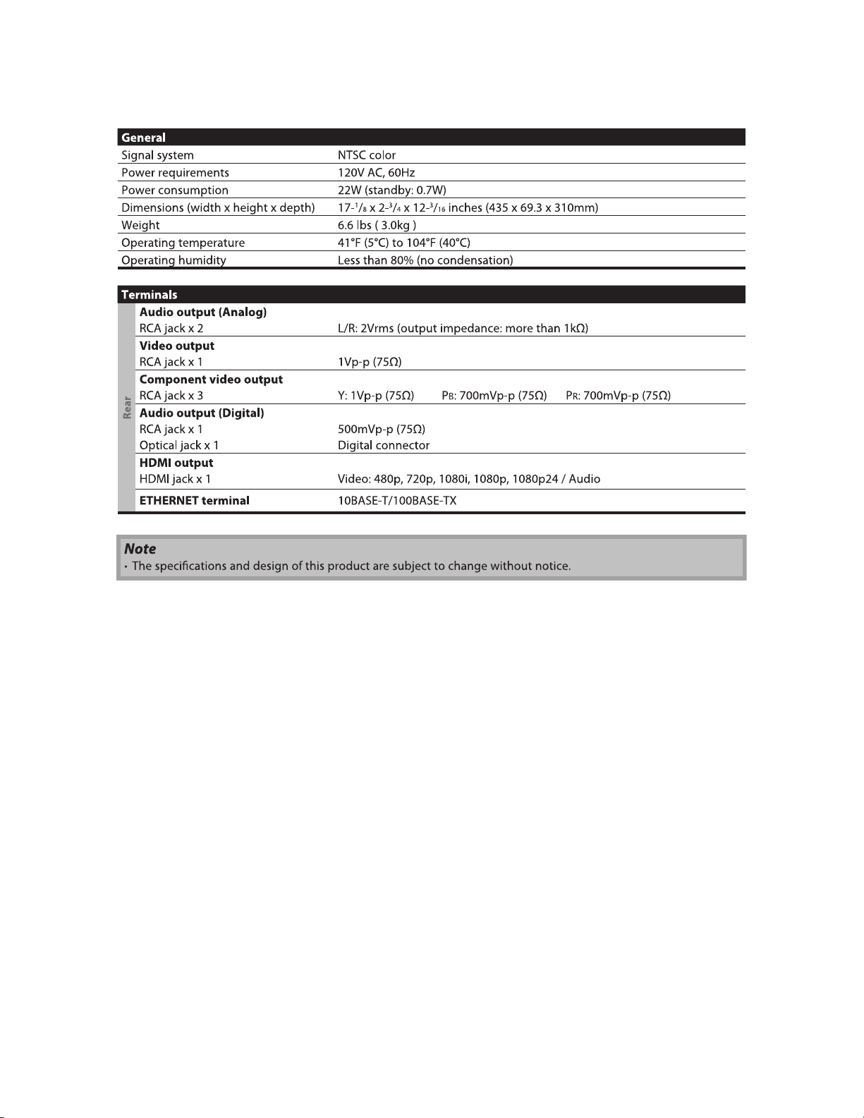
SPECIFICATIONS
1-1-1 E5K55SP
Page 4

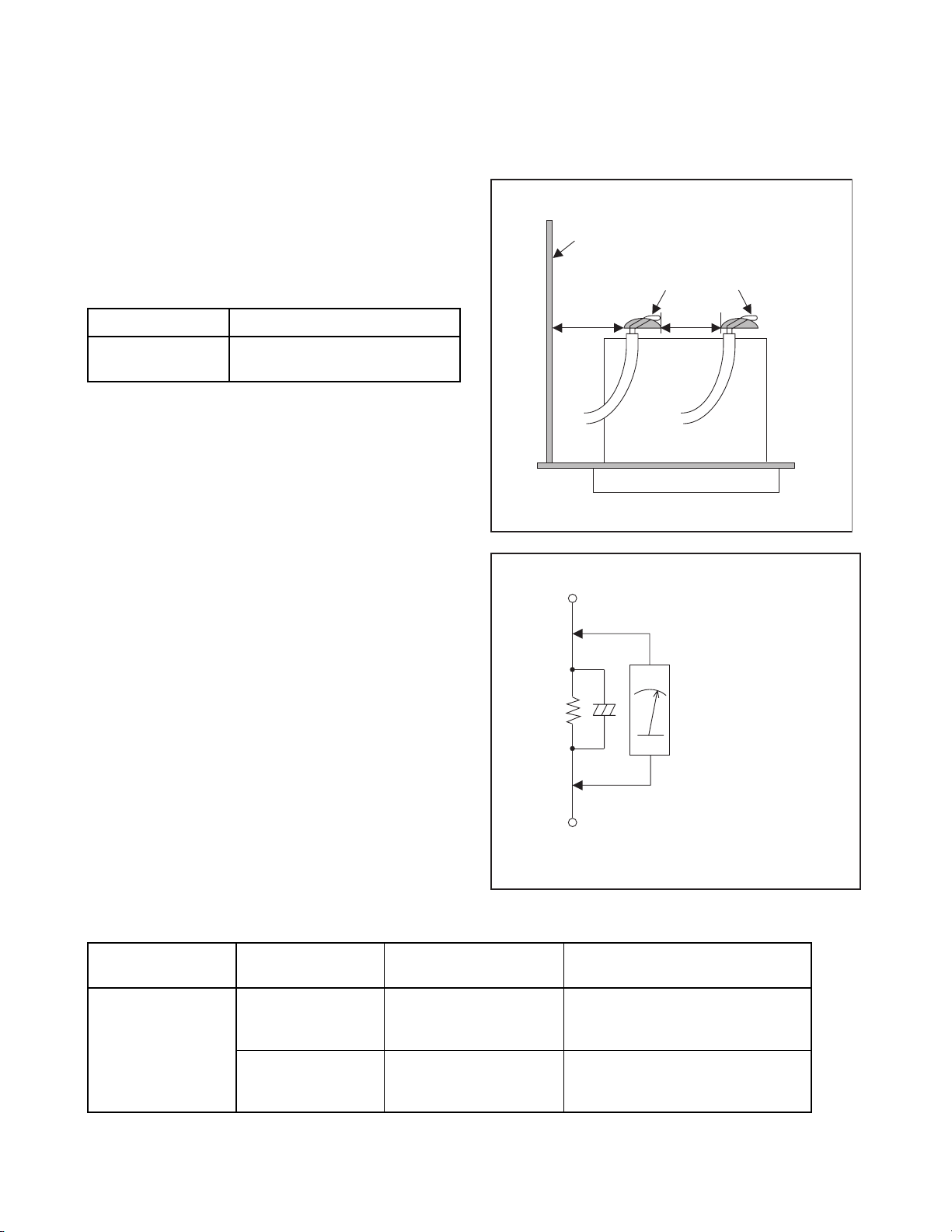
LASER BEAM SAFETY PRECAUTIONS
This BD player uses a pickup that emits a laser beam.
Do not look directly at the laser beam coming
from the pickup or allow it to strike against your
skin.
The laser beam is emitted from the location shown in the figure. When checking the laser diode, be sure to keep
your eyes at least 30 cm away from the pickup lens when the diode is turned on. Do not look directly at the laser
beam.
CAUTION: Use of controls and adjustments, or doing procedures other than those specified herein, may result in
hazardous radiation exposure.
Drive Mechanism Assembly
Laser Beam Radiation
Laser Pickup
Turntable
Location: Inside Top of BD mechanism.
1-2-1 B2NLBSP
Page 5

IMPORTANT SAFETY PRECAUTIONS
Product Safety Notice
Some electrical and mechanical parts have special
safety-related characteristics which are often not
evident from visual inspection, nor can the protection
they give necessarily be obtained by replacing them
with components rated for higher voltage, wattage,
etc. Parts that have special safety characteristics are
identified by a # on schematics and in parts lists. Use
of a substitute replacement that does not have the
same safety characteristics as the recommended
replacement part might create shock, fire, and/or other
hazards. The Product’s Safety is under review
continuously and new instructions are issued
whenever appropriate. Prior to shipment from the
factory, our products are carefully inspected to confirm
with the recognized product safety and electrical
codes of the countries in which they are to be sold.
However, in order to maintain such compliance, it is
equally important to implement the following
precautions when a set is being serviced.
Precautions during Servicing
A. Parts identified by the # symbol are critical for
safety. Replace only with part number specified.
B. In addition to safety, other parts and assemblies
are specified for conformance with regulations
applying to spurious radiation. These must also be
replaced only with specified replacements.
Examples: RF converters, RF cables, noise
blocking capacitors, and noise blocking filters, etc.
C. Use specified internal wiring. Note especially:
1) Wires covered with PVC tubing
2) Double insulated wires
3) High voltage leads
D. Use specified insulating materials for hazardous
live parts. Note especially:
1) Insulation tape
2) PVC tubing
3) Spacers
4) Insulators for transistors
E. When replacing AC primary side components
(transformers, power cord, etc.), wrap ends of
wires securely about the terminals before
soldering.
F. Observe that the wires do not contact heat
producing parts (heat sinks, oxide metal film
resistors, fusible resistors, etc.).
G. Check that replaced wires do not contact sharp
edges or pointed parts.
H. When a power cord has been replaced, check that
5 - 6 kg of force in any direction will not loosen it.
I. Also check areas surrounding repaired locations.
J. Be careful that foreign objects (screws, solder
droplets, etc.) do not remain inside the set.
K. When connecting or disconnecting the internal
connectors, first, disconnect the AC plug from the
AC outlet.
1-3-1 BDN_ISP
Page 6
Safety Check after Servicing
Examine the area surrounding the repaired location for damage or deterioration. Observe that screws, parts, and
wires have been returned to their original positions. Afterwards, do the following tests and confirm the specified
values to verify compliance with safety standards.
1. Clearance Distance
When replacing primary circuit components, confirm
specified clearance distance (d) and (d’) between
soldered terminals, and between terminals and
surrounding metallic parts. (See Fig. 1)
Table 1: Ratings for selected area
Chassis or Secondary Conductor
Primary Circuit
AC Line Voltage Clearance Distance (d), (d’)
120 V
Note: This table is unofficial and for reference only. Be
sure to confirm the precise values.
≥ 3mm(d)
≥ 4mm(d’)
2. Leakage Current Test
Confirm the specified (or lower) leakage current
between B (earth ground, power cord plug prongs) and
externally exposed accessible parts (RF terminals,
antenna terminals, video and audio input and output
terminals, microphone jacks, earphone jacks, etc.) is
lower than or equal to the specified value in the table
below.
Measuring Method (Power ON):
Insert load Z between B (earth ground, power cord plug
prongs) and exposed accessible parts. Use an AC
voltmeter to measure across the terminals of load Z.
See Fig. 2 and the following table.
d' d
Exposed Accessible Part
Z
One side of
B
Power Cord Plug Prongs
Fig. 1
AC Voltmeter
(High Impedance)
Table 2: Leakage current ratings for selected areas
AC Line Voltage Load Z Leakage Current (i)
2kΩ RES.
Connected in
parallel
120 V
50kΩ RES.
Connected in
parallel
Note:This table is unofficial and for reference only. Be sure to confirm the precise values.
i≤0.7mA AC Peak
i≤2mA DC
i≤0.7mA AC Peak
i≤2mA DC
1-3-2 BDN_ISP
One side of power cord plug
prongs (B) to:
RF or
Antenna terminals
A/V Input, Output
Fig. 2
Page 7
STANDARD NOTES FOR SERVICING
Circuit Board Indications
1. The output pin of the 3 pin Regulator ICs is
indicated as shown.
To p Vi e w
Out
2. For other ICs, pin 1 and every fifth pin are
indicated as shown.
Pin 1
3. The 1st pin of every male connector is indicated as
shown.
Pin 1
Input
In
Bottom View
5
10
Pb (Lead) Free Solder
When soldering, be sure to use the Pb free solder.
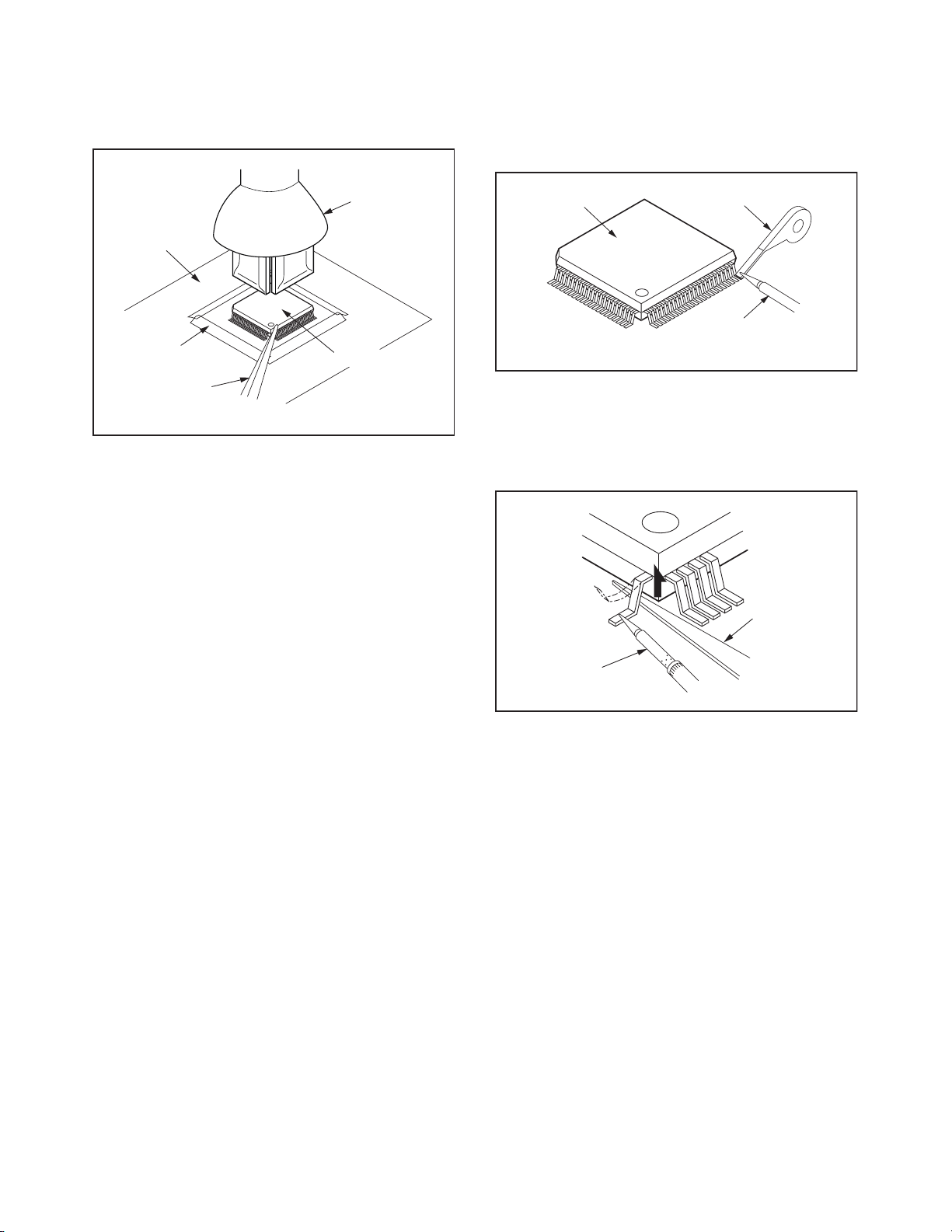
How to Remove / Install Flat Pack-IC
1. Removal
With Hot-Air Flat Pack-IC Desoldering Machine:
1. Prepare the hot-air flat pack-IC desoldering
machine, then apply hot air to the Flat Pack-IC
(about 5 to 6 seconds). (Fig. S-1-1)
Fig. S-1-1
Instructions for Connectors
1. When you connect or disconnect the FFC (Flexible
Foil Connector) cable, be sure to first disconnect
the AC cord.
2. FFC (Flexible Foil Connector) cable should be
inserted parallel into the connector, not at an
angle.
FFC Cable
Connector
CBA
* Be careful to avoid a short circuit.
2. Remove the flat pack-IC with tweezers while
applying the hot air.
3. Bottom of the flat pack-IC is fixed with glue to the
CBA; when removing entire flat pack-IC, first apply
soldering iron to center of the flat pack-IC and heat
up. Then remove (glue will be melted). (Fig. S-1-6)
4. Release the flat pack-IC from the CBA using
tweezers. (Fig. S-1-6)
CAUTION:
1. The Flat Pack-IC shape may differ by models. Use
an appropriate hot-air flat pack-IC desoldering
machine, whose shape matches that of the Flat
Pack-IC.
2. Do not supply hot air to the chip parts around the
flat pack-IC for over 6 seconds because damage
to the chip parts may occur. Put masking tape
around the flat pack-IC to protect other parts from
damage. (Fig. S-1-2)
1-4-1 BDN_SN
Page 8
3. The flat pack-IC on the CBA is affixed with glue, so
be careful not to break or damage the foil of each
pin or the solder lands under the IC when
removing it.
With Soldering Iron:
1. Using desoldering braid, remove the solder from
all pins of the flat pack-IC. When you use solder
flux which is applied to all pins of the flat pack-IC,
you can remove it easily. (Fig. S-1-3)
CBA
Masking
Ta pe
Tweezers
Hot-air
Flat Pack-IC
Desoldering
Machine
Flat Pack-IC
Fig. S-1-2
Flat Pack-IC
Desoldering Braid
Soldering Iron
Fig. S-1-3
2. Lift each lead of the flat pack-IC upward one by
one, using a sharp pin or wire to which solder will
not adhere (iron wire). When heating the pins, use
a fine tip soldering iron or a hot air desoldering
machine. (Fig. S-1-4)
Sharp
Pin
Fine Tip
Soldering Iron
3. Bottom of the flat pack-IC is fixed with glue to the
CBA; when removing entire flat pack-IC, first apply
soldering iron to center of the flat pack-IC and heat
up. Then remove (glue will be melted). (Fig. S-1-6)
4. Release the flat pack-IC from the CBA using
tweezers. (Fig. S-1-6)
Fig. S-1-4
1-4-2 BDN_SN
Page 9
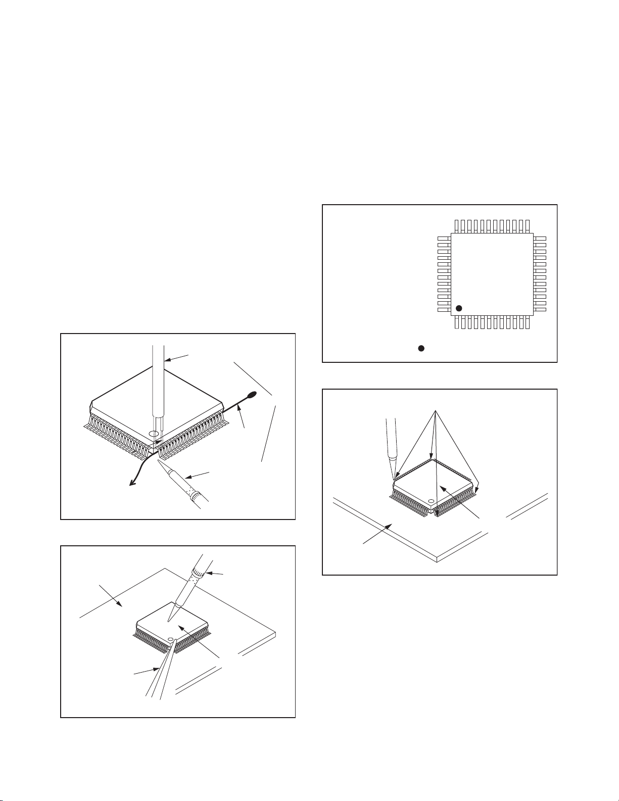
With Iron Wire:
1. Using desoldering braid, remove the solder from
all pins of the flat pack-IC. When you use solder
flux which is applied to all pins of the flat pack-IC,
you can remove it easily. (Fig. S-1-3)
2. Affix the wire to a workbench or solid mounting
point, as shown in Fig. S-1-5.
3. While heating the pins using a fine tip soldering
iron or hot air blower, pull up the wire as the solder
melts so as to lift the IC leads from the CBA
contact pads as shown in Fig. S-1-5.
4. Bottom of the flat pack-IC is fixed with glue to the
CBA; when removing entire flat pack-IC, first apply
soldering iron to center of the flat pack-IC and heat
up. Then remove (glue will be melted). (Fig. S-1-6)
5. Release the flat pack-IC from the CBA using
tweezers. (Fig. S-1-6)
Note: When using a soldering iron, care must be
taken to ensure that the flat pack-IC is not
being held by glue. When the flat pack-IC is
removed from the CBA, handle it gently
because it may be damaged if force is applied.
Hot Air Blower
2. Installation
1. Using desoldering braid, remove the solder from
the foil of each pin of the flat pack-IC on the CBA
so you can install a replacement flat pack-IC more
easily.
2. The “●” mark on the flat pack-IC indicates pin 1.
(See Fig. S-1-7.) Be sure this mark matches the
pin 1 on the PCB when positioning for installation.
Then presolder the four corners of the flat pack-IC.
(See Fig. S-1-8.)
3. Solder all pins of the flat pack-IC. Be sure that
none of the pins have solder bridges.
Example :
Pin 1 of the Flat Pack-IC
is indicated by a " " mark.
Fig. S-1-7
To Solid
Mounting Point
CBA
Tweezers
Iron Wire
Soldering Iron
Fig. S-1-5
Fine Tip
Soldering Iron
Flat Pack-IC
or
Presolder
Flat Pack-IC
CBA
Fig. S-1-8
Fig. S-1-6
1-4-3 BDN_SN
Page 10

Instructions for Handling Semiconductors
Electrostatic breakdown of the semi-conductors may
occur due to a potential difference caused by
electrostatic charge during unpacking or repair work.
1. Ground for Human Body
Be sure to wear a grounding band (1 MΩ) that is
properly grounded to remove any static electricity that
may be charged on the body.
2. Ground for Workbench
Be sure to place a conductive sheet or copper plate
with proper grounding (1 MΩ) on the workbench or
other surface, where the semi-conductors are to be
placed. Because the static electricity charge on
clothing will not escape through the body grounding
band, be careful to avoid contacting semi-conductors
with your clothing.
<Incorrect>
<Correct>
1MΩ
CBA
Grounding Band
1MΩ
CBA
Conductive Sheet or
Copper Plate
1-4-4 BDN_SN
Page 11

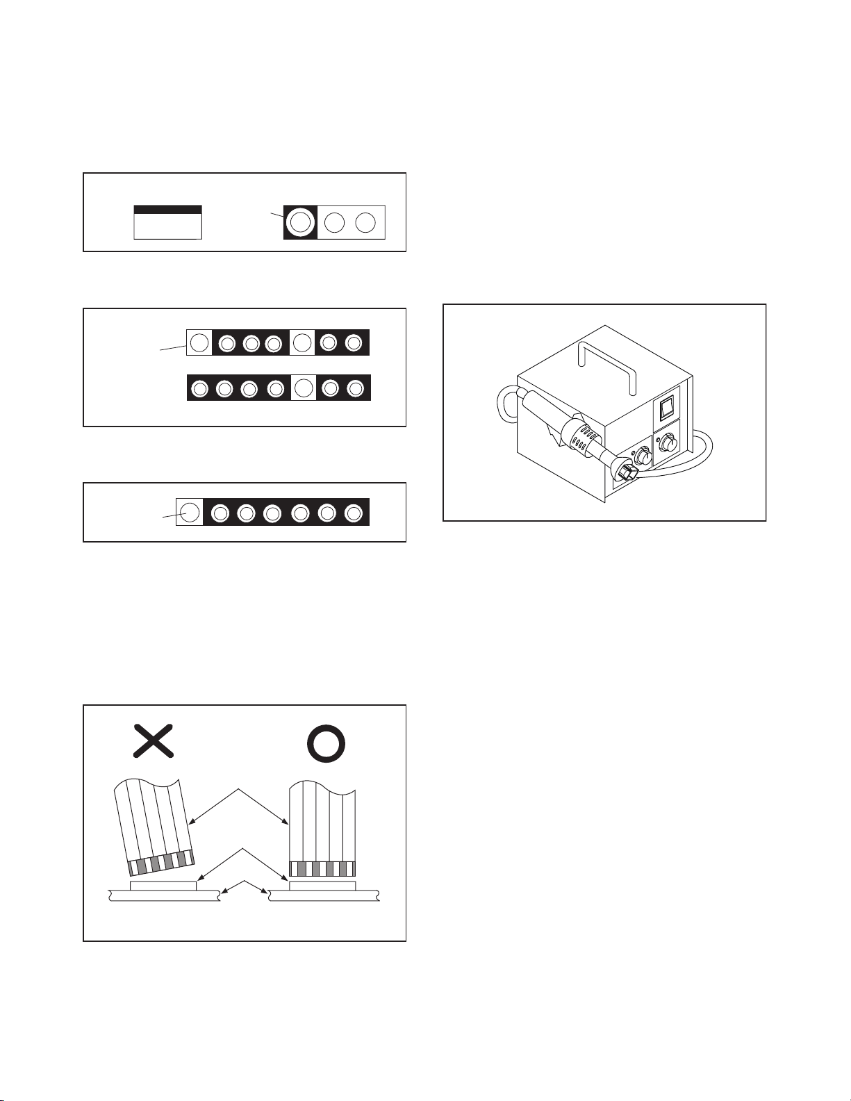
CABINET DISASSEMBLY INSTRUCTIONS
1. Disassembly Flowchart
This flowchart indicates the disassembly steps to gain
access to item(s) to be serviced. When reassembling,
follow the steps in reverse order. Bend, route, and
dress the cables as they were originally.
[1] Top Cover
[2] Front Assembly
[5] RS232C CBA
[6] BD Main CBA &
BD Mechanism Assembly
[7] SD-A CBA
[8] SD-B CBA
[9] SD-C CBA
[10] Rear Panel
[12] AV CBA
[13] Power Holder
[3] Front CBA
[4] Power SW CBA
[14] Shield Bracket
[15] SD PCB Bracket
[11] Motor DC Fan
2. Disassembly Method
ID/
Loc.
No.
Part
Fig.
No.
[1] Top Cover D1 9(S-1) ---
*5(L-1), *3(L-2),
D2
*5(S-2) *CN2002,
*CN3001
[2]
Front
Assembly
[3] Front CBA D2 --------------- ---
Power SW
[4]
[5]
CBA
RS232C
CBA
D2 --------------- ---
D3 2(S-3), *CN2006 ---
(S-4), 2(S-5), 4(S-6),
BD Main
CBA & BD
[6]
Mechanism
Assembly
2(S-7), 4(S-8),
*CN6001, *CN7101,
D3
*CN7601, Main PCB
Earth Plate, Front
Shield
[7] SD-A CBA D3 Desolder --[8] SD-B CBA D3 Desolder --[9] SD-C CBA D3 --------------- ---
[10] Rear Panel D4
2(S-9), 4(S-10),
2(S-11), (S-12)
Removal
Remove/*Unhook/
Unlock/Release/
Unplug/Desolder
Note
1
2
---
ID/
Loc.
No.
[11]
Part
Motor DC
Fan
Remove/*Unhook/
Fig.
No.
Unlock/Release/
Unplug/Desolder
Note
D4 *CN2004, Fan Holder ---
[12] AV CBA D5 5(S-13) ---
Removal
Power
[13]
[14]
[15]
↓
(1)
Holder
Shield
Bracket
SD PCB
Bracket
↓
(2)
D5 (S-14) ---
D5 4(S-15) ---
D5 (S-16) ---
↓
(3)
↓
(4)
(5)
↓
Note:
(1) Identification (location) No. of parts in the figures
(2) Name of the part
(3) Figure Number for reference
(4) Identification of parts to be removed, unhooked,
unlocked, released, unplugged, unclamped, or
desoldered.
P = Spring, L = Locking Tab, S = Screw,
CN = Connector
* = Unhook, Unlock, Release, Unplug, or Desolder
e.g. 2(S-2) = two Screws (S-2),
2(L-2) = two Locking Tabs (L-2)
(5) Refer to “Reference Notes.”
Reference Notes
1. CAUTION 1: Locking Tabs (L-1) and (L-2) are
fragile. Be careful not to break them.
2. The BD Main CBA & BD Mechanism Assembly
is adjusted as a unit at factory. Therefore, do
not disassemble it. Replace the BD Main CBA
& BD Mechanism Assembly as a unit.
1-5-1 E5K55DC
Page 12
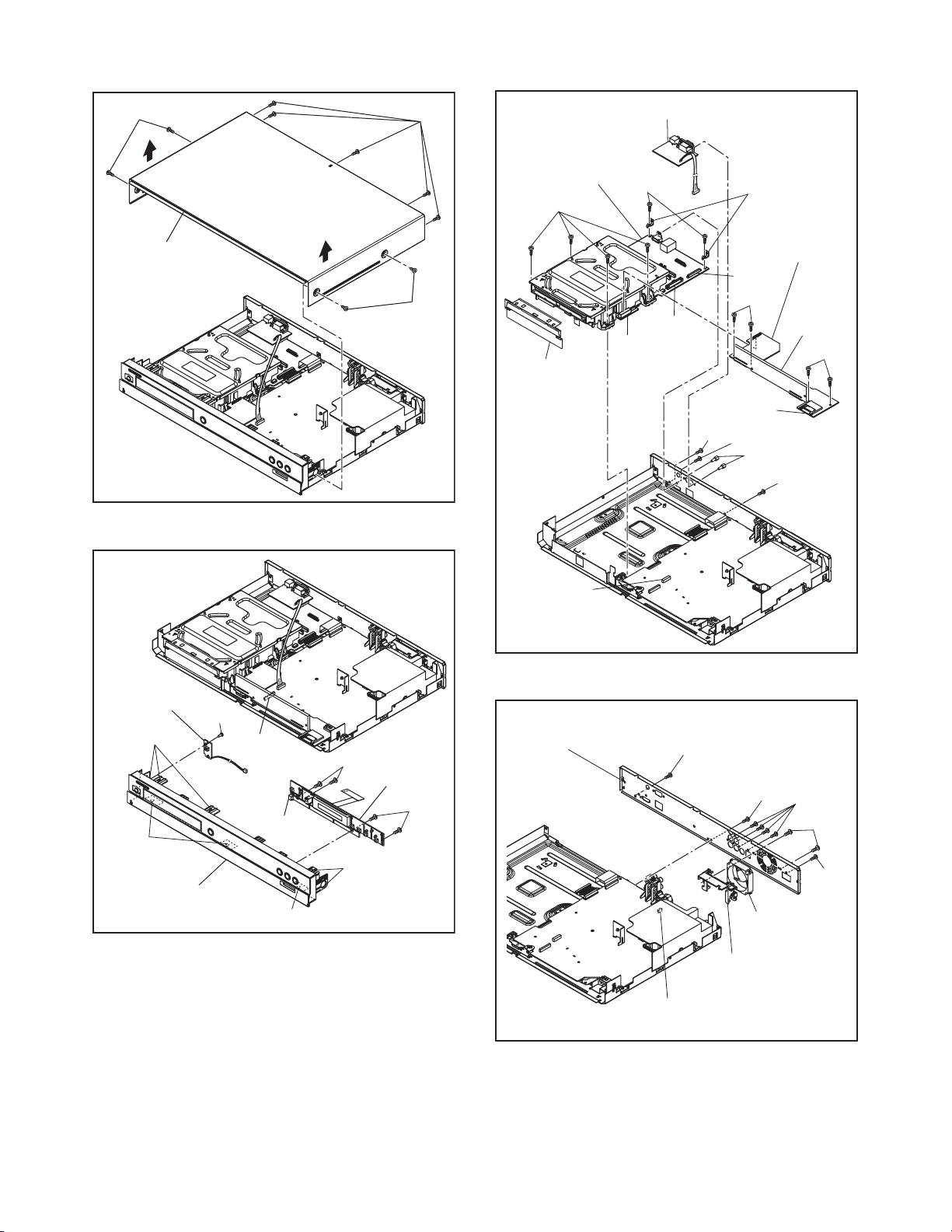
(S-1)
(S-1)
[6] *BD Main
CBA & BD
Mechanism
Assembly
(S-6)
[5] RS232C-CBA
(S-7)
Main PCB
Earth Plate
[1] Top Cover
[4] Power SW
CBA
(L-1)
(L-2)
(S-2)
CN2002
CN3001
(S-2)
[3] Front CBA
(S-1)
Fig. D1
(S-2)
CN6001
CN7601
Front Shield
CN2006
* See Reference Notes 2.
[10] Rear Panel
(S-9)
(S-5)
[7] SD-A CBA
CN7101
(S-8)
[9] SD-C
CBA
(S-4)
(S-3)
(S-9)
[8] SD-B
CBA
(S-8)
(S-5)
Fig. D3
(S-10)
(S-11)
[2] Front Assembly
(L-2)
(L-1)
Fig. D2
(S-12)
[11] Motor
DC Fan
Fan Holder
CN2004
Fig. D4
1-5-2 E5K55DC
Page 13

[12] AV CBA
[14] Shield
Bracket
(S-13)
(S-15)
[15] SD PCB
Bracket
[13] Power Holder
(S-14)
(S-16)
Fig. D5
1-5-3 E5K55DC
Page 14

3. How to Eject Manually
1. Remove the Top Cover.
2. Insert a screwdriver, etc. into the Hole A straightly so that the Portion A is pushed.
3. Pull the tray out manually and remove a disc.
Portion A
Screwdriver,
hexagon wrench
1-5-4 E5K55DC
Page 15
HOW TO INITIALIZE THE BLU-RAY DISC PLAYER
To put the program back at the factory-default,
initialize the BD player as the following procedure.
1. Turn the power on.
2. Remove the disc on the tray and close the tray.
3. Press [1], [2], [3], [4], and [DISPLAY] buttons on
the remote control unit in that order.
Fig. a appears on the screen.
"
" differ depending on the models.
*******
Version Info
F/W Name
Version
Region
: *******
: *.***
: *-*
EXIT <POWER>EEPROM CLEAR <STOP>
Fig. a
4. Press [ C ] button on the remote control unit.
Fig. b appears on the screen and Fig. c appears
on the VFD.
"
" differ depending on the models.
*******
Version Info
F/W Name
Version
Region
EEPROM CLEAR : OK
: *******
: *.***
: *-*
EXIT <POWER>EEPROM CLEAR <STOP>
Fig. b
Fig. c
5. To exit this mode, press [ON/STANDBY] button.
1-6-1 E5K50INT
Page 16
FIRMWARE RENEWAL MODE
Note: The file extension of the available firmware is
“b20”.
1. Turn the power on and remove the disc on the tray
and close the tray.
2. To put the BD player into version up mode, press
[9], [8], [7], [6], and [POP UP MENU/MENU]
buttons on the remote control unit in that order.
The tray will open automatically.
Fig. a appears on the screen and Fig. b appears
on the VFD.
"
" differs depending on the models.
*******
F/W VERSION UP MODE F/W Name: ******* Ver. *.***
Please insert a Disc
for F/W Version Up
Fig. a Version Up Mode Screen
Fig. b VFD in Version Up Mode
3. Load the disc for version up.
4. The BD player enters the F/W version up mode
automatically. Fig. c appears on the screen and
Fig. d appears on the VFD. Make sure to insert the
proper F/W for the state of this model.
"
" differs depending on the models.
*******
F/W VERSION UP MODE F/W Name: ******* Ver. *.***
1. ALL
(*1)
Ver. *.*** ************A*.b20
Now Loading...
The appearance shown in (*1) of Fig. c is
described as follows:
No. Appearance State
1 Now Loading... Loading the disc
Sending files into the
2 Reading...
memory.
After reading, automatically
the tray opens.
Writing new version data,
3 See FL Display
the progress will be displayed
as shown in Fig. e.
Fig. e VFD in Vresion Up Mode
5. After programming is finished, the checksum on
the VFD (Fig. f).
Fig. f
VFD upon Finishing the Programming Mode (Example)
Checksum appears on the VFD then the tray will
open automatically. Remove the disc on the tray.
At this time, no button is available.
6. Unplug the AC cord from the AC outlet. Then plug
it again.
7. Turn the power on.
8. Press [1], [2], [3], [4], and [DISPLAY] buttons on
the remote control unit in that order.
Fig. g appears on the screen.
"
" differ depending on the models.
*******
Version Info
F/W Name
Version
Region
: *******
: *.***
: *-*
EXIT : POWER
Fig. c Programming Mode Screen (Example)
Fig. d VFD in Programming Mode (Example)
EXIT <POWER>EEPROM CLEAR <STOP>
Fig. g
1-7-1 E5K50FW
Page 17

9. Press [ C ] button on the remote control unit.
Fig. h appears on the screen and Fig. i appears on
the VFD.
"
" differ depending on the models.
*******
Version Info
F/W Name
Version
Region
: *******
: *.***
: *-*
How to Verify the Firmware Version
1. Turn the power on.
2. Remove the disc on the tray and close the tray.
3. Press [1], [2], [3], [4], and [DISPLAY] buttons on
the remote control unit in that order.
Fig. j appears on the screen.
"
" differ depending on the models.
*******
Version Info
EEPROM CLEAR : OK
EXIT <POWER>EEPROM CLEAR <STOP>
Fig. h
Fig. i
10. To exit this mode, press [ON/STANDBY] button.
F/W Name
Version
Region
: *******
: *.***
: *-*
EXIT <POWER>EEPROM CLEAR <STOP>
Fig. j
4. To exit this mode, press [ON/STANDBY] button.
1-7-2 E5K50FW
Page 18

BLOCK DIAGRAMS
System Control Block Diagram
TO POWER SUPPLY
TO VIDEO
BLOCK DIAGRAM
BLOCK DIAGRAM
TO AUDIO
BLOCK DIAGRAM
EV+5V
SENSOR
REMOTE
RS3000
VFD
FRONT CBA
19 20 21 22
FL3000
KEY
SWITCH
Q3000
CN3001
POWER-LED
1
KEY-1
2
WX3000
1
2
D3007
POWER
POWER
SW3007
POWER SW CBA
(SUB MICRO CONTROLLER)
IC2000
MUTE1
IC2001
MUTE2
21MUTE1
22MUTE2
RESET
14
RESET
EV+3.3V
X2000
PWSW1
OSC1
8
PWSW2
A33-PW-CONT
4
PWSW137PWSW2
OSC2
9
8MHz
X'TAL
FL-SW
FAN-LOCK
FAN-CONT1
31
32
63
25FAN-CONT1
FL-SW
FAN-LOCK
A33-PW-CONT
28 CEC-IN
SWITCHING
Q2620, Q2621
BUFFER
Q2619
Q2618
CN2001
FAN-CONT2
26FAN-CONT2
CEC-OUT
30
BUFFER
AUDIO-MUTE
24AUDIO-MUTE
56
POWER-LED
SUB-TXD
SUB-RXD
15
16
18 16FL-SDA
CN2002 CN3000
33
FL-SDA
SYS-RESET
3
16 14FL-STB
17 15FL-SCL
49
34
FL-SCL
FL-STB
-LED
POWER
64KEY-1
97REMOTE
53
15 13FL-RESET
62
27
50
KEY-1
REMOTE
FL-RESET
RS232C-RXD
45 RS232C-TXD
46
CN2006
AV CBA
TX(+)
123
JK6401
ETHERNET JACK
12
IC6401
(ETHERNET INTERFACE)
39
TX(-)
11
38
36
RX(+)
10
35
RX(-)
6
9
ETHERNET
INTERFACE
33
REMOTE
RS232C-TXD
RS232C-RXD
55
33
22
CN5501
BUFFER
Q5551,Q5552
3
4
IC5550
PHOTO
COUPLER
1
11
12
2
CN7101
JK7501
22CEC
13
CEC
IC6903 (EEPROM)
88SUB-TXD
99SYS-RESET
77SUB-RXD
CN7101 CN2001
Q6702
MII-TXD3
G5
IC6701
Q6701
RESET
2 1
RS232C CBA
V32
U34
TXD1
RXD1
SCL0
IC6001
(MAIN MICRO CONTROLLER)
V31
SDA0
W30
SCL
SDA
5
6
MII-RXD1
MII-RXD0
MII-RXCLK
J4
MII-RXD3
MII-RXD2
J2J1J3
K2
AE32
XTRST
MII-TXD0
MII-TXCLK
MII-TXD1
H5
H4
G4
T34
XRST
MII-TXD2
F4
BD MAIN CBA
28
23
22
21
20
1-8-1
P-ON+1.8V
RS232C
IC5500
INTERFACE
CN5500
RS232C-
CONNECTOR
RS232C
I/F
13
14
2TXD
3RXD
JK5550
REMOTE
-IN
E5K55BLS
Page 19

Digital Signal Process 1 Block Diagram
VIDEO SIGNAL AUDIO SIGNAL
TO DIGITAL SIGNAL
PROCESS 2 BLOCK
DIAGRAM
(IC6001)
BD+
CSS
AACS
STREAM
FE
DIGITAL
CONTROL
SIGNAL
PROCESS
COPY
PROTECT
CPRM
(MAIN MICRO CONTROLLER/DIGITAL SIGNAL PROCESS)
IC6001
B28
A28
20 SE02
18 SE01
MPX
IC201 (FRONT-END PROCESSOR)
97-100
ASENV
H34
59
WOB
MATRIX
102-105
G34
61 WBL
/LPP
868588
107-110
B34
C33
66
655453
RF
EQUALIZER
RF
GENERATOR
87
SCLK1
SD ATA 1
TRACKING-CONTROL
FOCUS1-CONTROL
A24
7 6
FOCUS 1
ACTUATOR
DRIVE
18
FOCUS2-CONTROL
D23
8 9
12
FOCUS 2
ACTUATOR
DRIVE
17
16
SD ATA 2
SD ATA 1
SCLK2
SCLK1
J34
J33
83 78 79
M31
M32
E23
IC604 (OP AMP)
1 2
22
TRACKING
IC603 (MOTOR DRIVE)
212019
ACTUATOR
DRIVE
COLLIMATE
IC602 (MOTOR DRIVE)
236
EXPA-CONTROL
EXPB-CONTROL
B22
D22
132310
LENS
MOTOR DRIVE
5
IC603 (MOTOR DRIVE)
32
SLED1-CONTROL
SLED2-CONTROL
D24
C24
4
30
SLED
MOTOR DRIVE
2
33
TRAY-OUT
TRAY-IN
INLIMIT
LOAD-CONTROL
C22
D21
E21
SPINDLE-CONTROL
B3
E24
SPINDLE-FG
B25
BD MAIN CBA
SPINDLE
MOTOR
DRIVE
4
12
13
LOADING
MOTOR DRIVE
1
14
15
10
IC601 (MOTOR DRIVE)
242119131415161718
CN101
A-D 21-24
E-H 26-29
RF(+) 17
BD MECHANISM
RF(-) 18
BDRF(+) 14
OEIC
(CD/DVD)
TRAY-OUT
CN603
V2
U3
W1
INLIMIT 4
TRAY-IN 1
INNER
SW
TRAY-IN
HU(+) 5
SPINDLE
HV(-) 8
HU(-) 6
MOTOR
HB(-) 11
HV(+) 7
HW(-) 10
HW(+) 9
E5K55BLD1
CN101
TD 3
TR 4
FD1 1
FR1 2
FR2 5
LASER
DIODE
FD2 6
DRIVE
EXPA(-) 7
EXPB(-) 8
EXPA(+) 9
EXPB(+) 10
SCLK2 38
SD ATA 2 4 0
BDRF(-) 15
OEIC
(BD)
CN601
SLD2(+) 4
SLD2(-) 3
SLED
CN602
SLD1(-) 1
LOAD(+) 5
LOADING
MOTOR
LOAD(-) 6
TRAY-OUT 2
SLD1(+) 2
MOTOR
1-8-2
Page 20

Digital Signal Process 2 Block Diagram
TO
VIDEO
BLOCK
DIAGRAM
SCL3
VIDEO
VIDEO SIGNAL AUDIO SIGNAL
C15
VIDEO-Pr/Cr
VIDEO-Y(I/P)
VIDEO-Pb/Cb
F17
B17
D18
VIDEO
DAC
PRMVS
PRMCLK
A2B6B5
CLK
VSYNC
PRMHS
PRMC(0-11)
A4,A8,A9,B4,B9,C5,C9,
C11,D8,D10,E10,E11
HSYNC
DIGITAL
SDA3
PRMY(0-11)
R33
U31
A3,A6,A7,B7,C4,C6,C7,
C8,D6,D9,E8,E12
SCL3
SDA3
VIDEO
OUT
2
3
SCL
SDA
IC6703
(CLOCK GENE.)
I/P CONVERTER
/SCALING
27MHz
X6701
1
CLOCK
789
E20
AL5
AL34
33M CLOCK
33M CLOCK
74M CLOCK
OSC
16
GENE.
10
A19
D20
27M CLOCK
768K CLOCK
TO
AUDIO
BLOCK
DAC-SCK
DAC-BCK
A12
DAC-LRCK
B13
D12
DIAGRAM
SPDIF
B12
MS1
DATA
A13
AC31
TO
VIDEO
BLOCK
DIAGRAM
MC
MD
HDMI-BCK
HDMI-MCK
HDMI-DATA0
HDMI-DATA1
E13
B10
HDMI-LRCK
HDMI-DATA2
HDMI-DATA3
HDMI-SPDIF
AUDIO
OUT
C14
B14
B11
A10
A11
D11
C12
C10
DIGITAL
IC6001 (MAIN MICRO CONTROLLER/DIGITAL SIGNAL PROCESS)
SD-A CBA
SD-B CBA
CN7601CN4001
11 6SDDAT0
CN4003
11 11SDDAT0
CN4102 CN4101
SD I/F
AF32,AG34,
SD DATA(0-3)
13 4SDDAT1
13 13SDDAT1
SDCLK
AH34
AH33,AJ34
116SDDAT2
314SDDAT3
98SDCLK
11SDDAT2
33SDDAT3
99SDCLK
MEDIA
PROCESSOR
FROM
DIGITAL
SIGNAL
PROCESS 1
BLOCK
DIAGRAM
(IC6001)
Java (BD-J)
(NAND FLASH MEMORY)
IC6902
MPEG-2
DiVX
VC-1
H.264
DECODER
HD (TS)
ED (0-7)
NAND FLASH
MEMORY (64M x 8bit)
SD (PS)
C0DQ (0-31)
(DDR2 SDRAM)
IC6501,IC6502
MEMORY
I/F
C0A (0-12)
DDR2 SDRAM
(1Gbit )
C1DQ (0-31)
(DDR2 SDRAM)
IC6601,IC6602
C1A (0-12)
DDR2 SDRAM
(512Mbit)
115SDDAT2
313SDDAT3
97SDCLK
11 5SDDAT0
13 3SDDAT1
CN4004
BD MAIN CBA
SD-C CBA
CN4002
SD
CARD
SLOT
1-8-3
E5K55BLD2
Page 21

Video Block Diagram
VIDEO OUT
(COMPOSITE)
JK2200
VIDEO-Y
JK2300
OUT
VIDEO-Pb/Cb
OUT
VIDEO-Pr/Cr
OUT
DDC DATA
DDC CLOCK
HOT PLUG
DETECT
191516
HDMI-CONNECTOR
JK7501
T.M.D.S DATA2-
T.M.D.S DATA2+
T.M.D.S DATA1-
T.M.D.S DATA1+
31649
T.M.D.S DATA0-
T.M.D.S DATA0+
7
T.M.D.S CLOCK+
T.M.D.S CLOCK-
10
12
VIDEO SIGNAL AUDIO SIGNAL
AV CBABD MAIN CBA
75Ω
DRIVER
2dB
AMP
LPF 25
4dB
AMP
IC2300 (VIDEO DRIVER)
3
C2323
6.75MHz
75Ω
2dB
LPF
4dB
8 20
DRIVER
AMP
AMP
17
75Ω
DRIVER
2dB
AMP
LPF
13.5/37MHz
13.5/37MHz
4dB
AMP
10
CN2001CN7101
15
75Ω
DRIVER
2dB
AMP
LPF
4dB
AMP
12
13.5/37MHz
MUTE1
2
MUTE1
MUTE2
TO SYSTEM CONTROL
BLOCK DIAGRAM
MUTE2
13
118
DDC
AUTHENT
/CATION
KEY
EXCHANGE
REGISTER
IIC
I/F
113
116
CLK
121
IC7501 (HDMI INTERFACE)
I/F
VS
83
23251921151713
120
119
HS
84
50,51,53-57,59,
87,88,90,91
TMDS
SERIALIZER
TMDS
ENCODER
HDCP
CIPHER/
ENCRYPTOR
AV
CONTROLLER
VIDEO
I/F
70-73,75-78,
92,94,102,103
11
AUDIO
I/F
46454442413936
35
16 16VIDEO-Y(I/P)
14 14VIDEO
VIDEO
VIDEO-Y(I/P)
18 18VIDEO-Pb/Cb
20 20VIDEO-Pr/Cr
VIDEO-Pb/Cb
VIDEO-Pr/Cr
TO DIGITAL
SIGNAL
1-8-4
PROCESS 2
BLOCK DIAGRAM
SCL3
SDA3
PRMCLK
PRMVS
PRMHS
PRMC(0-11)
PRMY(0-11)
HDMI-DATA0
HDMI-DATA1
HDMI-DATA2
HDMI-DATA3
HDMI-MCK
HDMI-BCK
HDMI-LRCK
HDMI-SPDIF
TO DIGITAL
SIGNAL
PROCESS 2
BLOCK DIAGRAM
E5K55BLV
Page 22

Audio Block Diagram
AUDIO SIGNAL
AUDIO(L)-
OUT
JK2200 (REAR)
MUTE-ON
Q2203
DRIVE
Q2200
7
AUDIO(R)-
Q2202
Q2201
1
OUT
MUTE-ON
DRIVE
DIGITAL
JK2100
(REAR)
BUFFER
Q2100
AUDIO OUT
(COAXIAL)
DIGITAL
AUDIO OUT
(OPTICAL)
JK2400 (REAR)
AV CBABD MAIN CBA
IC2200
(OP AMP)
CN7101 CN2001
(L-CH)
6
24 24AUDIO(L)
22 22AUDIO(R)
14
15
(R-CH)
2
55SPDIF
26 26AUDIO(L)-MUTE
25 25AUDIO(R)-MUTE
1
R-CH
MUTE
L-CH
MUTE
AUDIO-MUTE
TO SYSTEM CONTROL
BLOCK DIAGRAM
16
IC7001
(AUDIO D/A CONVERTER)
AUDIO
345
MCMDDAC-SCK
DAC-BCK
TO DIGITAL
DAC
827
DAC-LRCK
MS1
SIGNAL
PROCESS 2
BLOCK DIAGRAM
6
DATA
1-8-5
SPDIF
E5K55BLA
Page 23

Power Supply Block Diagram
TO BD MAIN
CBA
(CN6001)
AUDIO+3.3V
P-ON+1.2V
P-ON+1.8V
2 P-ON+5V(1)
5,6 P-ON+3.3V
9-11
17-20
23 P-ON+5V(2)
3,4 P-ON+10.5V
CN2000
NOTE:
The voltage for parts in hot circuit is measured using
hot GND as a common terminal.
EV+5V
EV+3.3V
TO SYSTEM
CONTROL
BLOCK
DIAGRAM
P-ON+3.3VF1F2
P-ON+5V
FL
FL-SW
PWSW2
FAN-LOCK
FAN-CONT1
FAN-CONT2
PWSW1
A33-PW-CONT
Q2611
Q2013
Q2610
P-ON+14.5V-B
P-ON+14.5V-A
CONTROL
(HIGH SPEED)
FAN
Q2000,Q2001
CN2004
FAN
FAN
Q2002,Q2003
"Ce symbole reprèsente un fusible à fusion rapide."
"This symbol means fast operating fuse."
CAUTION !
For continued protection against fire hazard,
replace only with the same type fuse.
ATTENTION : Pour une protection continue les risqes
d'Incele n'utiliser que des fusible de même type.
Risk of fire-replace fuse as marked.
F
A V
11
CONTROL
2FAN-LOCK
FAN-VCC 1
Q2204,Q2205
(LOW SPEED)
+3.3V
Q1011
12
SW+3.3V
REG.
15
Q2603
SW+14.5V
13
SW+10.5V
Q2607
Q2602
Q2601
Q2606
SW+5V
Q2608, Q2609
LIMIT
CURRENT
Q2604
SW+5V
Q2605
REG.
+3.3V
IC2600
Q2600
IC2602
REG.
+1.8V
+1.2V
IC2601
REG.
Q2012 Q2101
Q2014
Q2612
AV CBA
Q2613
COLD
REG.
9
10
16
14
1
SHUNT
2
T1001
2
BRIDGE
RECTIFIER
D1001 - D1004
LINE
FILTER
L1001
F
F1001
2A 250V
A V
HOT CIRCUIT. BE CAREFUL.
CAUTION !
Fixed voltage (or Auto voltage selectable) power supply circuit is used in this unit.
If Main Fuse (F1001) is blown , check to see that all components in the power supply
circuit are not defective before you connect the AC plug to the AC power supply.
Otherwise it may cause some components in the power supply circuit to fail.
AC1001
AC CORD
4
Q1003
5
)
SWITCHING
CONTROL
SWITCHING CONTROL
IC1001
(
2
1
VDD
3
6
1-8-6
4
IC1003
ERROR
7
6
VOLTAGE DET
3
IC1011
ERROR
VOLTAGE DET
HOT
E5K55BLP
Page 24

SCHEMATIC DIAGRAMS / CBA AND TEST POINTS
Standard Notes
WARNING
Many electrical and mechanical parts in this chassis
have special characteristics. These characteristics
often pass unnoticed and the protection afforded by
them cannot necessarily be obtained by using
replacement components rated for higher voltage,
wattage, etc. Replacement parts that have these
special safety characteristics are identified in this
manual and its supplements; electrical components
having such features are identified by the mark “#” in
the schematic diagram and the parts list. Before
replacing any of these components, read the parts list
in this manual carefully. The use of substitute
replacement parts that do not have the same safety
characteristics as specified in the parts list may create
shock, fire, or other hazards.
Notes:
1. Do not use the part number shown on these
drawings for ordering. The correct part number is
shown in the parts list, and may be slightly
different or amended since these drawings were
prepared.
2. All resistance values are indicated in ohms
(K = 10
3. Resistor wattages are 1/4W or 1/6W unless
otherwise specified.
4. All capacitance values are indicated in µF
(P = 10
5. All voltages are DC voltages unless otherwise
specified.
3
, M = 106).
-6
µF).
1-9-1 BDN_SC
Page 25
LIST OF CAUTION, NOTES, AND SYMBOLS USED IN THE SCHEMATIC DIAGRAMS ON
r
THE FOLLOWING PAGES:
1. CAUTION:
FOR CONTINUED PROTECTION AGAINST FIRE HAZARD, REPLACE ONLY WITH THE
F
A V
SAME TYPE FUSE.
ATTENTION: POUR UNE PROTECTION CONTINUE LES RISQES D'INCELE N'UTILISER
QUE DES FUSIBLE DE MÊME TYPE.
RISK OF FIRE-REPLACE FUSE AS MARKED.
This symbol means fast operating fuse.
Ce symbole represente un fusible a fusion rapide.
2. CAUTION:
Fixed Voltage (or Auto voltage selectable) power supply circuit is used in this unit.
If Main Fuse (F1001) is blown, first check to see that all components in the power supply circuit are not
defective before you connect the AC plug to the AC power supply. Otherwise it may cause some components
in the power supply circuit to fail.
3. Note:
1. Do not use the part number shown on the drawings for ordering. The correct part number is shown in the
parts list, and may be slightly different or amended since the drawings were prepared.
2. To maintain original function and reliability of repaired units, use only original replacement parts which are
listed with their part numbers in the parts list section of the service manual.
4. Voltage indications for PLAY and STOP mode on the schematics are as shown below:
2
1
(Unit: Volt)
The same voltage for
both PLAY & STOP modes
5.0
3
5.0
(2.5)
Indicates that the voltage
is not consistent here.
PLAY mode
STOP mode
5. How to read converged lines
1-D3
Distinction Area
Line Number
(1 to 3 digits)
Examples:
1. "1-D3" means that line number "1" goes to the line numbe
"1" of the area "D3".
2. "1-B1" means that line number "1" goes to the line number
"1" of the area "B1".
3
AREA D3
2
1
ABCD
AREA B1
1-D3
1-B1
6. Test Point Information
: Indicates a test point with a jumper wire across a hole in the PCB.
: Used to indicate a test point with a component lead on foil side.
: Used to indicate a test point with no test pin.
: Used to indicate a test point with a test pin.
1-9-2 BDN_SC
Page 26
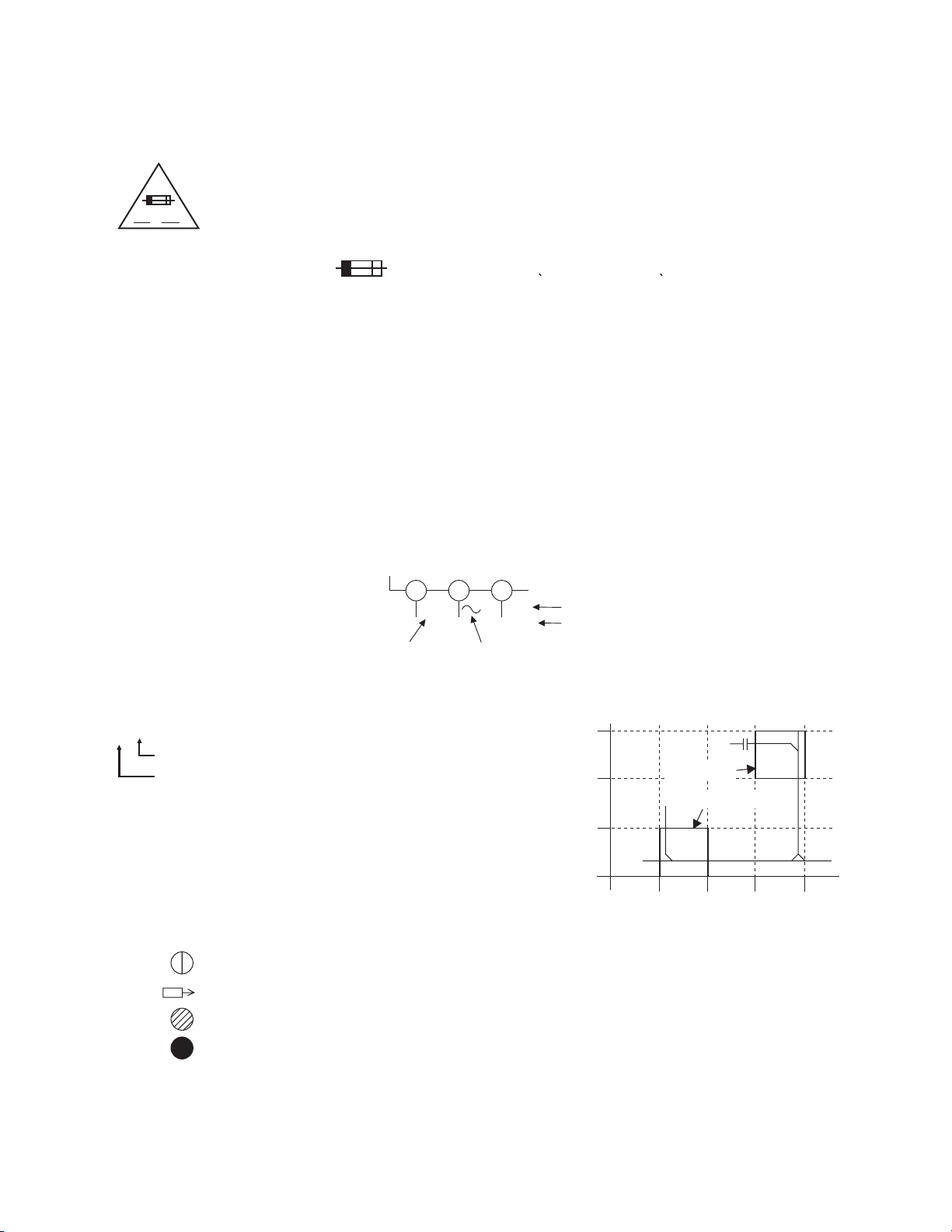
AV 1/3 Schematic Diagram
CAUTION !
Fixed voltage (or Auto voltage selectable) power supply circuit is used in this unit.
If Main Fuse (F1001) is blown , check to see that all components in the power supply
circuit are not defective before you connect the AC plug to the AC power supply.
Otherwise it may cause some components in the power supply circuit to fail.
F
A V
CAUTION !
For continued protection against fire hazard,
replace only with the same type fuse.
ATTENTION : Pour une protection continue les risqes
d'Incele n'utiliser que des fusible de même type.
Risk of fire-replace fuse as marked.
"This symbol means fast operating fuse."
"Ce symbole reprèsente un fusible à fusion rapide."
NOTE:
The voltage for parts in hot circuit is measured using
hot GND as a common terminal.
1-9-3
E5K55SCAV1
Page 27

AV 2/3 Schematic Diagram
1-9-4
E5K55SCAV2
Page 28

AV 3/3 Schematic Diagram
1-9-5
E5K55SCAV3
Page 29

Front & Power SW Schematic Diagram
1-9-6
E5K55SCF
Page 30
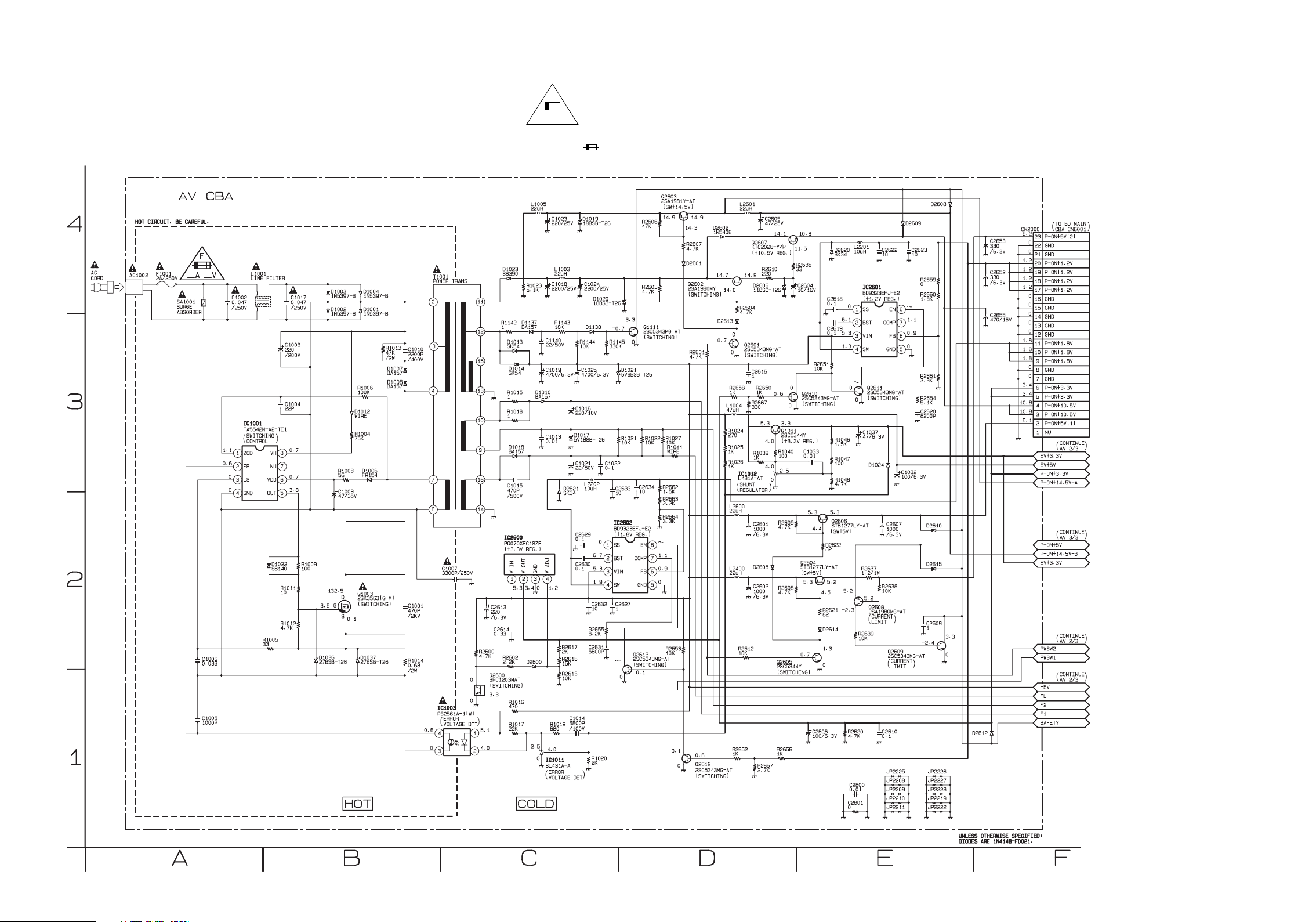
RS232C Schematic Diagram
1-9-7
E5K55SCRS
Page 31
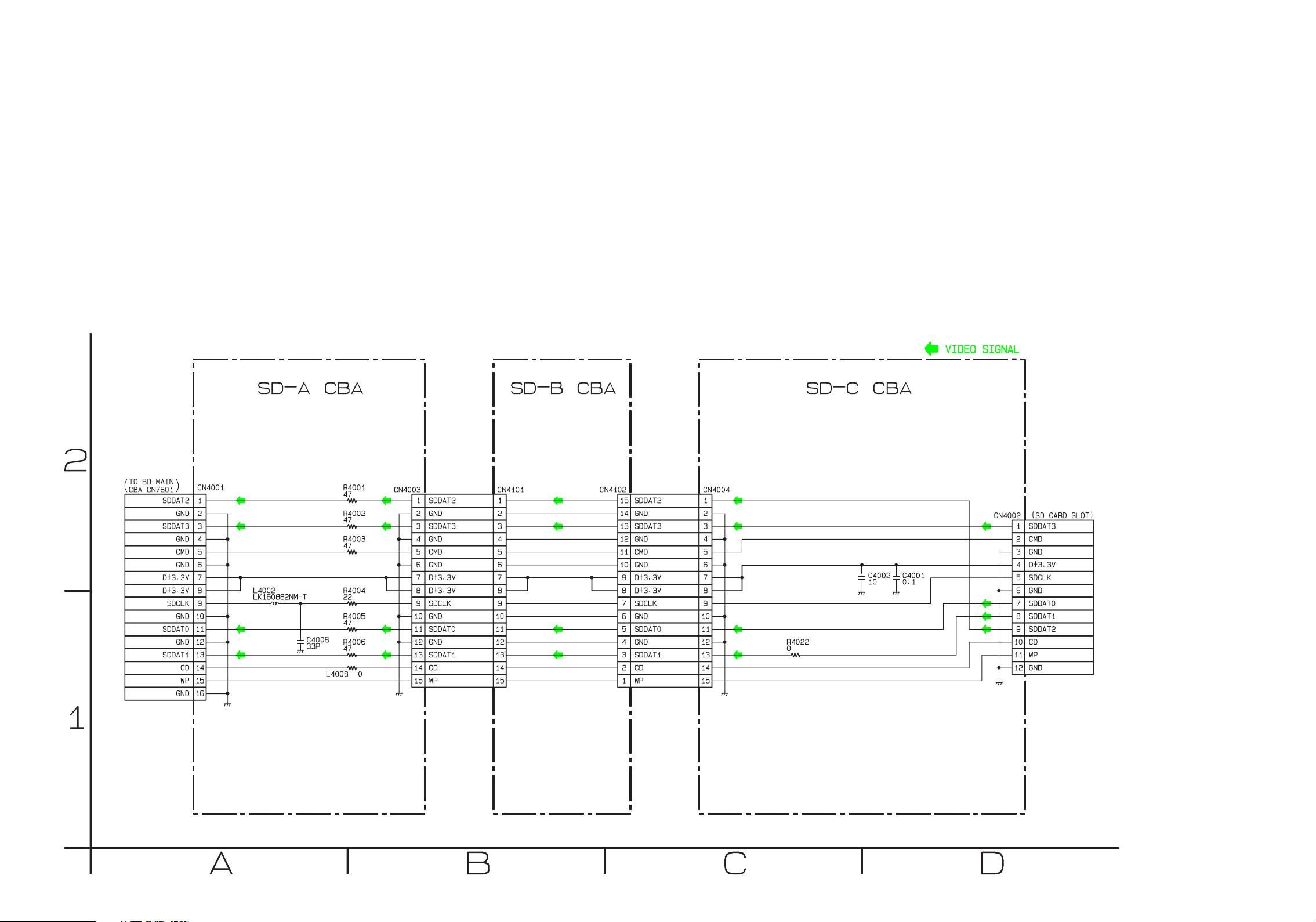
SD-A, SD-B & SD-C Schematic Diagram
1-9-8
E5K55SCSD
Page 32

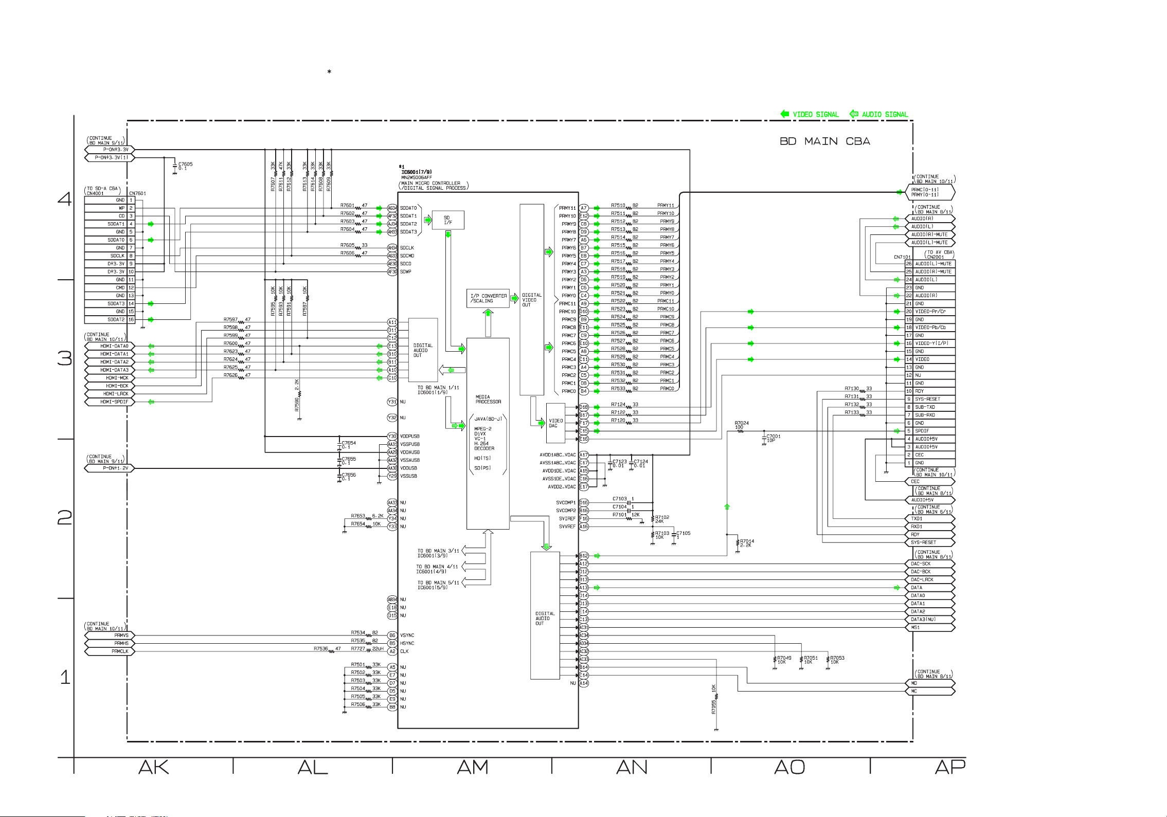
BD Main 1/11 Schematic Diagram
1 NOTE:
The order of pins shown in this diagram is different from that of actual IC6001.
IC6001 is divided into nine and shown as IC6001 (1/9) ~ IC6001 (9/9) in this BD Main Schematic Diagram Section.
1-9-9
E5K55SCBD1
Page 33

BD Main 2/11 Schematic Diagram
1 NOTE:
The order of pins shown in this diagram is different from that of actual IC6001.
IC6001 is divided into nine and shown as IC6001 (1/9) ~ IC6001 (9/9) in this BD Main Schematic Diagram Section.
1-9-10
E5K55SCBD2
Page 34

BD Main 3/11 Schematic Diagram
1 NOTE:
The order of pins shown in this diagram is different from that of actual IC6001.
IC6001 is divided into nine and shown as IC6001 (1/9) ~ IC6001 (9/9) in this BD Main Schematic Diagram Section.
1-9-11
E5K55SCBD3
Page 35

BD Main 4/11 Schematic Diagram
1 NOTE:
The order of pins shown in this diagram is different from that of actual IC6001.
IC6001 is divided into nine and shown as IC6001 (1/9) ~ IC6001 (9/9) in this BD Main Schematic Diagram Section.
1-9-12
E5K55SCBD4
Page 36

BD Main 5/11 Schematic Diagram
1 NOTE:
The order of pins shown in this diagram is different from that of actual IC6001.
IC6001 is divided into nine and shown as IC6001 (1/9) ~ IC6001 (9/9) in this BD Main Schematic Diagram Section.
1-9-13
E5K55SCBD5
Page 37

BD Main 6/11 Schematic Diagram
1 NOTE:
The order of pins shown in this diagram is different from that of actual IC6001.
IC6001 is divided into nine and shown as IC6001 (1/9) ~ IC6001 (9/9) in this BD Main Schematic Diagram Section.
1-9-14
E5K55SCBD6
Page 38
BD Main 7/11 Schematic Diagram
1 NOTE:
The order of pins shown in this diagram is different from that of actual IC6001.
IC6001 is divided into nine and shown as IC6001 (1/9) ~ IC6001 (9/9) in this BD Main Schematic Diagram Section.
1-9-15
E5K55SCBD7
Page 39

BD Main 8/11 Schematic Diagram
1-9-16
E5K55SCBD8
Page 40

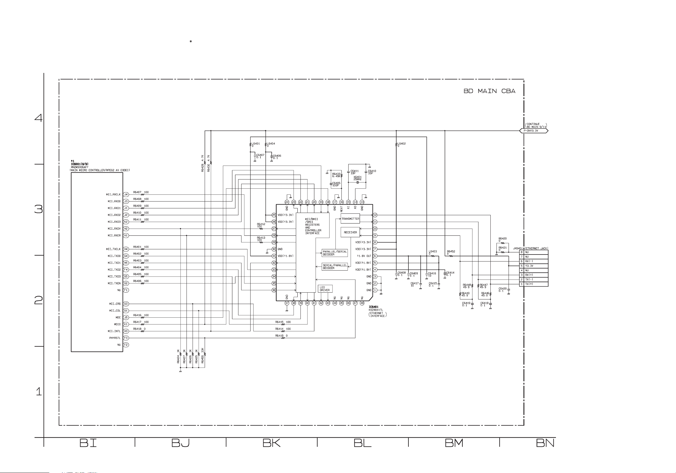
BD Main 9/11 Schematic Diagram
1 NOTE:
The order of pins shown in this diagram is different from that of actual IC6001.
IC6001 is divided into nine and shown as IC6001 (1/9) ~ IC6001 (9/9) in this BD Main Schematic Diagram Section.
1-9-17
E5K55SCBD9
Page 41

BD Main 10/11 Schematic Diagram
1-9-18
E5K55SCBD10
Page 42
BD Main 11/11 Schematic Diagram
1 NOTE:
The order of pins shown in this diagram is different from that of actual IC6001.
IC6001 is divided into nine and shown as IC6001 (1/9) ~ IC6001 (9/9) in this BD Main Schematic Diagram Section.
1-9-19
E5K55SCBD11
Page 43

AV CBA Top View
"Ce symbole reprèsente un fusible à fusion rapide."
CAUTION !
For continued protection against fire hazard,
replace only with the same type fuse.
ATTENTION : Pour une protection continue les risqes
d'Incele n'utiliser que des fusible de même type.
Risk of fire-replace fuse as marked.
"This symbol means fast operating fuse."
A V
F
Because a hot chassis ground is present in the power
supply circut, an isolation transformer must be used.
Also, in order to have the ability to increase the input
slowly, when troubleshooting this type power supply
circuit, a variable isolation transformer is required.
CAUTION !
Fixed voltage (or Auto voltage selectable) power supply circuit is used in this unit.
If Main Fuse (F1001) is blown , check to see that all components in the power supply
circuit are not defective before you connect the AC plug to the AC power supply.
Otherwise it may cause some components in the power supply circuit to fail.
NOTE:
The voltage for parts in hot circuit is measured using
hot GND as a common terminal.
1-9-20
BE5K20F01012A
Page 44

AV CBA Bottom View
"Ce symbole reprèsente un fusible à fusion rapide."
CAUTION !
For continued protection against fire hazard,
replace only with the same type fuse.
ATTENTION : Pour une protection continue les risqes
d'Incele n'utiliser que des fusible de même type.
Risk of fire-replace fuse as marked.
"This symbol means fast operating fuse."
A V
F
Because a hot chassis ground is present in the power
supply circut, an isolation transformer must be used.
Also, in order to have the ability to increase the input
slowly, when troubleshooting this type power supply
circuit, a variable isolation transformer is required.
NOTE:
The voltage for parts in hot circuit is measured using
hot GND as a common terminal.
CAUTION !
Fixed voltage (or Auto voltage selectable) power supply circuit is used in this unit.
If Main Fuse (F1001) is blown , check to see that all components in the power supply
circuit are not defective before you connect the AC plug to the AC power supply.
Otherwise it may cause some components in the power supply circuit to fail.
1-9-21
BE5K20F01012A
Page 45

Front CBA Top View
Power SW CBA Top View
Front CBA Bottom View
Power SW CBA Bottom View
1-9-22
BE5K50F01031A
BE5K50F01031B
Page 46
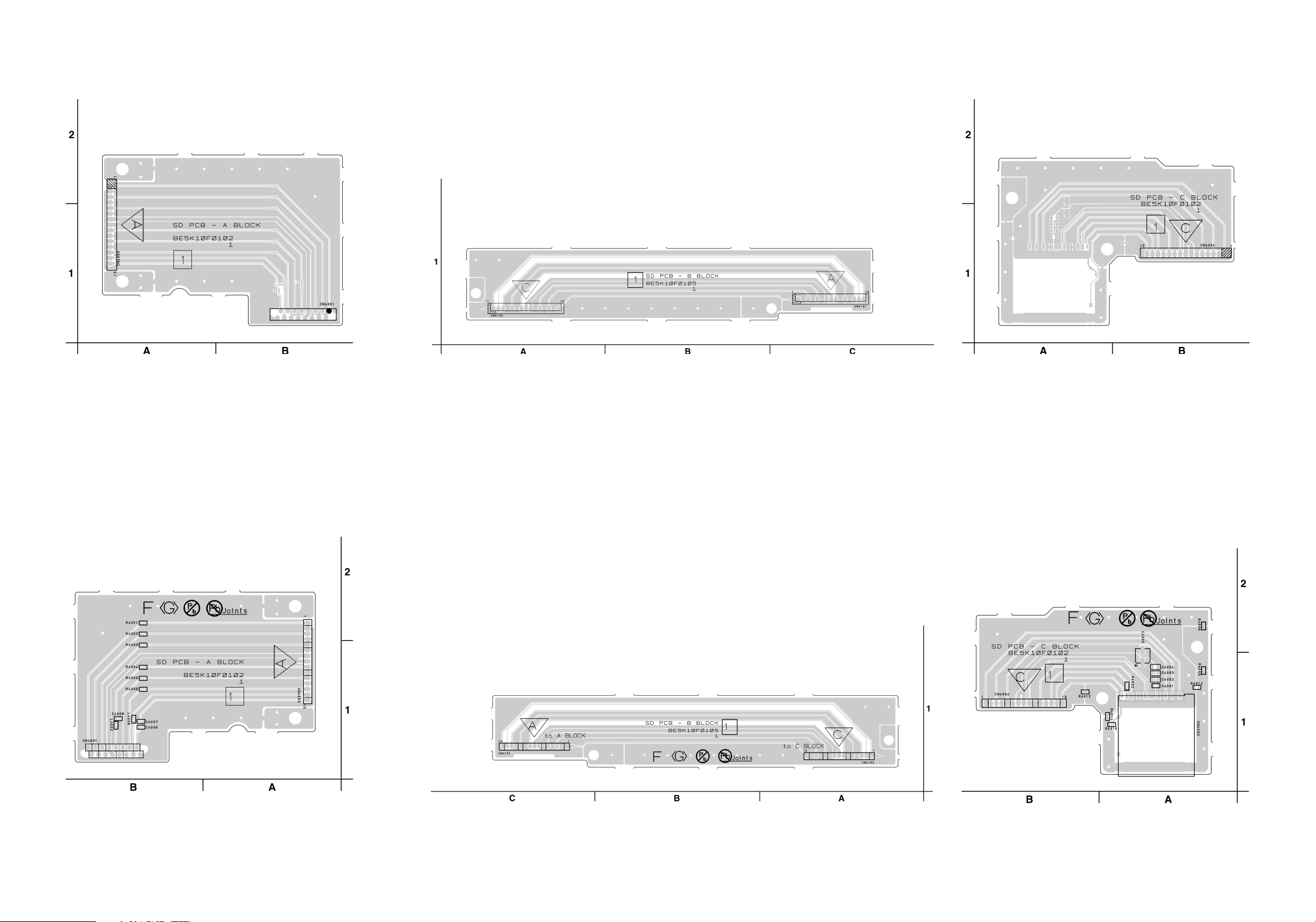
SD-A CBA Top View
SD-B CBA Top View
SD-C CBA Top View
SD-A CBA Bottom View
SD-B CBA Bottom View
SD-C CBA Bottom View
BE5K10F01021A
1-9-23
BE5K10F01051
BE5K10F01021C
Page 47
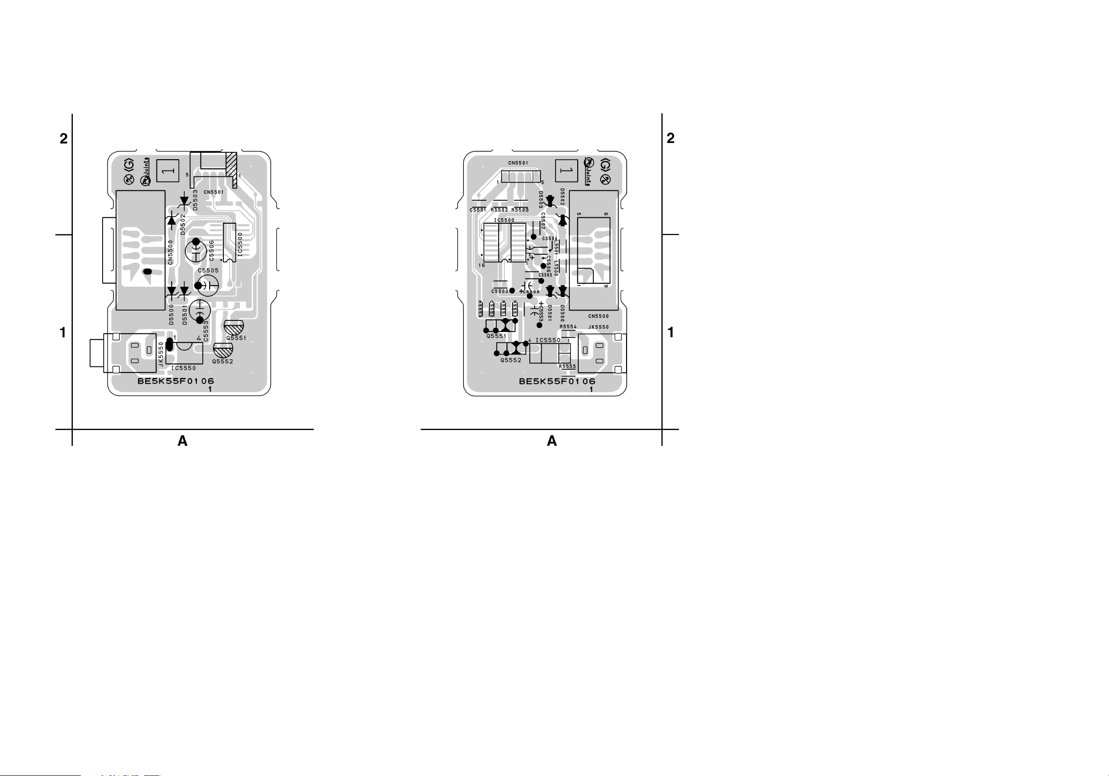
RS232C CBA Top View
RS232C CBA Bottom View
1-9-24
BE5K55F01061
Page 48

Cabinet
EXPLODED VIEWS
See Electrical Parts List
for parts with this mark.
Some Ref. Numbers are
not in sequence.
BD Main CBA &
BD Mechanism Assembly
2L085
2L082
2L049
B32
A3
RS232C CBA
2L034
B70
WX5500
2L081
2L084
2L083
2L061
2L084
2L082
2L082
2L081
2L070
2L071
1B1
Power SW CBA
2L024
A1X
A6
B68
AV CBA
B15
B69
SD-A CBA
SD-B CBA
2L024
2L086
A6
2L051
B70
2L055
2L051
2L024
B47
B13
SD-C CBA
F1001
A6
B5
B4
2L072
FM1001
A4
2L026
2L038
A2
A6
A22
Front CBA
1-10-1 E5K55CEX
Page 49

Packing
Lower Side Upper Side
Some Ref. Numbers
are not in sequence.
S1
S3
X14 X15X6
X19
X10
X2-AX40
X1-A
A21
S1
A21
S2
1-10-2 E5K55PEX
Page 50

MECHANICAL PARTS LIST
PRODUCT SAFETY NOTE: Products marked with a
# have special characteristics important to safety.
Before replacing any of these components, read
carefully the product safety notice in this service
manual. Don't degrade the safety of the product
through improper servicing.
NOTE: Parts that are not assigned part numbers
(---------) are not available.
Ref. No. Description Part No.
A1X FRONT ASSEMBLY E5K55UD 1VM123180
A2 CHASSIS E5K50UD 1VM330278
A3 TOP COVER E5K20UD 1VM122080
A4 REAR PANEL E5K55UD 1VM227377
A6 FOOT ASSEMBLY E5H50UD 1VM430199A
A21 BAR CODE LABEL E5K55UD ----------
A22 LICENSE LABEL E5K12UD ----------
2L024 SCREW P-TIGHT M3X8 BIND HEAD+ GBJP3080
2L026 SCREW C-TIGHT M3X6 E5610UD 0VM412937A
2L034 SCREW C-TIGHT M3X6 E5610UD 0VM412937A
2L038 SCREW C-TIGHT M3X6 E5610UD 0VM412937A
2L049 SCREW C-TIGHT M3X6 E5610UD 0VM412937A
2L051 SCREW C-TIGHT M3X6 E5610UD 0VM412937A
2L061 HEXAGON SPACER E6AE0UD 1VM424730
2L070 B-TIGHT SCREW M3X8 E5E00UD 1VM428563
2L071 B-TIGHT SCREW M3X8 E5E00UD 1VM428563
2L072 SCREW TAP TIGHT M3X8 BIND PAN
2L081 S-TIGHT SCREW M3X6 E5E00UD 1VM428564
2L082 SCREW TAP TIGHT M3X5 BIND HEAD+BLK NI GBHC3050
2L083 S-TIGHT SCREW M3X6 E5E00UD 1VM428564
2L084 S-TIGHT SCREW M3X6 E5E00UD 1VM428564
2L085 SCREW S-TIGHT M3X10 E5610UD 0VM412936A
2L086 SCREW S-TIGHT M3X5 E5K10UD 1VM431079
B4 POWER HOLDER E5K20UD 1VM225697
B5 FAN HOLDER E6700UD 1VM320504L
B13 SD PCB BRACKET E5K10UD 1VM329203
B15 SHIELD BRACKET E5K10UD 1VM226756
B32 MAIN PCB EARTH PLATE E5K20UD 1VM430800
B68 FRONT SHIELD E5K20UD 1VM328838
B69 PORON SPONGE E5K20UD 1VM431100
B70 TAPE HIMERON(60*6) HG470ED 1VM421170
FM1001 MOTOR DC FAN 2D57NL100010 MMEZR12XNR05
WX5500 WIRE ASSEMBLY AV-RS232C 5PIN WIRE
HEAD+BLK NI
WX1E5K55-001
PAC K IN G
S1 SIDE PAD E5K50UD 1VM123159
S2 GIFT BOX CARTON E5K55UD 1VM330521
S3 SET BAG E7708UA 0DM400731D
ACCESSORIES
X1-A# OWNERS MANUAL E5K55UD 1VMN27613
X2-A QUICK GUIDE E5K55UD 1VMN27614
X6 MANGANESE DRY BATTERY R6UWC/2STA XB0M311MS003
X10 ACCESSORY BAG E5795ED 0VM416059
X14 AV CORD 1000/BLACK WPZ0102TM018
X15# AC CORD WITH A GND WIRE UL/CSA/ 162/
X19 REMOTE CONTROL UNIT NB822UD NB822UD
X40 WARRANTY CARD E5H55UD 1VMN26326
NO/BLACK
GPHB3080
WX1E5K55-001
WAV0162LW001
20090604 1-11-1 E5K55CA
Page 51
ELECTRICAL PARTS LIST
PRODUCT SAFETY NOTE: Products marked with a
# have special characteristics important to safety.
Before replacing any of these components, read
carefully the product safety notice in this service
manual. Don't degrade the safety of the product
through improper servicing.
NOTES:
1. Parts that are not assigned part numbers (---------)
are not available.
2. Tolerance of Capacitors and Resistors are noted
with the following symbols.
C.....±0.25% D.....±0.5% F.....±1%
G.....±2% J......±5% K.....±10%
M.....±20% N.....±30% Z.....+80/-20%
BD MAIN CBA & BD MECHANISM
ASSEMBLY
Ref. No. Description Part No.
1B1 BD MAIN CBA & BD MECHANISM ASSEMBLY N77R1BUN
AV CBA
Ref. No. Description Part No.
AV C BA
Consists of the following:
CAPACITORS
C1001 CAP CERAMIC 470pF/2KV/K CA3D471PAN17
C1002# LINE ACROSS CAP. 0.047µF/250V K CT2E473DC016
C1004 CHIP CERAMIC CAP.(1608) CH J 22pF/50V CHD1JJ3CH220
C1005 CHIP CERAMIC CAP.(1608) B K 1000pF/50V CHD1JK30B102
C1006 CHIP CERAMIC CAP.(1608) B K 0.033µF/50V CHD1JK30B333
C1007# SAFETY CAP. 3300pF/250V CCD2EMA0E332
C1008 ELECTROLYTIC CAPACITOR
C1009 ELECTROLYTIC CAP. 47µF/35V/M CEE47RENW016
C1010 METALIZED FILM CAP. 0.0022µF/400V K CT2H222DT034
C1013 CHIP CERAMIC CAP.(1608) B K 0.01µF/50V CHD1JK30B103
C1014 POLYESTER FILM CAP. (PB FREE) 0.0068µF/
C1015 CERAMIC CAP. B K 470pF/500V CCD2JKS0B471
C1016 ELECTROLYTIC CAP. 220µF/10V M CEB221ENW016
C1017# LINE ACROSS CAP. 0.047µF/250V K CT2E473DC016
C1018 ELECTROLYTIC CAP 2200µF/25V/M CED222ENW009
C1019 ELECTROLYTIC CAP 4700µF/6.3V/M CEA472ENW009
C1021 ELECTROLYTIC CAP. 22µF/50V/M CEF22RENW016
C1022 CHIP CERAMIC CAP.(1608) F Z 0.1µF/50V CHD1JZ30F104
C1023 ELECTROLYTIC CAP. 220µF/25V/M CED221ENW016
C1024 ELECTROLYTIC CAP 2200µF/25V/M CED222ENW009
C1025 ELECTROLYTIC CAP 4700µF/6.3V/M CEA472ENW009
C1032 ELECTROLYTIC CAP. 100µF/6.3V/M CEA101ENW016
C1033 CHIP CERAMIC CAP.(1608) B K 0.01µF/50V CHD1JK30B103
C1037 ELECTROLYTIC CAP. 47µF/6.3V/M CEA47RENW016
C1140 ELECTROLYTIC CAP. 22µF/50V/M CEF22RENW016
C2000 CHIP CERAMIC CAP.(1608) B K 0.1µF/25V CHD1EK30B104
C2001 ELECTROLYTIC CAP. 100µF/16V/M CEC101ENW016
C2002 CHIP CERAMIC CAP.(1608) B K 0.1µF/25V CHD1EK30B104
C2005 CHIP CERAMIC CAP.(1608) F Z 0.1µF/50V CHD1JZ30F104
ZR200TA221K18EB
100V J
1VSA22029
CA2D221DYG04
CA2A682DT018
Ref. No. Description Part No.
C2007 CHIP CERAMIC CAP.(1608) F Z 0.1µF/50V CHD1JZ30F104
C2009 CHIP CERAMIC CAP.(1608) CH J 100pF/50V CHD1JJ3CH101
C2011 CHIP CERAMIC CAP.(1608) F Z 0.1µF/50V CHD1JZ30F104
C2013 CHIP CERAMIC CAP.(1608) B K 0.015µF/50V CHD1JK30B153
C2016 ELECTROLYTIC CAP. 47µF/6.3V/M CEA47RENW016
C2065 CHIP CERAMIC CAP.(1608) B K 1000pF/50V CHD1JK30B102
C2100 CHIP CERAMIC CAP.(1608) B K 0.1µF/25V CHD1EK30B104
C2104 ELECTROLYTIC CAP. 47µF/6.3V/M CEA47RENW016
C2106 CHIP CERAMIC CAP. CH D 8pF/50V CHD1JD3CH8R0
C2108 CHIP CERAMIC CAP.(1608) F Z 0.1µF/50V CHD1JZ30F104
C2180 CHIP CERAMIC CAP.(1608) F Z 0.1µF/50V CHD1JZ30F104
C2181 ELECTROLYTIC CAP. 220µF/6.3V/M CEA221ENW016
C2204 ELECTROLYTIC CAP. 47µF/25V/M CED47RENW016
C2205 ELECTROLYTIC CAP. 470µF/6.3V/M CEA471ENW016
C2206 CHIP CERAMIC CAP.(1608) F Z 0.1µF/50V CHD1JZ30F104
C2207 ELECTROLYTIC CAP. 10µF/16V/M CEC10RENW016
C2208 ELECTROLYTIC CAP. 10µF/16V/M CEC10RENW016
C2209 CHIP CERAMIC CAP. CH J 220pF/50V CHD1JJ3CH221
C2210 CHIP CERAMIC CAP. CH J 220pF/50V CHD1JJ3CH221
C2211 ELECTROLYTIC CAP. 10µF/16V/M CEC10RENW016
C2212 ELECTROLYTIC CAP. 10µF/16V/M CEC10RENW016
C2213 CHIP CERAMIC CAP.(1608) F Z 0.1µF/50V CHD1JZ30F104
C2215 CHIP CERAMIC CAP. CH J 39pF/50V CHD1JJ3CH390
C2216 CHIP CERAMIC CAP. CH J 39pF/50V CHD1JJ3CH390
C2280 CHIP CERAMIC CAP.(1608) F Z 0.1µF/50V CHD1JZ30F104
C2281 ELECTROLYTIC CAP. 220µF/6.3V/M CEA221ENW016
C2283 ELECTROLYTIC CAP. 1000µF/6.3V/M CEA102ENW016
C2284 CHIP CERAMIC CAP.(1608) F Z 0.1µF/50V CHD1JZ30F104
C2286 CHIP CERAMIC CAP.(1608) F Z 0.1µF/50V CHD1JZ30F104
C2300 ELECTROLYTIC CAP. 100µF/6.3V/M CEA101ENW016
C2301 CHIP CERAMIC CAP.(1608) F Z 0.1µF/50V CHD1JZ30F104
C2314 CHIP CERAMIC CAP.(1608) F Z 0.1µF/50V CHD1JZ30F104
C2315 CHIP CERAMIC CAP.(1608) F Z 0.1µF/50V CHD1JZ30F104
C2316 ELECTROLYTIC CAP. 22µF/6.3V/M CEA22RENW016
C2319 CHIP CERAMIC CAP.(1608) B K 0.1µF/50V CHD1JK30B104
C2320 CHIP CERAMIC CAP.(1608) B K 1µF/10V CHD1AK30B105
C2321 CHIP CERAMIC CAP.(1608) B K 1µF/10V CHD1AK30B105
C2322 ELECTROLYTIC CAP. 33µF/10V/M CEB33RENW016
C2323 ELECTROLYTIC CAP. 330µF/6.3V/M CEA331ENW016
C2324 ELECTROLYTIC CAP. 330µF/6.3V/M CEA331ENW016
C2325 ELECTROLYTIC CAP. 33µF/10V/M CEB33RENW016
C2326 ELECTROLYTIC CAP. 330µF/6.3V/M CEA331ENW016
C2327 ELECTROLYTIC CAP. 330µF/6.3V/M CEA331ENW016
C2328 CHIP CERAMIC CAP.(1608) B K 0.1µF/50V CHD1JK30B104
C2329 ELECTROLYTIC CAP. 100µF/6.3V/M CEA101ENW016
C2330 ELECTROLYTIC CAP. 100µF/6.3V/M CEA101ENW016
C2601 ELECTROLYTIC CAP. 1000µF/6.3V/M CEA102ENW016
C2602 ELECTROLYTIC CAP. 1000µF/6.3V/M CEA102ENW016
C2604 ELECTROLYTIC CAP. 10µF/16V/M CEC10RENW016
C2605 ELECTROLYTIC CAP. 47µF/25V/M CED47RENW016
C2606 ELECTROLYTIC CAP. 100µF/6.3V/M CEA101ENW016
C2607 ELECTROLYTIC CAP. 1000µF/6.3V/M CEA102ENW016
C2609 CHIP CERAMIC CAP.(1608) B K 1µF/10V CHD1AK30B105
C2610 CHIP CERAMIC CAP.(1608) B K 0.1µF/25V CHD1EK30B104
C2613 ELECTROLYTIC CAP. 220µF/6.3V/M CEA221ENW016
C2614 CHIP CERAMIC CAP.(1608) B K 0.33µF/10V CHD1AK30B334
C2616 CHIP CERAMIC CAP.(1608) B K 1µF/10V CHD1AK30B105
C2618 CHIP CERAMIC CAP.(1608) F Z 0.1µF/50V CHD1JZ30F104
C2619 CHIP CERAMIC CAP.(1608) F Z 0.1µF/50V CHD1JZ30F104
C2620 CHIP CERAMIC CAP. B K 8200pF/50V CHD1JK30B822
20090604 1-12-1 E5K55EL
Page 52

Ref. No. Description Part No.
C2622 CHIP CERAMIC CAP.(2125) B K 10µF/6.3V CHE0KK30B106
C2623 CHIP CERAMIC CAP.(2125) B K 10µF/6.3V CHE0KK30B106
C2627 CHIP CERAMIC CAP.(1608) B K 1µF/10V CHD1AK30B105
C2629 CHIP CERAMIC CAP.(1608) F Z 0.1µF/50V CHD1JZ30F104
C2630 CHIP CERAMIC CAP.(1608) F Z 0.1µF/50V CHD1JZ30F104
C2631 CHIP CERAMIC CAP.(1608) B K 5600pF/50V CHD1JK30B562
C2632 CHIP CERAMIC CAP.(2125) B K 10µF/6.3V CHE0KK30B106
C2633 CHIP CERAMIC CAP.(2125) B K 10µF/6.3V CHE0KK30B106
C2634 CHIP CERAMIC CAP.(2125) B K 10µF/6.3V CHE0KK30B106
C2638 CHIP CERAMIC CAP. CH J 330pF/50V CHD1JJ3CH331
C2639 CHIP CERAMIC CAP. CH J 220pF/50V CHD1JJ3CH221
C2640 CHIP CERAMIC CAP.(1608) B K 0.01µF/50V CHD1JK30B103
C2652 ELECTROLYTIC CAP. 330µF/6.3V/M CEA331ENW016
C2653 ELECTROLYTIC CAP. 330µF/6.3V/M CEA331ENW016
C2655 ELECTROLYTIC CAP. 470µF/16V/M CEC471ENW016
C2800 CHIP CERAMIC CAP.(1608) B K 0.01µF/50V CHD1JK30B103
C2801 CHIP RES.(1608) 1/10W 0 Ω RRXAZR5Z0000
CONNECTORS
CN2000 TWG CONNECTOR 23P TWG-P23P-A1 J3TWA23TG001
CN2001 WIRE ASSEMBLY AV-MAIN 26P WX1E5K20-
CN2002 FFC CONNECTOR IMSA-9615S-16A-PP-A JC96J16ER007
CN2004 PH CONNECTOR TOP 2P B2B-PH-K-S
CN2006 CONNECTOR PRINT OSU B5B-PH-K-S
001
(LF)(SN)
(LF)(SN)
WX1E5K20-001
J3PHC02JG029
J3PHC05JG029
DIODES
D1001 DIODE 1N5397-B NDLZ001N5397
D1002 DIODE 1N5397-B NDLZ001N5397
D1003 DIODE 1N5397-B NDLZ001N5397
D1004 DIODE 1N5397-B NDLZ001N5397
D1006 DIODE FR154 NDLZ000FR154
D1007 RECTIFIER DIODE BA157 NDQZ000BA157
D1008 RECTIFIER DIODE BA157 NDQZ000BA157
D1010 RECTIFIER DIODE BA157 NDQZ000BA157
D1012 PCB JUMPER D0.6-P15.0 JW15.0T
D1013 SCHOTTKY BARRIER DIODE SMD SK54 ND1Z0000SK54
D1014 SCHOTTKY BARRIER DIODE SMD SK54 ND1Z0000SK54
D1017 DIODE ZENER 5V1BSB-T26 NDTB5R1BST26
D1018 RECTIFIER DIODE BA157 NDQZ000BA157
D1019 DIODE ZENER 18BSB-T26 NDTB018BST26
D1020 DIODE ZENER 18BSB-T26 NDTB018BST26
D1021 DIODE ZENER 6V8BSB-T26 NDTB6R8BST26
D1022 SCHOTTKY BARRIER DIODE SB140 NDQZ000SB140
D1023 SCHOTTKY BARRIER DIODE SMD SK39 ND1Z0000SK39
D1024 DIODE SWITCHING 1N4148-F0021 NDTZ01N4148F
D1036 DIODE ZENER 27BSB-T26 NDTB027BST26
D1037 DIODE ZENER 27BSB-T26 NDTB027BST26
D1137 RECTIFIER DIODE BA157 NDQZ000BA157
D1138 DIODE SWITCHING 1N4148-F0021 NDTZ01N4148F
D2001 DIODE SWITCHING 1N4148-F0021 NDTZ01N4148F
D2002 DIODE SWITCHING 1N4148-F0021 NDTZ01N4148F
D2003 DIODE ZENER 36BSA-T26 NDTA036BST26
D2004 DIODE SWITCHING 1N4148-F0021 NDTZ01N4148F
D2600 DIODE SWITCHING 1N4148-F0021 NDTZ01N4148F
D2601 DIODE SWITCHING 1N4148-F0021 NDTZ01N4148F
D2602 DIODE 1N5406 NDLZ001N5406
D2605 DIODE SWITCHING 1N4148-F0021 NDTZ01N4148F
D2606 DIODE ZENER 11BSC-T26 NDTC011BST26
D2608 DIODE SWITCHING 1N4148-F0021 NDTZ01N4148F
D2609 DIODE SWITCHING 1N4148-F0021 NDTZ01N4148F
D2610 DIODE SWITCHING 1N4148-F0021 NDTZ01N4148F
D2612 DIODE SWITCHING 1N4148-F0021 NDTZ01N4148F
Ref. No. Description Part No.
D2613 DIODE SWITCHING 1N4148-F0021 NDTZ01N4148F
D2614 DIODE SWITCHING 1N4148-F0021 NDTZ01N4148F
D2615 DIODE SWITCHING 1N4148-F0021 NDTZ01N4148F
D2620 SCHOTTKY BARRIER DIODE SMD SK34 ND1Z0000SK34
D2621 SCHOTTKY BARRIER DIODE SMD SK34 ND1Z0000SK34
D2624 DIODE ZENER 4V7BSB-T26 NDTB4R7BST26
ICS
IC1001 IC SWITCHING FA5542N-A2-TE1 SOP8 QSZBA0TFD005
IC1003# PHOTOCOUPLER PS2561A-1(W) QPEWPS2561A1
IC1011 IC SHUNT REGULATOR SL431A-AT NSZBA0TAUK01
IC1012 IC SHUNT REGULATOR SL431A-AT NSZBA0TAUK01
IC2000 IC SUB MICON MN101C77A GC QSAA0R0MS010
IC2001 RESET IC S-80930CNMC-G80T2G QSCA0T0SK018
IC2200 IC OP AMP UTC4580TE NSCA0T02H001
IC2300 IC VIDEO DRIVER MM1757EHBE QSCA0T0MM001
IC2600 IC VOLTAGE REGULATOR PQ070XFC1SZF /
IC2601 IC DC-DC CONVERTER BD9323EFJ-E2 QSCA0T0RM002
IC2602 IC DC-DC CONVERTER BD9323EFJ-E2 QSCA0T0RM002
4PIN
QSZBA0RSH083
COILS
L1001# LINE FILTER 27MH 5703 LLBG00ZKT009
L1003 POWER INDUCTORS CWKBNP-220K LLF2200KV002
L1004 RADIAL TYPE CHOKE COIL CW68-470K-
L1005 CHOKE COIL 22µH-K LLBD00PKV021
L2100 INDUCTOR(0.47µH K) LAP02TAR47K LLAXKATTUR47
L2201 POWER INDUCTORS CWKBNP-100K LLF1000KV002
L2202 POWER INDUCTORS CWKBNP-100K LLF1000KV002
L2300 RADIAL TYPE CHOKE COIL CW68-470K-
L2301 CHIP RES.(1608) 1/10W 0 Ω RRXAZR5Z0000
L2306 PCB JUMPER D0.6-P5.0 JW5.0T
L2400 CHOKE COIL 22µH-K LLBD00PKV021
L2600 CHOKE COIL 22µH-K LLBD00PKV021
L2601 CHOKE COIL 22µH-K LLBD00PKV021
841040NP
841040NP
LLBD00PKV023
LLBD00PKV023
TRANSISTORS
Q1003# FET MOS 2SK3563(Q M) QFQZSK3563QM
Q1011 NPN TRANSISTOR 2SC5344 Y NQSY02SC5344
Q1111 NPN TRANSISTOR 2SC5343MG-AT NQSG2SC5343M
Q2000 PNP TRANSISTOR 2SA1980M Y NQSY2SA1980M
Q2001 NPN TRANSISTOR RES-IN SRC1203MAT NQSZSRC1203M
Q2002 PNP TRANSISTOR 2SA1980M Y NQSY2SA1980M
Q2003 NPN TRANSISTOR RES-IN SRC1203MAT NQSZSRC1203M
Q2012 PNP TRANSISTOR 2SA1980M Y NQSY2SA1980M
Q2013 NPN TRANSISTOR 2SC5343MG-AT NQSG2SC5343M
Q2014 PNP TRANSISTOR 2SA1981Y-AT NQSY02SA1981
Q2100 NPN TRANSISTOR 2SC5343MG-AT NQSG2SC5343M
Q2101 NPN TRANSISTOR 2SC5343MG-AT NQSG2SC5343M
Q2200 PNP TRANSISTOR RES-IN SRA2205M NQSZSRA2205M
Q2201 PNP TRANSISTOR RES-IN SRA2205M NQSZSRA2205M
Q2202 NPN TRANSISTOR 2SC5343MG-AT NQSG2SC5343M
Q2203 NPN TRANSISTOR 2SC5343MG-AT NQSG2SC5343M
Q2204 PNP TRANSISTOR 2SA1980M Y NQSY2SA1980M
Q2205 NPN TRANSISTOR 2SC5343MG-AT NQSG2SC5343M
Q2600 NPN TRANSISTOR RES-IN SRC1203MAT NQSZSRC1203M
Q2601 NPN TRANSISTOR 2SC5343MG-AT NQSG2SC5343M
Q2602 PNP TRANSISTOR 2SA1980M Y NQSY2SA1980M
Q2603 PNP TRANSISTOR 2SA1981Y-AT NQSY02SA1981
Q2604 PNP TRANSISTOR STB1277LY-AT NQSYSTB1277L
Q2605 NPN TRANSISTOR 2SC5344 Y NQSY02SC5344
Q2606 PNP TRANSISTOR STB1277LY-AT NQSYSTB1277L
Q2607 TRANSISTOR(PB FREE) KTC2026-Y/P NQEYKTC2026P
Q2608 PNP TRANSISTOR 2SA1980MG-AT NQSG2SA1980M
20090604 1-12-2 E5K55EL
Page 53

Ref. No. Description Part No.
Q2609 NPN TRANSISTOR 2SC5343MG-AT NQSG2SC5343M
Q2610 NPN TRANSISTOR 2SC5343MG-AT NQSG2SC5343M
Q2611 NPN TRANSISTOR 2SC5343MG-AT NQSG2SC5343M
Q2612 NPN TRANSISTOR 2SC5343MG-AT NQSG2SC5343M
Q2613 NPN TRANSISTOR 2SC5343MG-AT NQSG2SC5343M
Q2614 NPN TRANSISTOR 2SC5343MG-AT NQSG2SC5343M
Q2618 NPN TRANSISTOR 2SC5343MG-AT NQSG2SC5343M
Q2619 NPN TRANSISTOR 2SC5343MG-AT NQSG2SC5343M
Q2620 NPN TRANSISTOR 2SC5343MG-AT NQSG2SC5343M
Q2621 NPN TRANSISTOR 2SC5343MG-AT NQSG2SC5343M
RESISTORS
R1004 CARBON RES. 1/4W J 75k Ω RCX4JATZ0753
R1005 CARBON RES. 1/4W J 33 Ω RCX4JATZ0330
R1006 CARBON RES. 1/4W J 100k Ω RCX4JATZ0104
R1008 CARBON RES. 1/4W J 56 Ω RCX4JATZ0560
R1009 CARBON RES. 1/4W J 100 Ω RCX4JATZ0101
R1011 CARBON RES. 1/4W J 10 Ω RCX4JATZ0100
R1012 CARBON RES. 1/4W J 4.7k Ω RCX4JATZ0472
R1013 METAL OXIDE FILM RES. 2W J 47k Ω RN02473ZU001
R1014 METAL OXIDE FILM RES. 2W J 0.68 Ω RN02R68ZU001
R1015 CHIP RES. 1/10W J 1 Ω RRXAJR5Z01R0
R1016 CHIP RES. 1/10W J 470 Ω RRXAJR5Z0471
R1017 CHIP RES. 1/10W J 22k Ω RRXAJR5Z0223
R1018 CHIP RES. 1/10W J 1 Ω RRXAJR5Z01R0
R1019 CHIP RES. 1/10W J 680 Ω RRXAJR5Z0681
R1020 CHIP RES. 1/10W F 2k Ω RRXAFR5H2001
R1021 CARBON RES. 1/4W J 10k Ω RCX4JATZ0103
R1022 CARBON RES. 1/4W J 10k Ω RCX4JATZ0103
R1023 CARBON RES. 1/4W J 5.1k Ω RCX4JATZ0512
R1024 CHIP RES. 1/10W F 270 Ω RRXAFR5H2700
R1025 CHIP RES. 1/10W F 1.0k Ω RRXAFR5H1001
R1026 CHIP RES. 1/10W F 1.0k Ω RRXAFR5H1001
R1027 CARBON RES. 1/4W J 10k Ω RCX4JATZ0103
R1039 CHIP RES. 1/10W J 1k Ω RRXAJR5Z0102
R1040 CARBON RES. 1/4W J 100 Ω RCX4JATZ0101
R1041 PCB JUMPER D0.6-P5.0 JW5.0T
R1046 CHIP RES. 1/10W F 1.5k Ω RRXAFR5H1501
R1047 CHIP RES. 1/10W F 100 Ω RRXAFR5H1000
R1048 CHIP RES. 1/10W F 4.7k Ω RRXAFR5H4701
R1142 CHIP RES. 1/10W J 1 Ω RRXAJR5Z01R0
R1143 CHIP RES. 1/10W F 18k Ω RRXAFR5H1802
R1144 CHIP RES. 1/10W F 10k Ω RRXAFR5H1002
R1145 CHIP RES. 1/10W J 330k Ω RRXAJR5Z0334
R2000 CHIP RES. 1/10W J 1k Ω RRXAJR5Z0102
R2001 CHIP RES. 1/10W J 100 Ω RRXAJR5Z0101
R2002 CHIP RES. 1/10W J 100 Ω RRXAJR5Z0101
R2004 CHIP RES. 1/10W J 470 Ω RRXAJR5Z0471
R2005 CHIP RES.(1608) 1/10W 0 Ω RRXAZR5Z0000
R2006 CHIP RES. 1/10W J 100 Ω RRXAJR5Z0101
R2007 CHIP RES. 1/10W J 100 Ω RRXAJR5Z0101
R2008 CHIP RES. 1/10W J 47k Ω RRXAJR5Z0473
R2018 CHIP RES. 1/10W J 39k Ω RRXAJR5Z0393
R2019 CHIP RES. 1/10W J 22k Ω RRXAJR5Z0223
R2020 CHIP RES. 1/10W J 100 Ω RRXAJR5Z0101
R2024 CHIP RES. 1/10W J 10k Ω RRXAJR5Z0103
R2025 CHIP RES. 1/10W J 10k Ω RRXAJR5Z0103
R2028 CHIP RES. 1/10W J 10k Ω RRXAJR5Z0103
R2029 CHIP RES. 1/10W J 10k Ω RRXAJR5Z0103
R2031 CHIP RES. 1/10W J 100 Ω RRXAJR5Z0101
R2032 CHIP RES. 1/10W J 100 Ω RRXAJR5Z0101
R2033 CHIP RES. 1/10W J 100 Ω RRXAJR5Z0101
R2034 CHIP RES.(1608) 1/10W 0 Ω RRXAZR5Z0000
Ref. No. Description Part No.
R2035 CHIP RES. 1/10W J 10k Ω RRXAJR5Z0103
R2039 CHIP RES. 1/10W J 680 Ω RRXAJR5Z0681
R2050 CHIP RES. 1/10W J 10k Ω RRXAJR5Z0103
R2051 CHIP RES. 1/10W J 1k Ω RRXAJR5Z0102
R2053 CHIP RES. 1/10W J 47k Ω RRXAJR5Z0473
R2056 CHIP RES. 1/10W J 10k Ω RRXAJR5Z0103
R2058 CHIP RES. 1/10W J 10k Ω RRXAJR5Z0103
R2060 CHIP RES. 1/10W J 47k Ω RRXAJR5Z0473
R2061 CHIP RES. 1/10W J 5.6k Ω RRXAJR5Z0562
R2063 CARBON RES. 1/4W J 620 Ω RCX4JATZ0621
R2064 CARBON RES. 1/4W J 620 Ω RCX4JATZ0621
R2065 CARBON RES. 1/4W J 10 Ω RCX4JATZ0100
R2066 CHIP RES. 1/10W J 47k Ω RRXAJR5Z0473
R2067 CHIP RES. 1/10W J 5.6k Ω RRXAJR5Z0562
R2069 CARBON RES. 1/4W J 120 Ω RCX4JATZ0121
R2070 CARBON RES. 1/4W J 120 Ω RCX4JATZ0121
R2073 CARBON RES. 1/4W J 620 Ω RCX4JATZ0621
R2074 CARBON RES. 1/4W J 620 Ω RCX4JATZ0621
R2091 CARBON RES. 1/4W J 47k Ω RCX4JATZ0473
R2092 CARBON RES. 1/4W J 47k Ω RCX4JATZ0473
R2093 CHIP RES. 1/10W J 10k Ω RRXAJR5Z0103
R2094 CHIP RES. 1/10W J 47k Ω RRXAJR5Z0473
R2095 CHIP RES. 1/10W J 3.9k Ω RRXAJR5Z0392
R2100 CHIP RES. 1/10W J 2k Ω RRXAJR5Z0202
R2101 CHIP RES. 1/10W J 2.2k Ω RRXAJR5Z0222
R2102 CHIP RES. 1/10W J 2.2k Ω RRXAJR5Z0222
R2103 CHIP RES. 1/10W J 220 Ω RRXAJR5Z0221
R2104 CHIP RES. 1/10W J 75 Ω RRXAJR5Z0750
R2105 CHIP RES. 1/10W J 100k Ω RRXAJR5Z0104
R2109 CHIP RES.(1608) 1/10W 0 Ω RRXAZR5Z0000
R2115 CARBON RES. 1/4W J 5.6 Ω RCX4JATZ05R6
R2116 CARBON RES. 1/4W J 5.6 Ω RCX4JATZ05R6
R2117 CHIP RES. 1/10W J 1k Ω RRXAJR5Z0102
R2118 CARBON RES. 1/4W J 10 Ω RCX4JATZ0100
R2208 CHIP RES. 1/10W F 24k Ω RRXAFR5H2402
R2209 CHIP RES. 1/10W F 24k Ω RRXAFR5H2402
R2210 CHIP RES. 1/10W J 8.2k Ω RRXAJR5Z0822
R2211 CHIP RES. 1/10W J 8.2k Ω RRXAJR5Z0822
R2212 CHIP RES. 1/10W F 33.0k Ω RRXAFR5H3302
R2213 CHIP RES. 1/10W F 33.0k Ω RRXAFR5H3302
R2214 CHIP RES. 1/10W J 100k Ω RRXAJR5Z0104
R2215 CHIP RES. 1/10W J 100k Ω RRXAJR5Z0104
R2216 CHIP RES. 1/10W J 820 Ω RRXAJR5Z0821
R2217 CHIP RES. 1/10W J 1k Ω RRXAJR5Z0102
R2218 CHIP RES. 1/10W J 820 Ω RRXAJR5Z0821
R2219 CHIP RES. 1/10W J 1k Ω RRXAJR5Z0102
R2220 CHIP RES. 1/10W J 100k Ω RRXAJR5Z0104
R2221 CHIP RES. 1/10W J 100k Ω RRXAJR5Z0104
R2223 CHIP RES. 1/10W J 4.7k Ω RRXAJR5Z0472
R2224 CHIP RES. 1/10W J 2.2k Ω RRXAJR5Z0222
R2226 CHIP RES. 1/10W J 1k Ω RRXAJR5Z0102
R2227 CHIP RES. 1/10W J 220 Ω RRXAJR5Z0221
R2228 CHIP RES. 1/10W J 220 Ω RRXAJR5Z0221
R2229 CHIP RES. 1/10W J 2.2k Ω RRXAJR5Z0222
R2230 CHIP RES. 1/10W J 4.7k Ω RRXAJR5Z0472
R2284 CHIP RES. 1/10W J 10 Ω RRXAJR5Z0100
R2285 CHIP RES. 1/10W J 10k Ω RRXAJR5Z0103
R2286 CHIP RES. 1/10W J 10k Ω RRXAJR5Z0103
R2287 CHIP RES. 1/10W J 10k Ω RRXAJR5Z0103
R2288 CHIP RES. 1/10W J 1.8k Ω RRXAJR5Z0182
R2301 CHIP RES.(1608) 1/10W F 82.0 Ω RRXAFR5H82R0
R2302 CHIP RES.(1608) 1/10W F 82.0 Ω RRXAFR5H82R0
R2303 CHIP RES.(1608) 1/10W F 82.0 Ω RRXAFR5H82R0
20090604 1-12-3 E5K55EL
Page 54
Ref. No. Description Part No.
R2304 CHIP RES.(1608) 1/10W F 82.0 Ω RRXAFR5H82R0
R2305 CHIP RES.(1608) 1/10W F 82.0 Ω RRXAFR5H82R0
R2307 CHIP RES.(1608) 1/10W 0 Ω RRXAZR5Z0000
R2309 CHIP RES. 1/10W J 10k Ω RRXAJR5Z0103
R2310 CHIP RES. 1/10W J 75 Ω RRXAJR5Z0750
R2311 CHIP RES. 1/10W J 75 Ω RRXAJR5Z0750
R2312 CHIP RES. 1/10W J 75 Ω RRXAJR5Z0750
R2313 CHIP RES. 1/10W J 75 Ω RRXAJR5Z0750
R2315 CHIP RES. 1/10W J 27k Ω RRXAJR5Z0273
R2325 CHIP RES.(1608) 1/10W 0 Ω RRXAZR5Z0000
R2341 CHIP RES. 1/10W F 4.7k Ω RRXAFR5H4701
R2342 CHIP RES. 1/10W F 2.7k Ω RRXAFR5H2701
R2343 CHIP RES. 1/10W F 1.5k Ω RRXAFR5H1501
R2344 CHIP RES. 1/10W F 1.2k Ω RRXAFR5H1201
R2345 CHIP RES. 1/10W F 1.2k Ω RRXAFR5H1201
R2600 CHIP RES. 1/10W J 4.7k Ω RRXAJR5Z0472
R2601 CHIP RES. 1/10W J 4.7k Ω RRXAJR5Z0472
R2602 CHIP RES. 1/10W J 2.2k Ω RRXAJR5Z0222
R2603 CHIP RES. 1/10W J 4.7k Ω RRXAJR5Z0472
R2604 CARBON RES. 1/4W J 4.7k Ω RCX4JATZ0472
R2606 CHIP RES. 1/10W J 47k Ω RRXAJR5Z0473
R2607 CHIP RES. 1/10W J 4.7k Ω RRXAJR5Z0472
R2608 CHIP RES. 1/10W J 4.7k Ω RRXAJR5Z0472
R2609 CHIP RES. 1/10W J 4.7k Ω RRXAJR5Z0472
R2610 CARBON RES. 1/4W J 220 Ω RCX4JATZ0221
R2612 CHIP RES. 1/10W J 10k Ω RRXAJR5Z0103
R2613 CHIP RES. 1/10W F 10k Ω RRXAFR5H1002
R2616 CHIP RES. 1/10W F 15k Ω RRXAFR5H1502
R2617 CHIP RES. 1/10W F 2k Ω RRXAFR5H2001
R2620 CHIP RES. 1/10W J 4.7k Ω RRXAJR5Z0472
R2621 CARBON RES. 1/4W J 82 Ω RCX4JATZ0820
R2622 CARBON RES. 1/4W J 82 Ω RCX4JATZ0820
R2636 CARBON RES. 1/4W J 33 Ω RCX4JATZ0330
R2637 METAL OXIDE FILM RES. 1W J 1.2 Ω RN011R2ZU001
R2638 CHIP RES. 1/10W J 10k Ω RRXAJR5Z0103
R2639 CHIP RES. 1/10W J 10k Ω RRXAJR5Z0103
R2650 CHIP RES. 1/10W J 1k Ω RRXAJR5Z0102
R2651 CHIP RES. 1/10W J 10k Ω RRXAJR5Z0103
R2652 CHIP RES. 1/10W J 1k Ω RRXAJR5Z0102
R2653 CHIP RES. 1/10W J 10k Ω RRXAJR5Z0103
R2654 CHIP RES. 1/10W J 5.1k Ω RRXAJR5Z0512
R2655 CHIP RES. 1/10W J 8.2k Ω RRXAJR5Z0822
R2656 CHIP RES. 1/10W J 1k Ω RRXAJR5Z0102
R2657 CHIP RES. 1/10W J 2.7k Ω RRXAJR5Z0272
R2658 CHIP RES. 1/10W J 1k Ω RRXAJR5Z0102
R2659 CHIP RES.(1608) 1/10W 0 Ω RRXAZR5Z0000
R2660 CHIP RES. 1/10W F 1.5k Ω RRXAFR5H1501
R2661 CHIP RES. 1/10W F 3.3k Ω RRXAFR5H3301
R2662 CHIP RES. 1/10W F 1.5k Ω RRXAFR5H1501
R2663 CHIP RES. 1/10W F 2.2k Ω RRXAFR5H2201
R2664 CHIP RES. 1/10W F 3.3k Ω RRXAFR5H3301
R2665 CHIP RES. 1/10W J 100 Ω RRXAJR5Z0101
R2667 CHIP RES. 1/10W J 330 Ω RRXAJR5Z0331
R2669 CHIP RES. 1/10W J 27k Ω RRXAJR5Z0273
R2671 CHIP RES. 1/10W J 220k Ω RRXAJR5Z0224
R2673 CHIP RES. 1/10W J 2.2M Ω RRXAJR5Z0225
R2674 CHIP RES. 1/10W J 100k Ω RRXAJR5Z0104
R2675 CHIP RES. 1/10W J 220 Ω RRXAJR5Z0221
R2676 CHIP RES. 1/10W J 100k Ω RRXAJR5Z0104
R2678 CHIP RES.(1608) 1/10W 0 Ω RRXAZR5Z0000
R2679 CHIP RES. 1/10W J 47k Ω RRXAJR5Z0473
R2680 CHIP RES. 1/10W J 27k Ω RRXAJR5Z0273
Ref. No. Description Part No.
MISCELLANEOUS
2L055 SCREW S-TIGHT M3X8 BIND HEAD+ GBJS3080
AC1002# AC INLET 0P YKE31-0149N JTDC0L0JC001
B47 HEAT SINK E2A00JD 1VM424636E
F1001# FUSE TIME RAG FSL 250V 2A(EM) PDGJAB0NG202
FH1001 FUSE HOLDER MSF-015 LF (B110) XH01Z00LY002
FH1002 FUSE HOLDER MSF-015 LF (B110) XH01Z00LY002
JK2100 RCA JACK(BLACK) MSP-251V-01 NI FE LF JXRL010LY125
JK2200 PIN JACK 3P MSD-243V-48 NI FE LF JXRL030LY167
JK2300 RCA JACK 3PIN MSD-243V-18 NI FE LF JXRL030LY132
JK2400 FIBER OPTIC TRANS.MODULE 0C-0805T*002 JWHHA00JD002
JP2201 PCB JUMPER D0.6-P7.0 JW7.0T
JP2204 PCB JUMPER D0.6-P25.0 JW25.0T
JP2208 PCB JUMPER D0.6-P8.5 JW8.5T
JP2209 PCB JUMPER D0.6-P24.0 JW24.0T
JP2210 PCB JUMPER D0.6-P28.0 JW28.0T
JP2211 PCB JUMPER D0.6-P13.0 JW13.0T
JP2213 PCB JUMPER D0.6-P13.0 JW13.0T
JP2215 PCB JUMPER D0.6-P8.0 JW8.0T
JP2216 PCB JUMPER D0.6-P5.0 JW5.0T
JP2217 PCB JUMPER D0.6-P5.0 JW5.0T
JP2219 PCB JUMPER D0.6-P15.0 JW15.0T
JP2222 PCB JUMPER D0.6-P27.5 JW27.5T
JP2225 PCB JUMPER D0.6-P25.0 JW25.0T
JP2226 PCB JUMPER D0.6-P13.0 JW13.0T
JP2227 PCB JUMPER D0.6-P10.5 JW10.5T
JP2228 PCB JUMPER D0.6-P17.0 JW17.0T
JP2229 PCB JUMPER D0.6-P5.0 JW5.0T
SA1001# VARISTOR 10D 471K SVR NVQZVR10D471
T1001# TRANS POWER 8733 LTT2PC0KT050
X2000 CERAMIC RESONATOR ZTT8.00MT47 FY0805PLN004
RS232C CBA
Ref. No. Description Part No.
RS232C CBA
Consists of the following:
CAPACITORS
C5500 CHIP CERAMIC CAP.(1608) B K 0.1µF/50V CHD1JK30B104
C5501 CHIP CERAMIC CAP.(1608) B K 0.1µF/50V CHD1JK30B104
C5502 CHIP CERAMIC CAP.(1608) B K 0.1µF/50V CHD1JK30B104
C5503 CHIP CERAMIC CAP.(1608) B K 0.1µF/50V CHD1JK30B104
C5504 CHIP CERAMIC CAP.(1608) B K 0.1µF/50V CHD1JK30B104
C5505 ELECTROLYTIC CAP. 47µF/16V/M CEC47RENW016
C5506 ELECTROLYTIC CAP. 47µF/16V/M CEC47RENW016
C5550 CHIP CERAMIC CAP.(1608) B K 0.022µF/50V CHD1JK30B223
C5553 ELECTROLYTIC CAP. 100µF/10V/M CEB101ENW016
CONNECTORS
CN5500 CONNECTOR KAKU MES J 09 R DBR40-
CN5501 PH CONNECTOR SIDE 5P S5B-PH-K-
091F200
S(LF)(SN)
ICS
IC5500 IC RS232C DRIVER SP232ACN-L/TR NSZBA0T0D004
IC5550 PHOTOCOUPLER PS2561A-1(W) QPEWPS2561A1
COILS
L5500 CHIP BEAD GZ1608D121T(F) XL06001SSN04
L5501 CHIP BEAD GZ1608D121T(F) XL06001SSN04
TRANSISTORS
Q5551 NPN TRANSISTOR RES.-IN SRC1206M-AT NQSZSRC1206M
Q5552 NPN TRANSISTOR RES.-IN SRC1206M-AT NQSZSRC1206M
RESISTORS
R5502 CHIP RES. 1/10W J 1k Ω RRXAJR5Z0102
1VSA22030
JBDB090JD001
J3PHC05JG030
20090604 1-12-4 E5K55EL
Page 55

Ref. No. Description Part No.
R5503 CHIP RES. 1/10W J 2k Ω RRXAJR5Z0202
R5551 CHIP RES. 1/10W J 10k Ω RRXAJR5Z0103
R5552 CHIP RES. 1/10W J 10k Ω RRXAJR5Z0103
R5553 CHIP RES. 1/10W J 3.3k Ω RRXAJR5Z0332
R5554 CHIP RES. 1/10W J 100 Ω RRXAJR5Z0101
MISCELLANEOUS
JK5550 PHONE JACK MSJ-20000B AG JXSL020LY003
FRONT ASSEMBLY
Ref. No. Description Part No.
FRONT ASSEMBLY
Consists of the following:
FRONT CBA
POWER SW CBA
FRONT CBA
Ref. No. Description Part No.
FRONT CBA
Consists of the following:
CAPACITORS
C3000 CHIP CERAMIC CAP.(1608) F Z 0.1µF/50V CHD1JZ30F104
C3001 ELECTROLYTIC CAP. 22µF/50V/M/H7 CEF22RENW025
C3002 CHIP CERAMIC CAP.(1608) F Z 0.1µF/50V CHD1JZ30F104
C3003 ELECTROLYTIC CAP. 100µF/6.3V/M/H7 CEA101ENW025
C3005 CHIP CERAMIC CAP.(1608) B K 1000pF/50V CHD1JK30B102
C3006 CHIP CERAMIC CAP.(1608) F Z 0.1µF/50V CHD1JZ30F104
C3007 ELECTROLYTIC CAP. 100µF/6.3V/M/H7 CEA101ENW025
C3008 CHIP CERAMIC CAP.(1608) B K 0.1µF/50V CHD1JK30B104
CONNECTORS
CN3000 WIRE ASSEMBLY FRONT-AV 16P WX1E5K10-
CN3001 CONNECTOR PRINT OSU S3B-PH-K-
L3001 CHIP INDUCTOR LB 2016T101K LLC101KTU007
Q3000 NPN TRANSISTOR SMD 2SC5343SFG NQ1G2SC5343S
R3000 CHIP RES. 1/10W J 10 Ω RRXAJR5Z0100
R3001 CHIP RES. 1/10W J 10 Ω RRXAJR5Z0100
R3002 CHIP RES. 1/10W J 12k Ω RRXAJR5Z0123
R3003 CHIP RES.(1608) 1/10W 0 Ω RRXAZR5Z0000
R3004 CHIP RES. 1/10W J 1k Ω RRXAJR5Z0102
R3005 CHIP RES. 1/10W J 150 Ω RRXAJR5Z0151
R3012 CHIP RES. 1/10W J 180 Ω RRXAJR5Z0181
R3014 CHIP RES. 1/10W J 6.8k Ω RRXAJR5Z0682
R3015 CHIP RES. 1/10W J 220 Ω RRXAJR5Z0221
R3019 CHIP RES. 1/10W J 330 Ω RRXAJR5Z0331
R3020 CHIP RES. 1/10W J 5.1k Ω RRXAJR5Z0512
SW3003 TACT SWITCH SKQSAB SST0101AL038
SW3004 TACT SWITCH SKQSAB SST0101AL038
SW3005 TACT SWITCH SKQSAB SST0101AL038
SW3006 TACT SWITCH SKQSAB SST0101AL038
B70 TAPE HIMERON(60*6) HG470ED 1VM421170
FL3000 FL DM182-GINK TVFD150FT018
RS3000 PHOTO LINK MODULE KSM-713TH2P USESJRSKK061
002
S(LF)(SN)
COIL
TRANSISTOR
RESISTORS
SWITCHES
MISCELLANEOUS
1VSA22025
----------
----------
----------
WX1E5K10-002
J3PHC03JG030
POWER SW CBA
Ref. No. Description Part No.
POWER SW CBA
Consists of the following:
----------
DIODE
D3007 LED(RED) LTL-1CHEE NPQZLTL1CHEE
SWITCH
SW3007 TACT SWITCH SKQSAB SST0101AL038
MISCELLANEOUS
WX3000 WIRE ASSEMBLY FRONT-SWITCH 3P WIRE
WX1E5K50-001
WX1E5K50-001
SD ASSEMBLY
Ref. No. Description Part No.
SD ASSEMBLY
Consists of the following:
SD-A CBA
SD-B CBA
SD-C CBA
SD-A CBA
Ref. No. Description Part No.
SD-A CBA
Consists of the following:
CAPACITOR
C4008 CHIP CERAMIC CAP.(1608) CH J 33pF/50V CHD1JJ3CH330
CONNECTORS
CN4001 B TO B CONNECTOR 16P SOKET
CN4003 242 SERIES CONNECTOR TUC-P15X-B1 WHT STJCTUB15TG002
131101116K2
COILS
L4002 CHIP INDUCTOR LK160882NM-T LLACMB3TU82N
L4008 CHIP RES.(1608) 1/10W 0 Ω RRXAZR5Z0000
RESISTORS
R4001 CHIP RES. 1/10W J 47 Ω RRXAJR5Z0470
R4002 CHIP RES. 1/10W J 47 Ω RRXAJR5Z0470
R4003 CHIP RES. 1/10W J 47 Ω RRXAJR5Z0470
R4004 CHIP RES. 1/10W J 22 Ω RRXAJR5Z0220
R4005 CHIP RES. 1/10W J 47 Ω RRXAJR5Z0470
R4006 CHIP RES. 1/10W J 47 Ω RRXAJR5Z0470
SD-B CBA
Ref. No. Description Part No.
SD-B CBA
Consists of the following:
CONNECTORS
CN4101 242 SERIES CONNECTOR 224202115W1 J322C15TG001
CN4102 242 SERIES CONNECTOR 224202115W1 J322C15TG001
SD-C CBA
Ref. No. Description Part No.
SD-C CBA
Consists of the following:
CAPACITORS
C4001 CHIP CERAMIC CAP.(1608) B K 0.1µF/16V CHD1CK30B104
C4002 CHIP CERAMIC CAP.(2125) B K 10µF/6.3V CHE0KK30B106
CONNECTORS
CN4002 CONNECTOR IC CARD MES 9PIN 1939115-1 JF18090AP001
CN4004 242 SERIES CONNECTOR TUC-P15X-B1 WHT STJCTUB15TG002
1VSA20906
----------
----------
----------
----------
J313160TG001
----------
----------
RESISTOR
R4022 CHIP RES.(1608) 1/10W 0 Ω RRXAZR5Z0000
20090604 1-12-5 E5K55EL
Page 56

DBS-30.1
Integra Division of
ONKYO CORPORATION
Service Dept. Technical Support : 2-1, Nisshin-cho, Neyagawa-shi, OSAKA 572-8540, JAPAN
Tel: 072-831-8023 Fax: 072-831-8163 http://www.onkyo.com/
Integra Division of
ONKYO U.S.A. CORPORATION
18 Park Way, Upper Saddle River, N.J. 07458, U.S.A.
Tel: 201-785-2600 Fax: 201-785-2650 http://www.integrahometheater.com
 Loading...