

MBRF20100CT
Preferred Device
SWITCHMODE
Schottky Power Rectifier
The SWITCHMODE Power Rectifier employs the Schottky Barrier
principle in a large area metal–to–silicon power diode.
State–of–the–art geometry features epitaxial construction with oxide
passivation and metal overlay contact. Ideally suited for use as
rectifiers in very low–voltage, high–frequency switching power
supplies, free wheeling diodes and polarity protection diodes.
• Highly Stable Oxide Passivated Junction
• Very Low Forward Voltage Drop
• Matched Dual Die Construction
• High Junction Temperature Capability
• High dv/dt Capability
• Excellent Ability to Withstand Reverse Avalanche Energy Transients
• Guardring for Stress Protection
• Epoxy Meets UL94, V
• Electrically Isolated. No Isolation Hardware Required.
• UL Recognized File #E69369 (Note 1.)
at 1/8″
O
http://onsemi.com
SCHOTTKY BARRIER
RECTIFIER
20 AMPERES
100 VOLTS
1
2
3
Mechanical Characteristics
• Case: Epoxy, Molded
• Weight: 1.9 grams (approximately)
• Finish: All External Surfaces Corrosion Resistant and Terminal
Leads are Readily Solderable
• Lead Temperature for Soldering Purposes:
260°C Max. for 10 Seconds
• Shipped 50 units per plastic tube
• Marking: B20100
MAXIMUM RATINGS
Please See the Table on the Following Page
1. UL Recognized mounting method is per Figure 4.
1
2
3
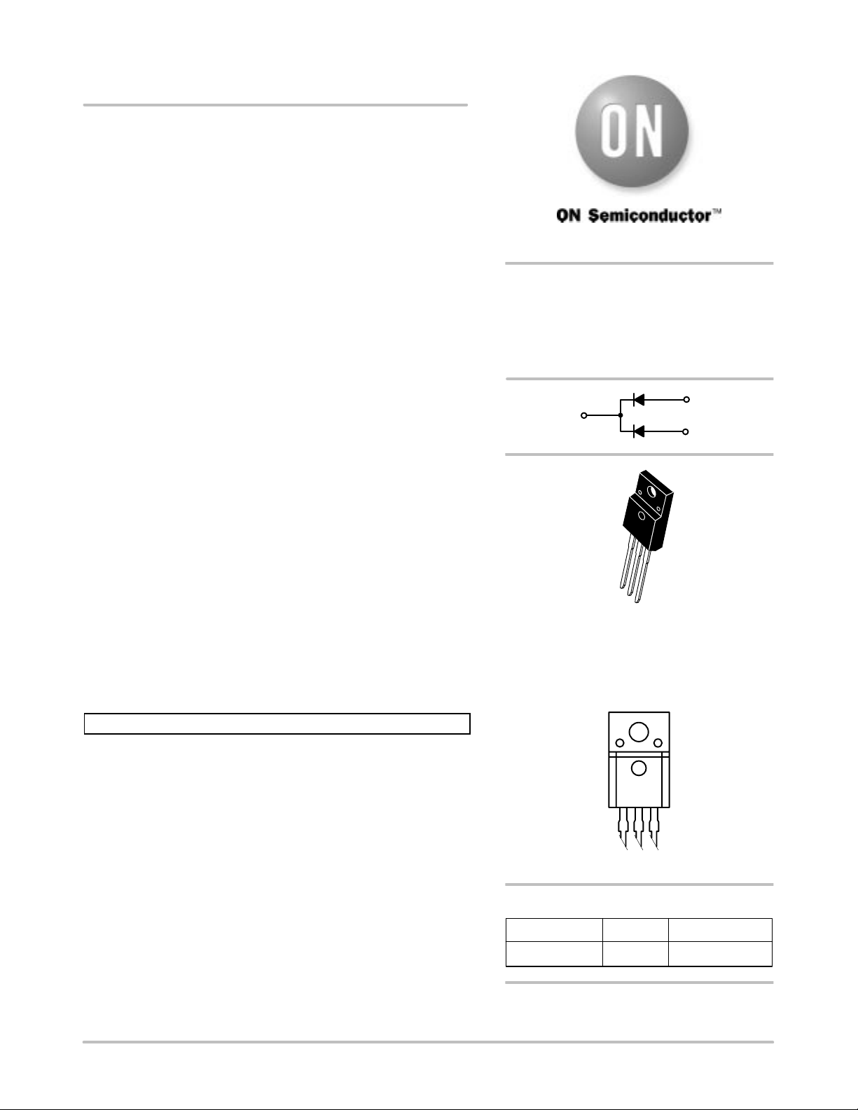
ISOLATED TO–220
CASE 221D
STYLE 3
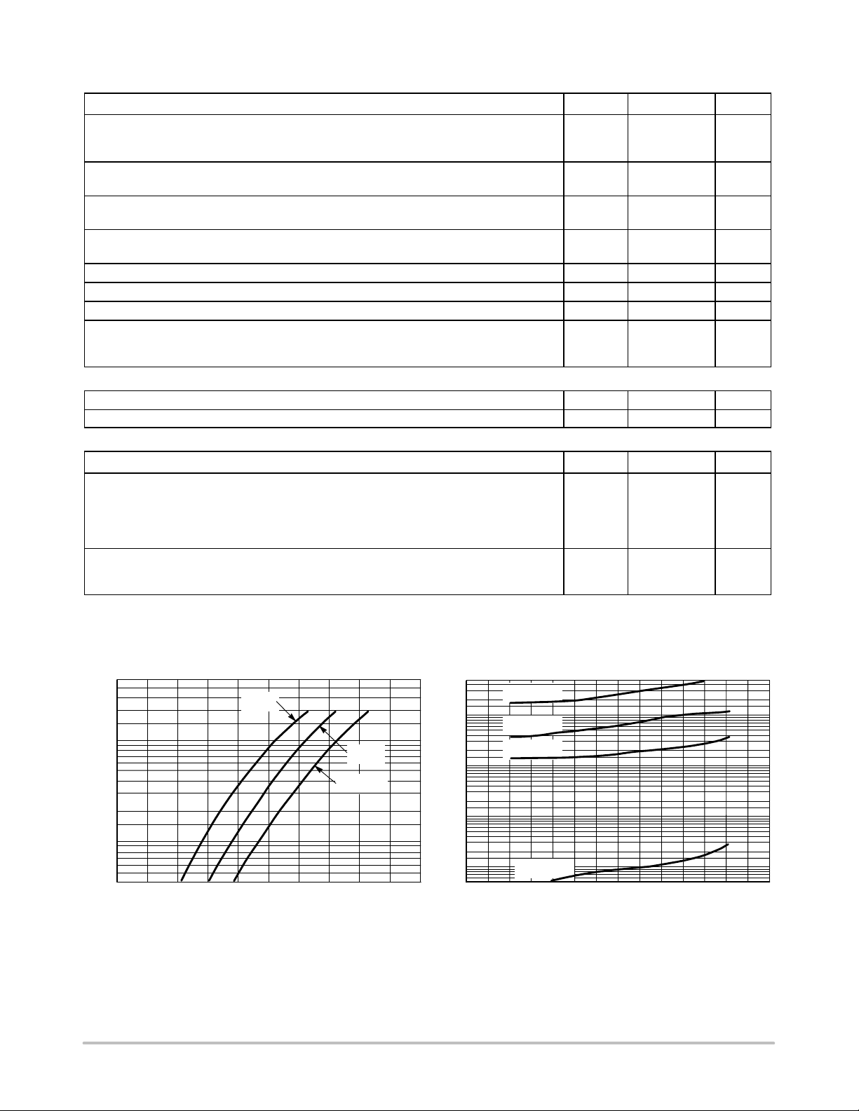
MARKING DIAGRAM
B20100
B20100= Device Code
ORDERING INFORMATION
Semiconductor Components Industries, LLC, 2000
October, 2000 – Rev. 2
Device Package Shipping
MBRF20100CT TO–220
Preferred devices are recommended choices for future use
and best overall value.
1 Publication Order Number:
50 Units/Rail
MBRF20100CT/D
MBRF20100CT
MAXIMUM RATINGS (Per Leg)
Rating Symbol Value Unit
Peak Repetitive Reverse Voltage
Working Peak Reverse Voltage
DC Blocking Voltage
Average Rectified Forward Current
(Rated V
), TC = 133°C Total Device
R
Peak Repetitive Forward Current
(Rated V
, Square Wave, 20 kHz), TC = 133°C
R
Non–repetitive Peak Surge Current
(Surge applied at rated load conditions halfwave, single phase, 60 Hz)
Peak Repetitive Reverse Surge Current (2.0 µs, 1.0 kHz) I
Operating Junction and Storage Temperature Range TJ, T
Voltage Rate of Change (Rated VR) dv/dt 10000 V/µs
RMS Isolation Voltage (t = 1.0 second, R.H. ≤ 30%, TA = 25°C) (Note 2.) Per Figure 3.
Per Figure 4. (Note 1.)
Per Figure 5.
THERMAL CHARACTERISTICS (Per Leg)
Maximum Thermal Resistance, Junction to Case R
Lead Temperature for Soldering Purposes: 1/8″ from Case for 5 Seconds T
ELECTRICAL CHARACTERISTICS (Per Leg)
Characteristic Symbol Max Unit
Maximum Instantaneous Forward Voltage (Note 3.)
(i
= 10 Amp, TC = 25°C)
F
(i
= 10 Amp, TC = 125°C)
F
(i
= 20 Amp, TC = 25°C)
F
(i
= 20 Amp, TC = 125°C)
F
Maximum Instantaneous Reverse Current (Note 3.)
(Rated DC Voltage, T
(Rated DC Voltage, T
1. UL Recognized mounting method is per Figure 4.
2. Proper strike and creepage distance must be provided.
3. Pulse Test: Pulse Width = 300 µs, Duty Cycle ≤ 2.0%
= 25°C)
C
= 125°C)
C
V
V
I
F(AV)
I
I
RRM
V
V
V
RRM
RWM
V
R
FRM
FSM
iso1
iso2
iso3
θ
JC
L
v
F
i
R
– 65 to +150 °C
stg
4500
3500
1500
100 Volts
10
20
20 Amps
150 Amps
0.5 Amp
3.5 °C/W
260 °C
0.85
0.75
0.95
0.85
0.15
150
Amps
Volts
Volts
mA
50
20
10
5.0
3.0
1.0
0.5
, INSTANTANEOUS FORWARD CURRENT (AMPS)
F
i
0
150°C
100°C
T
= 25°C
J
0.1 0.2 0.3 0.4 0.5 0.6 0.7 0.8 0.9 1.0
v
, INSTANTANEOUS VOLTAGE (VOLTS)
F
Figure 1. Typical Forward Voltage Per Diode
http://onsemi.com
T
= 150°C
J
10
T
= 125°C
J
T
= 100°C
J
1.0
0.1
, REVERSE CURRENT (mA)
R
I
0.01
T
= 25°C
J
120100806040200
V
, REVERSE VOLTAGE (VOLTS)
R
Figure 2. Typical Reverse Current Per Diode
2

MBRF20100CT
TEST CONDITIONS FOR ISOLATION TESTS*
MOUNTED
CLIP
Figure 3. Clip Mounting Position
for Isolation Test Number 1
* Measurement made between leads and heatsink with all leads shorted together.
FULLY ISOLATED
PACKAGE
CLIP
LEADS
HEATSINK
0.110″ MIN
Figure 4. Clip Mounting Position
FULLY ISOLATED
for Isolation Test Number 2
MOUNTING INFORMATION**
4-40 SCREW
PLAIN WASHER
MOUNTED
PACKAGE
0.107″ MIN
LEADS
HEATSINK
MOUNTED
FULLY ISOLATED
PACKAGE
Figure 5. Screw Mounting Position
for Isolation Test Number 3
CLIP
0.107″ MIN
LEADS
HEATSINK
HEATSINK
COMPRESSION WASHER
NUT
HEATSINK
6a. Screw–Mounted 6b. Clip–Mounted
Figure 6. T ypical Mounting Techniques
Laboratory tests on a limited number of samples indicate, when using the screw and compression washer mounting
technique, a screw torque of 6 to 8 in.lbs is sufficient to provide maximum power dissipation capability. The compression
washer helps to maintain a constant pressure on the package over time and during large temperature excursions.
Destructive laboratory tests show that using a hex head 4–40 screw , without washers, and applying a torque in excess of 20
.
in
lbs will cause the plastic to crack around the mounting hole, resulting in a loss of isolation capability.
Additional tests on slotted 4–40 screws indicate that the screw slot fails between 15 to 20 i n.lbs without adversely affecting
the package. However, in order to positively ensure the package integrity of the fully isolated device, ON Semiconductor does
not recommend exceeding 10 in.lbs of mounting torque under any mounting conditions.
**For more information about mounting power semiconductors see Application Note AN1040.
http://onsemi.com
3

MBRF20100CT
PACKAGE DIMENSIONS
TO–220
FULLPAK
CASE 221D–02
ISSUE D
SEATING
–T–
PLANE
F
–B–
Q
C
S
U
A
123
H
G
N
–Y–
J
R
K
L
D
3 PL
M
M
0.25 (0.010) Y
B
SWITCHMODE is a trademark of Semiconductor Components Industries, LLC.
NOTES:
1. DIMENSIONING AND TOLERANCING PER ANSI
Y14.5M, 1982.
2. CONTROLLING DIMENSION: INCH.
INCHES
DIMAMIN MAX MIN MAX
0.621 0.629 15.78 15.97
B 0.394 0.402 10.01 10.21
C 0.181 0.189 4.60 4.80
D 0.026 0.034 0.67 0.86
F 0.121 0.129 3.08 3.27
G 0.100 BSC 2.54 BSC
H 0.123 0.129 3.13 3.27
J 0.018 0.025 0.46 0.64
K 0.500 0.562 12.70 14.27
L 0.045 0.060 1.14 1.52
N 0.200 BSC 5.08 BSC
Q 0.126 0.134 3.21 3.40
R 0.107 0.111 2.72 2.81
S 0.096 0.104 2.44 2.64
U 0.259 0.267 6.58 6.78
STYLE 3:
PIN 1. ANODE
2. CATHODE
3. ANODE
MILLIMETERS
ON Semiconductor and are trademarks of Semiconductor Components Industries, LLC (SCILLC). SCILLC reserves the right to make changes
without further notice to any products herein. SCILLC makes no warranty, representation or guarantee regarding the suitability of its products for any particular
purpose, nor does SCILLC assume any liability arising out of the application or use of any product or circuit, and specifically disclaims any and all liability,
including without limitation special, consequential or incidental damages. “Typical” parameters which may be provided in SCILLC data sheets and/or
specifications can and do vary in different applications and actual performance may vary over time. All operating parameters, including “Typicals” must be
validated for each customer application by customer’s technical experts. SCILLC does not convey any license under its patent rights nor the rights of others.
SCILLC products are not designed, intended, or authorized for use as components in systems intended for surgical implant into the body, or other applications
intended to support or sustain life, or for any other application in which the failure of the SCILLC product could create a situation where personal injury or
death may occur. Should Buyer purchase or use SCILLC products for any such unintended or unauthorized application, Buyer shall indemnify and hold
SCILLC and its officers, employees, subsidiaries, affiliates, and distributors harmless against all claims, costs, damages, and expenses, and reasonable
attorney fees arising out of, directly or indirectly, any claim of personal injury or death associated with such unintended or unauthorized use, even if such claim
alleges that SCILLC was negligent regarding the design or manufacture of the part. SCILLC is an Equal Opportunity/Affirmative Action Employer.
PUBLICATION ORDERING INFORMATION
NORTH AMERICA Literature Fulfillment:
Literature Distribution Center for ON Semiconductor
P.O. Box 5163, Denver, Colorado 80217 USA
Phone: 303–675–2175 or 800–344–3860 Toll Free USA/Canada
Fax: 303–675–2176 or 800–344–3867 Toll Free USA/Canada
Email: ONlit@hibbertco.com
Fax Response Line: 303–675–2167 or 800–344–3810 Toll Free USA/Canada
N. American Technical Support: 800–282–9855 Toll Free USA/Canada
EUROPE: LDC for ON Semiconductor – European Support
German Phone: (+1) 303–308–7140 (Mon–Fri 2:30pm to 7:00pm CET)
Email: ONlit–german@hibbertco.com
French Phone: (+1) 303–308–7141 (Mon–Fri 2:00pm to 7:00pm CET)
Email: ONlit–french@hibbertco.com
English Phone: (+1) 303–308–7142 (Mon–Fri 12:00pm to 5:00pm GMT)
Email: ONlit@hibbertco.com
EUROPEAN TOLL–FREE ACCESS*: 00–800–4422–3781
*Available from Germany, France, Italy, UK, Ireland
CENTRAL/SOUTH AMERICA:
Spanish Phone: 303–308–7143 (Mon–Fri 8:00am to 5:00pm MST)
Email: ONlit–spanish@hibbertco.com
Toll–Free from Mexico: Dial 01–800–288–2872 for Access –
then Dial 866–297–9322
ASIA/PACIFIC: LDC for ON Semiconductor – Asia Support
Phone: 303–675–2121 (Tue–Fri 9:00am to 1:00pm, Hong Kong Time)
Toll Free from Hong Kong & Singapore:
001–800–4422–3781
Email: ONlit–asia@hibbertco.com
JAPAN: ON Semiconductor, Japan Customer Focus Center
4–32–1 Nishi–Gotanda, Shinagawa–ku, Tokyo, Japan 141–0031
Phone: 81–3–5740–2700
Email: r14525@onsemi.com
ON Semiconductor Website: http://onsemi.com
For additional information, please contact your local
Sales Representative.
http://onsemi.com
4
MBRF20100CT/D

 Loading...