

Omron CJ1W-AD041-V1, CS1W-DA08C, CJ1W-AD081-V1, CJ1W-DA021, CJ1W-DA041 Operation Manual
...Page 1

Cat. No. W345-E1-08
SYSMAC CS/CJ Series
CS1W-AD041-V1/AD081-V1/AD161
CS1W-DA041/DA08V/DA08C
CS1W-MAD44
CJ1W-AD041-V1/AD081-V1
CJ1W-DA021/DA041/DA08V/DA08C
CJ1W-MAD42
Analog I/O Units
OPERATION MANUAL
Page 2

SYSMAC CS/CJ Series
CS1W-AD041-V1/AD081-V1/AD161
CS1W-DA041/DA08V/DA08C
CS1W-MAD44
CJ1W-AD041-V1/AD081-V1
CJ1W-DA021/DA041/DA08V/DA08C
CJ1W-MAD42
Analog I/O Units
Operation Manual
Revised July 2005
Page 3

iv
Page 4

Notice:
OMRON products are manufactured for use according to proper procedures by a qualified operator
and only for the purposes described in this manual.
The following conventions are used to indicate and classify precautions in this manual. Always heed
the information provided with them. Failure to heed precautions can result in injury to people or damage to property.
!DANGER Indicates an imminently hazardous situation which, if not avoided, will result in death or
serious injury. Additionally, there may be severe property damage.
!WARNING Indicates a potentially hazardous situation which, if not avoided, could result in death or
serious injury. Additionally, there may be severe property damage.
!Caution Indicates a potentially hazardous situation which, if not avoided, may result in minor or
moderate injury, or property damage.
OMRON Product References
All OMRON products are capitalized in this manual. The word “Unit” is also capitalized when it refers to
an OMRON product, regardless of whether or not it appears in the proper name of the product.
The abbreviation “Ch,” which appears in some displays and on some OMRON products, often means
“word” and is abbreviated “Wd” in documentation in this sense.
The abbreviation “PLC” means Programmable Controller. “PC” is used, however, in some Programming Device displays to mean Programmable Controller.
Visual Aids
The following headings appear in the left column of the manual to help you locate different types of
information.
OMRON, 1999
All rights reserved. No part of this publication may be reproduced, stored in a retrieval system, or transmitted, in any form, or
by any means, mechanical, electronic, photocopying, recording, or otherwise, without the prior written permission of
OMRON.
No patent liability is assumed with respect to the use of the information contained herein. Moreover, because OMRON is constantly striving to improve its high-quality products, the information contained in this manual is subject to change without
notice. Every precaution has been taken in the preparation of this manual. Nevertheless, OMRON assumes no responsibility
for errors or omissions. Neither is any liability assumed for damages resulting from the use of the information contained in
this publication.
Note Indicates information of particular interest for efficient and convenient opera-
tion of the product.
1,2,3...
1. Indicates lists of one sort or another, such as procedures, checklists, etc.
v
Page 5

vi
Page 6

TABLE OF CONTENTS
PRECAUTIONS . . . . . . . . . . . . . . . . . . . . . . . . . . . . . . . . xvii
1 Intended Audience. . . . . . . . . . . . . . . . . . . . . . . . . . . . . . . . . . . . . . . . . . . . . . . . . xviii
2 General Precautions. . . . . . . . . . . . . . . . . . . . . . . . . . . . . . . . . . . . . . . . . . . . . . . . xviii
3 Safety Precautions . . . . . . . . . . . . . . . . . . . . . . . . . . . . . . . . . . . . . . . . . . . . . . . . . xviii
4 Operating Environment Precautions . . . . . . . . . . . . . . . . . . . . . . . . . . . . . . . . . . . xix
5 Application Precautions. . . . . . . . . . . . . . . . . . . . . . . . . . . . . . . . . . . . . . . . . . . . . xx
6 EC Directives. . . . . . . . . . . . . . . . . . . . . . . . . . . . . . . . . . . . . . . . . . . . . . . . . . . . . xxi
7 Other Applicable Directives . . . . . . . . . . . . . . . . . . . . . . . . . . . . . . . . . . . . . . . . . xxii
8 Precautions for the C200H-AD003, C200H-DA003/004, and C200H-MAD01. . xxii
9 Changes to the CJ1W-DA08V/08C and CJ1W-MAD42 . . . . . . . . . . . . . . . . . . . . xxiii
SECTION 1
System Design . . . . . . . . . . . . . . . . . . . . . . . . . . . . . . . . . . 1
1-1 Features and Functions . . . . . . . . . . . . . . . . . . . . . . . . . . . . . . . . . . . . . . . . . . . . . 2
1-2 Basic Configuration. . . . . . . . . . . . . . . . . . . . . . . . . . . . . . . . . . . . . . . . . . . . . . . . 7
1-3 Function Applications . . . . . . . . . . . . . . . . . . . . . . . . . . . . . . . . . . . . . . . . . . . . . . 12
SECTION 2
CS-series Analog Input Units . . . . . . . . . . . . . . . . . . . . . . 13
2-1 Specifications. . . . . . . . . . . . . . . . . . . . . . . . . . . . . . . . . . . . . . . . . . . . . . . . . . . . . 14
2-2 Operating Procedure . . . . . . . . . . . . . . . . . . . . . . . . . . . . . . . . . . . . . . . . . . . . . . . 20
2-3 Components and Switch Settings . . . . . . . . . . . . . . . . . . . . . . . . . . . . . . . . . . . . . 27
2-4 Wiring . . . . . . . . . . . . . . . . . . . . . . . . . . . . . . . . . . . . . . . . . . . . . . . . . . . . . . . . . . 32
2-5 Exchanging Data with the CPU Unit. . . . . . . . . . . . . . . . . . . . . . . . . . . . . . . . . . . 39
2-6 Analog Input Functions and Operating Procedures. . . . . . . . . . . . . . . . . . . . . . . . 52
2-7 Adjusting Offset and Gain . . . . . . . . . . . . . . . . . . . . . . . . . . . . . . . . . . . . . . . . . . . 60
2-8 Handling Errors and Alarms . . . . . . . . . . . . . . . . . . . . . . . . . . . . . . . . . . . . . . . . . 69
SECTION 3
CJ-series Analog Input Units . . . . . . . . . . . . . . . . . . . . . . 77
3-1 Specifications. . . . . . . . . . . . . . . . . . . . . . . . . . . . . . . . . . . . . . . . . . . . . . . . . . . . . 78
3-2 Operating Procedure . . . . . . . . . . . . . . . . . . . . . . . . . . . . . . . . . . . . . . . . . . . . . . . 83
3-3 Components and Switch Settings . . . . . . . . . . . . . . . . . . . . . . . . . . . . . . . . . . . . . 89
3-4 Wiring . . . . . . . . . . . . . . . . . . . . . . . . . . . . . . . . . . . . . . . . . . . . . . . . . . . . . . . . . . 93
3-5 Exchanging Data with the CPU Unit. . . . . . . . . . . . . . . . . . . . . . . . . . . . . . . . . . . 97
3-6 Analog Input Functions and Operating Procedures. . . . . . . . . . . . . . . . . . . . . . . . 104
3-7 Adjusting Offset and Gain . . . . . . . . . . . . . . . . . . . . . . . . . . . . . . . . . . . . . . . . . . . 112
3-8 Handling Errors and Alarms . . . . . . . . . . . . . . . . . . . . . . . . . . . . . . . . . . . . . . . . . 120
vii
Page 7

TABLE OF CONTENTS
SECTION 4
CS-series Analog Output Units . . . . . . . . . . . . . . . . . . . . 125
4-1 Specifications. . . . . . . . . . . . . . . . . . . . . . . . . . . . . . . . . . . . . . . . . . . . . . . . . . . . . 126
4-2 Operating Procedure . . . . . . . . . . . . . . . . . . . . . . . . . . . . . . . . . . . . . . . . . . . . . . . 130
4-3 Components and Switch Settings . . . . . . . . . . . . . . . . . . . . . . . . . . . . . . . . . . . . . 136
4-4 Wiring . . . . . . . . . . . . . . . . . . . . . . . . . . . . . . . . . . . . . . . . . . . . . . . . . . . . . . . . . . 139
4-5 Exchanging Data with the CPU Unit. . . . . . . . . . . . . . . . . . . . . . . . . . . . . . . . . . . 142
4-6 Analog Output Functions and Operating Procedures . . . . . . . . . . . . . . . . . . . . . . 149
4-7 Adjusting Offset and Gain . . . . . . . . . . . . . . . . . . . . . . . . . . . . . . . . . . . . . . . . . . . 153
4-8 Handling Errors and Alarms . . . . . . . . . . . . . . . . . . . . . . . . . . . . . . . . . . . . . . . . . 163
SECTION 5
CJ-series Analog Output Unit . . . . . . . . . . . . . . . . . . . . . 169
5-1 Specifications. . . . . . . . . . . . . . . . . . . . . . . . . . . . . . . . . . . . . . . . . . . . . . . . . . . . . 170
5-2 Operating Procedure . . . . . . . . . . . . . . . . . . . . . . . . . . . . . . . . . . . . . . . . . . . . . . . 174
5-3 Components and Switch Settings . . . . . . . . . . . . . . . . . . . . . . . . . . . . . . . . . . . . . 182
5-4 Wiring . . . . . . . . . . . . . . . . . . . . . . . . . . . . . . . . . . . . . . . . . . . . . . . . . . . . . . . . . . 184
5-5 Exchanging Data with the CPU Unit. . . . . . . . . . . . . . . . . . . . . . . . . . . . . . . . . . . 188
5-6 Analog Output Functions and Operating Procedures . . . . . . . . . . . . . . . . . . . . . . 197
5-7 Adjusting Offset and Gain . . . . . . . . . . . . . . . . . . . . . . . . . . . . . . . . . . . . . . . . . . . 204
5-8 Handling Errors and Alarms . . . . . . . . . . . . . . . . . . . . . . . . . . . . . . . . . . . . . . . . . 215
SECTION 6
CS-series Analog I/O Unit . . . . . . . . . . . . . . . . . . . . . . . . 221
6-1 Specifications. . . . . . . . . . . . . . . . . . . . . . . . . . . . . . . . . . . . . . . . . . . . . . . . . . . . . 222
6-2 Operating Procedure . . . . . . . . . . . . . . . . . . . . . . . . . . . . . . . . . . . . . . . . . . . . . . . 230
6-3 Components and Switch Settings . . . . . . . . . . . . . . . . . . . . . . . . . . . . . . . . . . . . . 237
6-4 Wiring . . . . . . . . . . . . . . . . . . . . . . . . . . . . . . . . . . . . . . . . . . . . . . . . . . . . . . . . . . 240
6-5 Exchanging Data with the CPU Unit. . . . . . . . . . . . . . . . . . . . . . . . . . . . . . . . . . . 244
6-6 Analog Input Functions and Operating Procedures. . . . . . . . . . . . . . . . . . . . . . . . 252
6-7 Analog Output Functions and Operating Procedures . . . . . . . . . . . . . . . . . . . . . . 259
6-8 Ratio Conversion Function . . . . . . . . . . . . . . . . . . . . . . . . . . . . . . . . . . . . . . . . . . 262
6-9 Adjusting Offset and Gain . . . . . . . . . . . . . . . . . . . . . . . . . . . . . . . . . . . . . . . . . . . 265
6-10 Handling Errors and Alarms . . . . . . . . . . . . . . . . . . . . . . . . . . . . . . . . . . . . . . . . . 281
viii
Page 8

TABLE OF CONTENTS
SECTION 7
CJ-series Analog I/O Unit. . . . . . . . . . . . . . . . . . . . . . . . . 287
7-1 Specifications. . . . . . . . . . . . . . . . . . . . . . . . . . . . . . . . . . . . . . . . . . . . . . . . . . . . . 288
7-2 Operating Procedure . . . . . . . . . . . . . . . . . . . . . . . . . . . . . . . . . . . . . . . . . . . . . . . 295
7-3 Components and Switch Settings . . . . . . . . . . . . . . . . . . . . . . . . . . . . . . . . . . . . . 302
7-4 Wiring . . . . . . . . . . . . . . . . . . . . . . . . . . . . . . . . . . . . . . . . . . . . . . . . . . . . . . . . . . 305
7-5 Exchanging Data with the CPU Unit. . . . . . . . . . . . . . . . . . . . . . . . . . . . . . . . . . . 309
7-6 Analog Input Functions and Operating Procedures. . . . . . . . . . . . . . . . . . . . . . . . 318
7-7 Analog Output Functions and Operating Procedures . . . . . . . . . . . . . . . . . . . . . . 327
7-8 Ratio Conversion Function . . . . . . . . . . . . . . . . . . . . . . . . . . . . . . . . . . . . . . . . . . 333
7-9 Adjusting Offset and Gain . . . . . . . . . . . . . . . . . . . . . . . . . . . . . . . . . . . . . . . . . . . 336
7-10 Handling Errors and Alarms . . . . . . . . . . . . . . . . . . . . . . . . . . . . . . . . . . . . . . . . . 352
Appendices
A Dimensions . . . . . . . . . . . . . . . . . . . . . . . . . . . . . . . . . . . . . . . . . . . . . . . . . . . . . . 359
B Sample Programs . . . . . . . . . . . . . . . . . . . . . . . . . . . . . . . . . . . . . . . . . . . . . . . . . 363
C Data Memory Coding Sheets . . . . . . . . . . . . . . . . . . . . . . . . . . . . . . . . . . . . . . . . 373
Index . . . . . . . . . . . . . . . . . . . . . . . . . . . . . . . . . . . . . . . . . . 395
Revision History . . . . . . . . . . . . . . . . . . . . . . . . . . . . . . . . 401
ix
Page 9

TABLE OF CONTENTS
x
Page 10

About this Manual:
This manual describes the installation and operation of the CS1W-AD041-V1, CS1W-AD081-V1,
CS1W-AD161, CJ1W-AD041-V1, and CJ1W-AD081-V1 Analog Input Units; the CS1W-DA041, CS1WDA08V, CS1W-DA08C, CJ1W-DA021, CJ1W-DA041, CJ1W-DA08V, and CJ1W-DA08C Analog Output
Units; and the CS1W-MAD44 and CJ1W-MAD42 Analog I/O Units. This manual includes the sections
described below.
The input function of CS/CJ-series Analog I/O Units converts analog sensor output to the digital format
and transmits it to CS/CJ-series PLCs. The output function converts digital data from the PLC to the
analog format for output.
Please read this manual and the other manuals related to the CS/CJ-series Analog I/O Units carefully
and be sure you understand the information provided before attempting to install and operate the
Units. The manuals used with the CS/CJ-series Analog I/O Units are listed in the following table. The
suffixes have been omitted from the catalog numbers. Be sure you are using the most recent version
for your area.
Name Cat. No. Contents
SYSMAC CS-series
CS1G/H-CPU@@-EV1, CS1G/H-CPU@@H
Programmable Controllers Operation Manual
SYSMAC CS Series
CS1D-CPU@@H CPU Units, CS1D-CPU@@S CPU Units,
CS1D-DPL01 Duplex Unit, CS1D-PA/PD@@@ Power
Supply Unit
CS1D Duplex System Operation Manual
SYSMAC CJ-series
CJ1G-CPU@@, CJ1G/H-CPU@@H, CJ1M-CPU@@
Programmable Controllers Operation Manual
SYSMAC CS/CJ-series
CS1G/H-CPU@@-EV1, CS1G/H-CPU@@H, CJ1GCPU@@, CJ1G/H-CPU@@H, CJ1M-CPU@@
Programmable Controllers Programming Manual
SYSMAC CS/CJ-series
CS1G/H-CPU@@-EV1, CS1G/H-CPU@@H, CJ1GCPU@@, CJ1G/H-CPU@@H, CJ1M-CPU@@
Programmable Controllers Instructions Reference Manual
SYSMAC WS02-CXPC1-EV50
CX-Programmer Ver. 5.0 Operation Manual
SYSMAC CS/CJ-series
CQM1H-PRO01-E, CQM1-PRO01-E, C200H-PRO27-E
Programming Consoles Operation Manual
W339 Describes the installation and operation
of the CS-series PLCs.
W405 Provides an outline of and describes the
design, installation, maintenance, and
other basic operations for a Duplex System based on CS1D CPU Units.
W393 Describes the installation and operation
of the CJ-series PLCs.
W394 Describes the programming methods
required to use the functions of the CS/
CJ-series PLCs.
W340 Describes the ladder diagram program-
ming instructions supported by CS/CJseries PLCs.
W437 Provides information on how to use the
CX-Programmer, a programming device
that supports the CS/CJ-series PLCs.
W341 Provides information on how to program
and operate CS/CJ-series PLCs using a
Programming Console.
xi
Page 11

Section 1 describes the features and system configurations of the CS/CJ-series Analog I/O Unit.
Section 2 explains how to use the CS1W-AD041-V1/081-V1/161 Analog Input Units.
Section 3 explains how to use the CJ1W-AD041-V1/081-V1 Analog Input Units.
Section 4 explains how to use the CS1W-DA041/08V/08C Analog Output Units.
Section 5 explains how to use the CJ1W-DA021/041/08V/08C Analog Output Units.
Section 6 explains how to use the CS1W-MAD44 Analog I/O Unit.
Section 7 explains how to use the CJ1W-MAD42 Analog I/O Unit.
Appendix A provides details on dimensions.
Appendix B gives programming examples.
Appendix C provides data memory coding sheets.
!WARNING Failure to read and understand the information provided in this manual may result in per-
sonal injury or death, damage to the product, or product failure. Please read each section
in its entirety and be sure you understand the information provided in the section and
related sections before attempting any of the procedures or operations given.
xii
Page 12

Read and Understand this Manual
Please read and understand this manual before using the product. Please consult your OMRON
representative if you have any questions or comments.
Warranty and Limitations of Liability
WARRANTY
OMRON's exclusive warranty is that the products are free from defects in materials and workmanship for a
period of one year (or other period if specified) from date of sale by OMRON.
OMRON MAKES NO WARRANTY OR REPRESENTATION, EXPRESS OR IMPLIED, REGARDING NONINFRINGEMENT, MERCHANTABILITY, OR FITNESS FOR PARTICULAR PURPOSE OF THE
PRODUCTS. ANY BUYER OR USER ACKNOWLEDGES THAT THE BUYER OR USER ALONE HAS
DETERMINED THAT THE PRODUCTS WILL SUITABLY MEET THE REQUIREMENTS OF THEIR
INTENDED USE. OMRON DISCLAIMS ALL OTHER WARRANTIES, EXPRESS OR IMPLIED.
LIMITATIONS OF LIABILITY
OMRON SHALL NOT BE RESPONSIBLE FOR SPECIAL, INDIRECT, OR CONSEQUENTIAL DAMAGES,
LOSS OF PROFITS OR COMMERCIAL LOSS IN ANY WAY CONNECTED WITH THE PRODUCTS,
WHETHER SUCH CLAIM IS BASED ON CONTRACT, WARRANTY, NEGLIGENCE, OR STRICT
LIABILITY.
In no event shall the responsibility of OMRON for any act exceed the individual price of the product on which
liability is asserted.
IN NO EVENT SHALL OMRON BE RESPONSIBLE FOR WARRANTY, REPAIR, OR OTHER CLAIMS
REGARDING THE PRODUCTS UNLESS OMRON'S ANALYSIS CONFIRMS THAT THE PRODUCTS
WERE PROPERLY HANDLED, STORED, INSTALLED, AND MAINTAINED AND NOT SUBJECT TO
CONTAMINATION, ABUSE, MISUSE, OR INAPPROPRIATE MODIFICATION OR REPAIR.
xiii
Page 13

Application Considerations
SUITABILITY FOR USE
OMRON shall not be responsible for conformity with any standards, codes, or regulations that apply to the
combination of products in the customer's application or use of the products.
At the customer's request, OMRON will provide applicable third party certification documents identifying
ratings and limitations of use that apply to the products. This information by itself is not sufficient for a
complete determination of the suitability of the products in combination with the end product, machine,
system, or other application or use.
The following are some examples of applications for which particular attention must be given. This is not
intended to be an exhaustive list of all possible uses of the products, nor is it intended to imply that the uses
listed may be suitable for the products:
• Outdoor use, uses involving potential chemical contamination or electrical interference, or conditions or
uses not described in this manual.
• Nuclear energy control systems, combustion systems, railroad systems, aviation systems, medical
equipment, amusement machines, vehicles, safety equipment, and installations subject to separate
industry or government regulations.
• Systems, machines, and equipment that could present a risk to life or property.
Please know and observe all prohibitions of use applicable to the products.
NEVER USE THE PRODUCTS FOR AN APPLICATION INVOLVING SERIOUS RISK TO LIFE OR
PROPERTY WITHOUT ENSURING THAT THE SYSTEM AS A WHOLE HAS BEEN DESIGNED TO
ADDRESS THE RISKS, AND THAT THE OMRON PRODUCTS ARE PROPERLY RATED AND
INSTALLED FOR THE INTENDED USE WITHIN THE OVERALL EQUIPMENT OR SYSTEM.
PROGRAMMABLE PRODUCTS
OMRON shall not be responsible for the user's programming of a programmable product, or any
consequence thereof.
xiv
Page 14

Disclaimers
CHANGE IN SPECIFICATIONS
Product specifications and accessories may be changed at any time based on improvements and other
reasons.
It is our practice to change model numbers when published ratings or features are changed, or when
significant construction changes are made. However, some specifications of the products may be changed
without any notice. When in doubt, special model numbers may be assigned to fix or establish key
specifications for your application on your request. Please consult with your OMRON representative at any
time to confirm actual specifications of purchased products.
DIMENSIONS AND WEIGHTS
Dimensions and weights are nominal and are not to be used for manufacturing purposes, even when
tolerances are shown.
PERFORMANCE DATA
Performance data given in this manual is provided as a guide for the user in determining suitability and does
not constitute a warranty. It may represent the result of OMRON's test conditions, and the users must
correlate it to actual application requirements. Actual performance is subject to the OMRON Warranty and
Limitations of Liability.
ERRORS AND OMISSIONS
The information in this manual has been carefully checked and is believed to be accurate; however, no
responsibility is assumed for clerical, typographical, or proofreading errors, or omissions.
xv
Page 15

xvi
Page 16

PRECAUTIONS
This section provides general precautions for using the Programmable Controller (PLC) and Analog I/O Units.
The information contained in this section is important for the safe and reliable application of the Analog I/O Unit.
You must read this section and understand the information contained before attempting to set up or operate a PLC
system and Analog I/O Unit.
1 Intended Audience . . . . . . . . . . . . . . . . . . . . . . . . . . . . . . . . . . . . . . . . . . . . . xviii
2 General Precautions . . . . . . . . . . . . . . . . . . . . . . . . . . . . . . . . . . . . . . . . . . . . xviii
3 Safety Precautions. . . . . . . . . . . . . . . . . . . . . . . . . . . . . . . . . . . . . . . . . . . . . . xviii
4 Operating Environment Precautions . . . . . . . . . . . . . . . . . . . . . . . . . . . . . . . . xix
5 Application Precautions . . . . . . . . . . . . . . . . . . . . . . . . . . . . . . . . . . . . . . . . . xx
6 EC Directives . . . . . . . . . . . . . . . . . . . . . . . . . . . . . . . . . . . . . . . . . . . . . . . . . xxi
7 Other Applicable Directives . . . . . . . . . . . . . . . . . . . . . . . . . . . . . . . . . . . . . . xxii
8 Precautions for the C200H-AD003, C200H-DA003/004, and C200H-MAD01 xxii
9 Changes to the CJ1W-DA08V/08C and CJ1W-MAD42 . . . . . . . . . . . . . . . . xxiii
xvii
Page 17

Intended Audience 1
1 Intended Audience
This manual is intended for the following personnel, who must also have
knowledge of electrical systems (an electrical engineer or the equivalent).
• Personnel in charge of installing FA systems
• Personnel in charge of designing FA systems
• Personnel in charge of managing FA systems and facilities
2 General Precautions
The user must operate the product according to the performance specifications described in the operation manuals.
Before using the product under conditions which are not described in the
manual or applying the product to nuclear control systems, railroad systems,
aviation systems, vehicles, combustion systems, medical equipment, amusement machines, safety equipment, and other systems, machines, and equipment that may have a serious influence on lives and property if used
improperly, consult your OMRON representative.
Make sure that the ratings and performance characteristics of the product are
sufficient for the systems, machines, and equipment, and be sure to provide
the systems, machines, and equipment with double safety mechanisms.
This manual provides information for programming and operating OMRON
Analog I/O Units. Be sure to read this manual before attempting to use the
software and keep this manual close at hand for reference during operation.
!WARNING It is extremely important that a PLC and all PLC Units be used for the speci-
fied purpose and under the specified conditions, especially in applications that
can directly or indirectly affect human life. You must consult with your OMRON
representative before applying a PLC System to the above-mentioned applications.
3 Safety Precautions
!WARNING Do not attempt to take any Unit apart while power is being supplied. Doing so
may result in electric shock.
!WARNING Do not touch any of the terminals or terminal blocks while power is being sup-
plied. Doing so may result in electric shock.
!WARNING Provide safety measures in external circuits (i.e., not in the Programmable
Controller), including the following items, in order to ensure safety in the system if an abnormality occurs due to malfunction of the PLC or another external factor affecting the PLC operation. Not doing so may result in serious
accidents.
• Emergency stop circuits, interlock circuits, limit circuits, and similar safety
measures must be provided in external control circuits.
• The PLC will turn OFF all outputs when its self-diagnosis function detects
any error or when a severe failure alarm (FALS) instruction is executed.
As a countermeasure for such errors, external safety measures must be
provided to ensure safety in the system.
xviii
Page 18

Operating Environment Precautions 4
• The PLC outputs may remain ON or OFF due to deposition or burning of
the output relays or destruction of the output transistors. As a countermeasure for such problems, external safety measures must be provided
to ensure safety in the system.
!WARNING When the 24-VDC output (service power supply to the PLC) is overloaded or
short-circuited, the voltage may drop and result in the outputs being turned
OFF. As a countermeasure for such problems, external safety measures must
be provided to ensure safety in the system.
!Caution When wiring crossovers between terminals, the total current for both terminals
will flow in the line. Check the current capacities of all wires before wiring
crossovers.
!Caution Tighten the screws on the terminal block of the AC Power Supply Unit to the
torque specified in the operation manual. The loose screws may result in
burning or malfunction.
!Caution Execute online edit only after confirming that no adverse effects will be
caused by extending the cycle time. Otherwise, the input signals may not be
readable.
4 Operating Environment Precautions
!Caution Do not operate the control system in the following places:
• Locations subject to direct sunlight.
• Locations subject to temperatures or humidity outside the range specified
in the specifications.
• Locations subject to condensation as the result of severe changes in temperature.
• Locations subject to corrosive or flammable gases.
• Locations subject to dust (especially iron dust) or salts.
• Locations subject to exposure to water, oil, or chemicals.
• Locations subject to shock or vibration.
!Caution Take appropriate and sufficient countermeasures when installing systems in
the following locations:
• Locations subject to static electricity or other forms of noise.
• Locations subject to strong electromagnetic fields.
• Locations subject to possible exposure to radioactivity.
• Locations close to power supplies.
!Caution The operating environment of the PLC System can have a large effect on the
longevity and reliability of the system. Improper operating environments can
lead to malfunction, failure, and other unforeseeable problems with the PLC
System. Be sure that the operating environment is within the specified conditions at installation and remains within the specified conditions during the life
of the system.
xix
Page 19

Application Precautions 5
5 Application Precautions
Observe the following precautions when using the PLC.
!WARNING Always heed these precautions. Failure to abide by the following precautions
could lead to serious or possibly fatal injury.
• Always connect to a class-3 ground (to 100
Units. Not connecting to a class-3 ground may result in electric shock.
• Always turn OFF the power supply to the PLC before attempting any of
the following. Not turning off the power supply may result in malfunction or
electric shock.
• Mounting or dismounting I/O Units, CPU Units, Memory Cassettes, or
any other Units.
• Assembling the Units.
• Setting DIP switch or rotary switches.
• Connecting or wiring the cables.
• Connecting or disconnecting the connectors.
!Caution Failure to abide by the following precautions could lead to faulty operation of
the PLC or the system, or could damage the PLC or PLC Units. Always heed
these precautions.
• Fail-safe measures must be taken by the customer to ensure safety in the
event of incorrect, missing, or abnormal signals caused by broken signal
lines, momentary power interruptions, or other causes.
• Always use the power supply voltage specified in this manual. An incorrect voltage may result in malfunction or burning.
• Take appropriate measures to ensure that the specified power with the
rated voltage and frequency is supplied. Be particularly careful in places
where the power supply is unstable. An incorrect power supply may result
in malfunction.
• Install external breakers and take other safety measures against short-circuiting in external wiring. Insufficient safety measures against short-circuiting may result in burning.
• Do not apply voltages to input sections in excess of the rated input voltage. Excess voltages may result in burning.
• Do not apply voltages or connect loads in excess of the maximum switching capacity to output sections. Excess voltage or loads may result in
burning.
• Be sure that all the mounting screws, terminal screws, and cable connector screws are tightened to the torque specified in the relevant manuals.
Incorrect tightening torque may result in malfunction.
• Wiring correctly, as indicated in this manual.
• Do not attempt to disassemble, repair, or modify any Units.
• Be sure to confirm that the DIP switch and the data memory (DM) are
properly set.
• Leave the label attached to the Unit when wiring. Removing the label may
result in malfunction.
Ω or less) when installing the
xx
Page 20

EC Directives 6
• Remove the labels after the completion of wiring to ensure proper heat
dissipation. Leaving the label attached may result in malfunction.
• Do not pull on cables and cords and do not bend them past their natural
bending radius.
• Do not place any heavy objects on cables or cords.
• Mount the Unit only after checking the terminal block completely.
• Be sure that the terminal blocks, Memory Units, expansion cables, and
other items with locking devices are properly locked into place. Improper
locking may result in malfunction.
• Check the user program for proper execution before actually running it on
the Unit. Not checking the program may result in an unexpected operation.
• Use crimp terminals for wiring. Do not connect bare stranded wires
directly to terminals. Connection of bare stranded wires may result in
burning.
• Double-check all the wiring before turning on the power supply. Incorrect
wiring may result in burning.
• Confirm that no adverse effect will occur in the system before attempting
any of the following. Not doing so may result in an unexpected operation.
• Changing the operating mode of the PLC (including the setting of the
startup operating mode).
• Force-setting/force-resetting any bit in memory.
• Changing the present value of any word or any set value in memory.
• Touch a grounded metal object to discharge static electricity from your
body before touching any Unit.
6 EC Directives
CS/CJ-series Units conform to EC Directives. For the system to conform to
EC Directives, however, the following precautions must be adhered to.
• CS/CJ-series Units must be installed within control panels.
• Use reinforced insulation or double insulation for the DC power supplies
used for the I/O power supplies.
• CS/CJ-series Units that meet EC Directives also meet the Common Emission Standard (EN61000-6-4). The measure necessary to ensure that
standards, such as the radiated emission standard (10 m), are met, however, will vary depending on the overall configuration of the control panel,
the other devices connected to the control panel, and wiring. You must
therefore confirm that EC Directives are met for the overall machine or
device.
xxi
Page 21

Other Applicable Directives 7
7 Other Applicable Directives
Applicable Directives
•EMC Directive
• Low Voltage Directive
EMC and Low Voltage Directives
EMC Directive
In order that OMRON products can be used with any machinery and in combination with other manufacturer’s equipment, the products themselves are
designed to comply with EMC standards (see note 1.), so that the assembled
machinery or device can then also easily comply with EMC standards.
Even if machinery and equipment complies with EMC standards before
assembly, this compliance may change depending on the device, the configuration of the control panel, and wiring, so OMRON cannot guarantee that particular system complies with the directive. You must therefore confirm that
EMC Directives are met for the overall machine or device.
Note EMC: One directive relating to Electro-Magnetic Compatibility
EMS: Electro-Magnetic Susceptibility Standard
CS Series: EN61131-2
CJ Series: EN61000-6-2
EMI: Electro-Magnetic Interference Standard EN61000-6-4
Common Emission Standard EN61000-6-4, radiated emission standard
(10 m)
Low Voltage Directive
The Low Voltage Directive provides that necessary safety standards are guaranteed for devices operating at voltages of 50 to 1,000 VAC or 75 to
1,500 VDC.
Conditions for
Conforming to EMC
Directive for CS/CJ-series
PLCs
The immunity test conditions for CJ-series Analog I/O Units are as follows:
Tot al Ac c u r a c y
CS1W-AD161: +4%/
CJ1W-DA021/DA041: +4%/
CJ1W-AD041-V1/AD081-V1: +3%/
CJ1W-DA08V/DA08C/MAD42: +4%/
−6%
−1%
−6%
−4%
8 Precautions for the C200H-AD003, C200H-DA003/004, and
C200H-MAD01
Note the following important differences between the CS-series Analog I/O
Units and the C200H Analog I/O Units.
Current Input Wiring
The CS1W-AD041-V1/081-V1 Analog Input Units and the CS1W-MAD44
Analog I/O Unit do not have a current input terminal. To switch analog conversion input from voltage input to current input, the voltage/current switch must
be turned ON. Refer to 2-3-4 or 6-3-4 Voltage/Current Switch.
Mean Value Processing
The default setting for mean value processing in the CS1W-AD041-V1/081-V1
Analog Input Units and the CS1W-MAD44 Analog I/O Unit is mean value processing with 2 buffers. By changing the setting in data memory, no mean processing can be selected. Refer to 2-6-3 or 6-6-2 Mean Value Processing.
Operation Mode Switch
To change from normal mode to adjustment mode, or vice versa, with the
C200H-AD003, C200H-DA003/004, or C200H-MAD01 Analog I/O Units, it is
xxii
Page 22

Changes to the CJ1W-DA08V/08C and CJ1W-MAD42 9
necessary to create an I/O table. With the CS-series Analog I/O Units, the
operation mode switch can be used to make this change. Therefore the I/O
table is no longer necessary. Refer to 2-7-1, 4-7-1 or 6-9-1 Adjustment Mode
Operational Flow.
Error Flags
The C200H-AD003, C200H-DA003/004, and C200H-MAD01 use error codes,
whereas the CS-series Analog I/O Units use error flags. When the ERC indicator is lit due to a setting error in the DM area or an operating error, a bit flag
will be stored in the CIO Area. Refer to 2-8-2 Alarms Occurring at the Analog
Input Unit, 4-8-2 Alarms Occurring at the Analog Output Unit,
Alarms Occurring at the Analog I/O Unit.
or 6-10-2
9 Changes to the CJ1W-DA08V/08C and CJ1W-MAD42
The following additions and changes have been made for the CJ1W-DA08V/
08C Analog Output Unit and the CJ1W-MAD42 Analog I/O Unit in relation to
earlier CS/CJ-series Analog I/O Units.
Added Functions
Conversion Time/
Resolution Setting
(CJ1W-DA08V/DA08C/
MAD42)
Scaling Function
(CJ1W-DA08V/DA08C/
MAD42)
Voltage/Current Signal
Range Setting
(CJ1W-MAD42 only)
Changed Functions
Operation Mode
Switching
(CJ1W-DA08V/DA08C/
MAD42)
It is now possible to set A/D and D/A conversion times and resolution. The
settings are made in D(m+18) in the DM Area allocated for Special I/O Units.
Either a conversion time of 1 ms and a resolution of 4,000 or a conversion
time of 250
set. For details, refer to 5-6-2 Conversion Time/Resolution Setting (CJ1W-
DA08V/08C Only) and 7-6-2 Conversion Time and Resolution Setting.
With the scaling function, values within a range of ±32,000 can be set in the
DM Area words allocated for Special I/O Units, in user-specified units, as
upper and lower limits. A/D and D/A conversion are then executed with these
upper and lower limits taken as full scale. The scaling function is only enabled
when a conversion time of 1 ms and a resolution of 4,000 are set. For details,
refer to 5-6-5 Output Scaling Function (CJ1W-DA08V/08C Only), 7-6-5 Input
Scaling Function, and 7-7-4 Output Scaling Function.
When “1 to 5 V, 4 to 20 mA” is set for the I/O signal range, either the “1 to 5 V”
or “4 to 20 mA” range can then be selected by means of the D(m+35) setting.
Adjusting the factory-set voltage and current can improve the accuracy of current output specifications in comparison to earlier models. For details, refer to
Voltage/Current Range Setting in 7-6-1 Input Settings and Conversion Values
and 7-7-1 Output Settings and Conversions.
With earlier models, the operation mode (normal mode and adjustment mode)
was changed by means of a DIP switch setting on the rear panel of the Unit.
(With CJ1W/CS1W-AD041-V1/08-V1 Units, the operation mode can be
changed by means of either a rear-panel switch or a DM Area setting.)
With the CJ1W-DA08V/DA08C/MAD42, it is possible only by means of a setting in D(m+18) in the Special I/O Unit DM Area. For details, refer to 5-6-2
Conversion Time/Resolution Setting (CJ1W-DA08V/08C Only), 7-6-2 Conversion Time and Resolution Setting, and 7-7-2 Conversion Time and Resolution
Setting.
µs (500 µs for the CJ1W-MAD42) and a resolution of 8,000 can be
xxiii
Page 23

Changes to the CJ1W-DA08V/08C and CJ1W-MAD42 9
External Maximum
Output Current during
Voltage Output
(CJ1W-DA08V/MAD42)
Maximum Allowable
Load during Current
Output (CJ1W-DA08C)
For earlier models, the maximum value was 12 mA (for 1 kΩ of external load
resistance). For the CJ1W-DA08V/MAD42, the maximum value is 2.4 mA (for
5 k
Ω of external load resistance).
For earlier models, the maximum value was 600 Ω. For the CJ1W-DA08C, the
maximum value is 350
Ω.
xxiv
Page 24

System Design
This section describes the features and system configurations of CS/CJ-series Analog I/O Units.
1-1 Features and Functions . . . . . . . . . . . . . . . . . . . . . . . . . . . . . . . . . . . . . . . . . . 2
1-2 Basic Configuration . . . . . . . . . . . . . . . . . . . . . . . . . . . . . . . . . . . . . . . . . . . . 7
1-2-1 Mounting Procedure . . . . . . . . . . . . . . . . . . . . . . . . . . . . . . . . . . . . . 9
1-2-2 Precautions . . . . . . . . . . . . . . . . . . . . . . . . . . . . . . . . . . . . . . . . . . . . 11
1-3 Function Applications . . . . . . . . . . . . . . . . . . . . . . . . . . . . . . . . . . . . . . . . . . . 12
SECTION 1
1
Page 25
Features and Functions Section 1-1
t
1-1 Features and Functions
CS-series Analog I/O Units
Analog Input Units Analog Output Units
Analog I/O Uni
CS1W-AD041-V1 CS1W-AD081-V1 CS1W-DA041 CS1W-DA08V CS1W-DA08C
CS1W-AD161
The SYSMAC CS Series includes CS1W-AD041-V1, CS1W-AD081-V1, and
CS1W-AD161 Analog Input Units that convert analog signals to digital signals
and transfer them to CS-series CPU Units, and CS1W-DA041, CS1W-DA08V,
and CS1W-DA08C Analog Output Units for converting digital data in CSseries CPU Units into analog signals for output, and CS1W-MAD44 Analog I/
O Units that have both analog input and output functions.
CS1W-MAD44
Analog Input
Units
Analog Output Units
Analog I/O
Units
Unit Analog input Analog output
Maximum input
points
CS1W-AD041-V1 4 –10 to 10 V
CS1W-AD081-V1 8
CS1W-AD161 16
CS1W-DA041 --- --- 4 –10 to 10 V
CS1W-DA08V 8 –10 to 10 V
CS1W-DA08C 8 4 to 20 mA
CS1W-MAD44 4 –10 to 10 V
Input signal range Maximum
output points
--- --0 to 10 V
0 to 5 V
1 to 5 V
4 to 20 mA
4 –10 to 10 V
0 to 10 V
0 to 5 V
1 to 5 V
4 to 20 mA
Output signal range
0 to 10 V
0 to 5 V
1 to 5 V
4 to 20 mA
0 to 10 V
0 to 5 V
1 to 5 V
0 to 10 V
0 to 5 V
1 to 5 V
2
Page 26
Features and Functions Section 1-1
CJ-series Analog I/O Units
Analog Input Unit
CJ1W-AD041-V1
CJ1W-AD081-V1
AD081
RUN
ERC
B1 A1
ERH
ADJ
MACH
No.
1
x10
0
x10
Analog Output Unit
CJ1W-DA021
CJ1W-DA041
DA041
RUN
ERC
B1 A1
ERH
ADJ
MACH
No.
1
x10
0
x10
CJ1W-DA08V
CJ1W-DA08C
DA08V
RUN
ERC
B1 A1
ERH
ADJ
MACH
No.
1
x10
0
x10
Analog I/O Unit
CJ1W-MAD42
MAD42
RUN
ERC
B1 A1
ERH
ADJ
MACH
No.
1
x10
0
x10
Analog Input
Units
Analog Output Units
Analog I/O
Units
12
MODE
12
MODE
The SYSMAC CJ Series includes CJ1W-AD041-V1 and CS1W-AD081-V1
Analog Input Units that convert analog signals to digital signals and transfer
them to CJ-series CPU Units, and CJ1W-DA041 and CS1W-DA021 Analog
Output Units for converting digital data from CJ-series CPU Units into analog
signals for output. CJ1W-MAD42 Analog I/O Units and CJ1W-DA08V and
CJ1W-DA08C Analog Output Units that enable use of conversion time/resolution settings and scaling functions are also available.
Unit Analog input Analog output
Maximum input
points
CJ1W-AD041-V1 4 –10 to 10 V
CJ1W-AD081-V1 8
CJ1W-DA041 --- --- 4 –10 to 10 V
CJ1W-DA021 2
CJ1W-DA08V 8 –10 to 10 V
CJ1W-DA08C --- --- 8 4 to 20 mA
CJ1W-MAD42 4 –10 to 10 V
Input signal range Maximum
output points
--- --0 to 10 V
0 to 5 V
1 to 5 V
4 to 20 mA
2 –10 to 10 V
0 to 10 V
0 to 5 V
1 to 5 V
4 to 20 mA
Output signal range
0 to 10 V
0 to 5 V
1 to 5 V
4 to 20 mA
0 to 10 V
0 to 5 V
1 to 5 V
0 to 10 V
0 to 5 V
1 to 5 V
4 to 20 mA
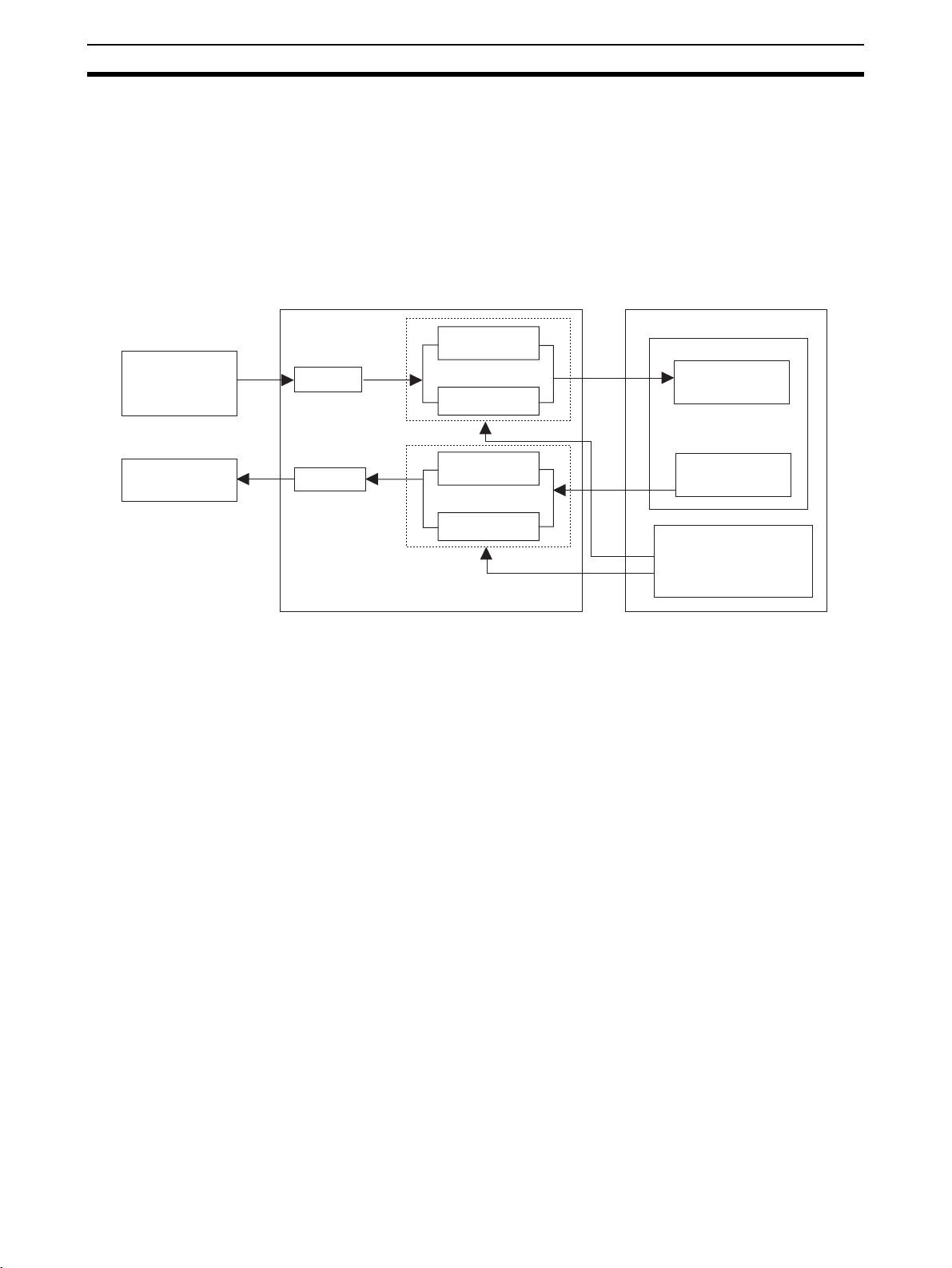
High-speed Conversion The Analog Input Units (CS1W-AD041-V1/081-V1/161 and CJ1W-AD041-V1/
081-V1) and the CJ1W-DA08V/08C Analog Output Unit provide high-speed
data conversion at 250
provides data conversion at 500
µs per I/O point. The CJ1W-MAD42 Analog I/O Unit
µs per I/O point. The sampling period can be
further shortened by setting unused inputs and outputs so that their use is
prohibited.
3
Page 27
Features and Functions Section 1-1
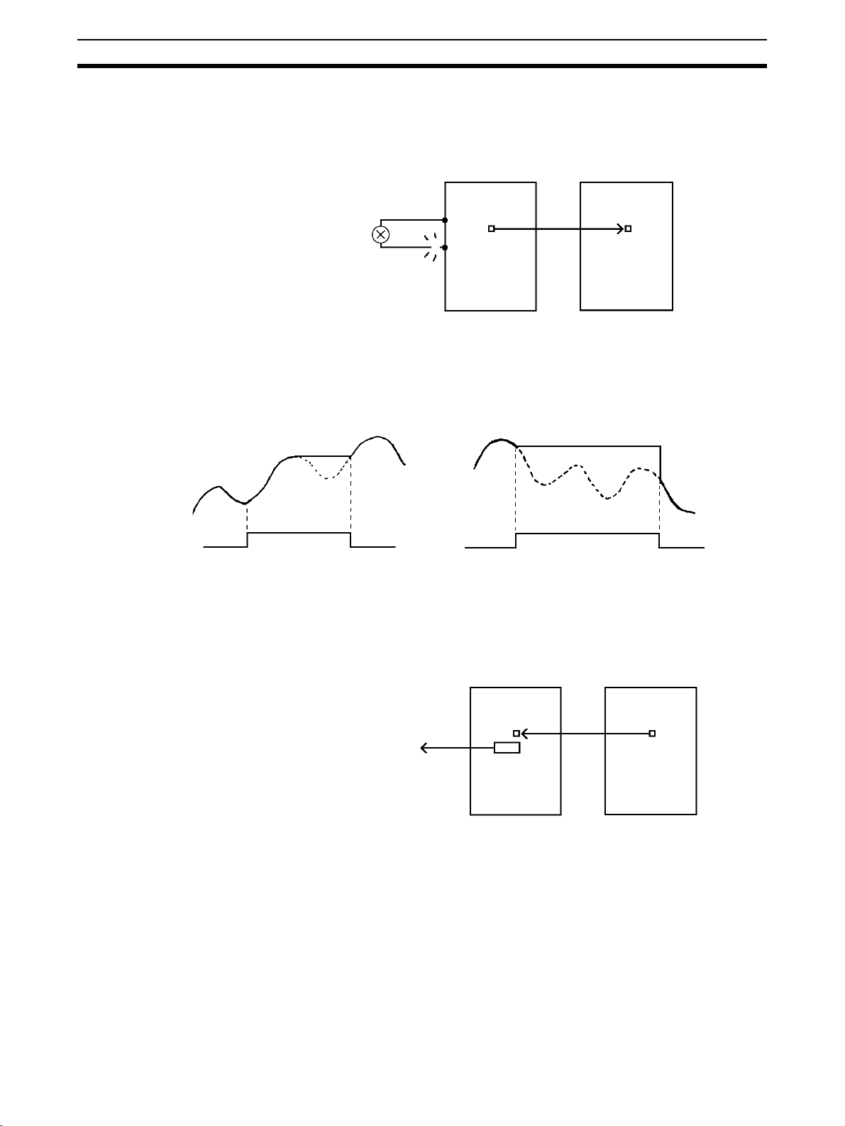
Input Disconnection
Detection Function
The input disconnection detection function can be used for analog inputs
within an input signal range of 1 to 5 V (4 to 20 mA). Any input under 0.3 V will
be regarded as a disconnection. For details, refer to 2-4-3, 2-6-5, or 6-6-4
Input Disconnection Detection Function.
Analog Input Unit CPU Unit
Disconnection
Detection Flag
Peak Value Hold Function The peak value hold function holds the maximum digital conversion value for
every input (including mean value processing). This function can be used with
analog input. The following diagram shows how digital conversion values are
affected when the peak value hold function is used. For details, refer to 2-6-4
or 6-6-3 Peak Value Hold Function.
Peak hold bit
Output Hold Function The output hold function can be used to hold the analog output value at any
preset value when there is a fatal error at the CPU Unit or when specified by
the CPU Unit. When output is stopped, CLR, HOLD, or MAX can be selected
for output. For details, refer to 4-6-3 or 6-7-2 Output Hold Function.
Analog Output Unit CPU Unit
Output Enable
Flag OFF
CLR/HOLD/MAX
4
Page 28
Features and Functions Section 1-1
g
j
Mean Value Function The mean value function can be used to remove erroneous values that occur
due to factors such as noise that is included in analog inputs. The operating
mean is taken without affecting the data refresh cycle. For details, refer to 2-6-
3 or 6-6-2 Mean Value Processing.
Analog Input Unit CPU Unit
Mean value
of "n" history buffers
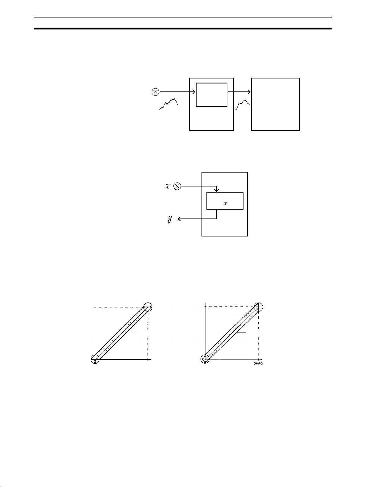
Ratio Conversion
Function
Offset and Gain
Adjustment Function
(Input signal range: 0 to 10 V)
0FA0/(1F40)
The CS1W-MAD44 and CJ1W-MAD42 Analog I/O Unit can output in analog
format the results of analog inputs calculated for ratio and bias. For details,
refer to 6-8 Ratio Conversion Function.
The A/D and D/A converter offset deviation and gain deviation can be
adjusted for each input and output. The offset and gain adjustments are made
with the Unit set for the adjustment mode, and the adjustment values are
stored in the Unit’s built-in EEPROM. For details, refer to 2-7, 4-7 or 6-9
Adjusting Offset and Gain.
Analog Input Function
Adjustable range Adjustable range
Gain
adjustment
Ratio and bias setting device
Analog Output Function
(Output signal range: 0 to 10 V)
10 V
Analog
output
Ratio and biasA x + B
Gain
adjustment
Offset ad
ustment Offset adjustment
Analo
10 V
input
Scaling Function With CS1W-AD161 Analog Input Units, CJ1W-DA08V/08C Analog Output
Units (See note 1.), and CJ1W-MAD42 Analog I/O Units, input analog values
and output analog set values can be automatically converted into user-specified units. This scaling function eliminates the previous need to provide programs (e.g., scaling using the SCL instruction) for numeric conversion to
different units.
When upper and lower limits have been preset in 16-bit binary data in the
CPU Unit’s DM Area, within a decimal range of
−32,000 to +32,000, input
analog values and output analog set values can be automatically converted
5
Page 29
Features and Functions Section 1-1
into user-specified units. (See note 2.) When input values are negative, they
are set using two’s complement.
Note 1. Only output scaling is supported by CJ1W-DA08V/08C Analog Output
Units.
2. This is possible only for a conversion time of 1 ms and a resolution of
4,000. The scaling function is not enabled for a conversion time of 250
(500 µs for the CJ1W-MAD42) and a resolution of 8,000.
Conceptual Diagram of Scaling (CJ1M-MAD42 Only)
µs
Input analog value
(temperature,
flowrate, etc.)
Output analog
value
A/D conversion
D/A conversion
Analog I/O Unit
Power turned ON or
Unit restarted.
No scaling
Scaling
No scaling
Scaling
CPU Unit
Special I/O Unit Area
Converted analog
input value
(in engineering units)
Set analog output
value
(in engineering units)
DM Area
Scaling settings
Input scaling: D(m+27) to
D(m+34)
Output scaling: D(m+19) to
D(m+22)
6
Page 30
Basic Configuration Section 1-2
1-2 Basic Configuration
CS-series PLCs
Temperature
Pressure
Speed
Flow rate
Voltage
Current
Powe r
Power factor
Analog Input Unit
Sensor
Preamp
Transducer
Analog Output Unit
Regulator
Servocontroller
Variable speed
controller
Chart recorder
CPU Unit
(Temperature control)
(Position control)
(Speed control)
Sensor
Note The above diagram is an installation example for the CS1W-AD081-V1 Ana-
log Input Unit and CS1W-DA08V Analog Output Unit.
7
Page 31

Basic Configuration Section 1-2
CJ-series PLCs
CPU Unit
SYSMAC
CJ1G-CPU44
PROGRAMMABLE
CONTROLLER
RUN
ERR/ALM
INH
PRPHL
COMM
OPEN
MCPWR
BUSY
PERIHERAL
AD081
MACH
No.
x10
x10
DA041
RUN
ERC
ERH
ADJ
1
0
B1 A1
RUN
ERC
ERH
ADJ
MACH
No.
1
x10
0
x10
Analog Input Unit
Analog Output Unit
B1 A1
12
PORT
MODE
12
MODE
Sensor
Temperature
Pressure
Speed
Flow rate
Voltage
Current
Power
Power factor
Sensor
Preamp
Transducer
Regulator
Servocontroller
Variable speed
controller
Chart
recorder
(Temperature control)
M
(Position control)
M
(Speed control)
Note The above diagram is an installation example for the CJ1W-AD041-V1/081-V1
Analog Input Unit and CJ1W-DA021/041 Analog Output Unit.
Mounting Restrictions
CS-series PLCs The CS1W-MAD44 Analog I/O Unit is a Special I/O Unit of the CS Series.
CS1W-MAD44 Analog I/O Units can be mounted to either CS-series CPU
Racks or CS-series Expansion Racks. These Analog I/O Units cannot be
mounted to C200H Expansion I/O Racks or SYSMAC BUS Slave Racks.
The number of Analog I/O Units that can be mounted to one Rack (i.e., a CPU
Rack or Expansion Rack) depends on the maximum supply current of the
Power Supply Unit and the current consumption of other Units. If a Rack is to
be mounted with Analog Input, Output, or I/O Units only, the following restrictions will apply.
Power Supply Unit Rack CS1W-
AD041-V1
CS1W-
AD081-V1
(5 VDC
120 mA)
C200HW-PA204
C200HW-PA204S
C200HW-PA204R
CPU Rack63328
Expansion Rack63329
C200HW-PA204C
C200HW-PD024
(4.6 A at 5 VDC)
C200HW-PA209R
(9 A at 5 VDC)
CS1D-PA207R
(7 A at 5 VDC)
CS1D-PD024
(4.3 A at 5 VDC)
CPU Rack1076510
Expansion Rack1076510
CPU Rack85448
Expansion Rack96549
CPU Rack63227
Expansion Rack63228
8
CS1W-DA041
CS1W-DA08V
(5 VDC
130 mA)
CS1WMAD44
(5 VDC
200 mA)
CS1W-DA08C
(5 VDC
130 mA)
CS1W-AD161
(5 VDC
150 mA)
Page 32

Basic Configuration Section 1-2
Note The I/O bits of the Special I/O Unit are allocated according to the setting of the
unit number switch on the front panel of the Unit, and not the slot number
where the Unit is mounted.
CJ-series PLCs CJ-series Analog I/O Units are Special I/O Unit of the CJ-series PLCs.
These Units can be connected in the CJ-series CPU Rack or Expansion
Racks. The number of Analog I/O Units that can be connected in each Rack
will depend on the current consumption of the other Units in the Rack. The following table shows the maximum number of Analog I/O Units that can be connected in one Rack if no other I/O Units are connected.
Power Supply Unit Rack CJ1W-DA021
CJ1W-DA041
(5 VDC 120 mA)
CJ1W-DA08V
CJ1W-DA08C
(5 VDC 140 mA)
CJ1W-PA205R
CJ1W-PA205C
CJ1W-PD025
(5.0 A at 5 VDC)
CJ1W-PA202
(2.8 A at 5 VDC)
CJ1W-PD022
(2.0 A at 5 VDC)
CPU Rack 10 9 7
Expansion Rack 10 10 8
CPU Rack 10 4 3
Expansion Rack 10 6 4
CPU Rack 7 2 1
Expansion Rack 10 4 3
Note The I/O bits of the Special I/O Unit are allocated according to the setting of the
unit number switch on the front panel of the Unit, and not the order in which it
is connected.
1-2-1 Mounting Procedure
CS-series PLCs
Use the following procedure to mount Analog I/O Units to the Backplane.
1,2,3... 1. Lock the top of the Analog I/O Unit into the slot on the Backplane and rotate
the Unit downwards as shown in the following diagram.
CS1W-AD041-V1
CJ1W-AD081-V1
(5 VDC 420 mA)
CJ1W-MAD42
(5 VDC 580 mA)
Hook
Backplane
2. While making sure to align the Unit properly with the connectors, tighten
the mounting screws securely to the tightening torque of 0.4 N·m.
9
Page 33

Basic Configuration Section 1-2
3. To remove the Unit, first loosen the mounting screws using a Phillips
screwdriver.
Mounting screw
Leave enough space below each Rack, as shown in the following diagram for
mounting and removing the Units.
20 mm min.
Backplane
CJ-series PLCs
20 mm min.
Phillips screwdriver
Analog I/O Units are connected as I/O Units in the system configuration, as
shown below.
CPU Rack
SYSMAC
CJ1G-CPU44
PROGRAMMABLE
CONTROLLER
MCPWR
BUSY
OPEN
ERR/ALM
PERIHERAL
PORT
RUN
INH
PRPHL
COMM
AD081
MACH
No.
x
x
RUN
ERC
ERH
ADJ
1
10
0
10
12
MODE
Power Supply Unit CPU Unit I/O Units (10 max.)
DA041
RUN
ERC
B1 A1
ERH
B1 A1
ADJ
MACH
No.
1
x
10
0
x
10
12
MODE
End Cover
(included with CPU Unit)
10
Use the following procedure to connect Analog I/O Units to a CJ-series Rack.
Page 34

Basic Configuration Section 1-2
1,2,3... 1. Align the connectors and press in firmly on the Units to connect them com-
pletely.
Hooks
Connector
2. Move the sliders on the top and bottom of the Unit to the lock position to
secure the Units. The sliders should click into place.
Move the sliders to the back
until they click into place.
Hook holes
Note The CJ-series PLC may not operate properly if the sliders are not locked
1-2-2 Precautions
Lock
Slider
Release
3. Attach an End Cover to the Unit on the right end of the Rack.
firmly into place.
Be sure to turn OFF the power supply to the PLC before installing or disconnecting Units or connecting lines.
To reduce the risk of malfunctioning due to electrical noise, wire input and output lines in separate ducts from high-voltage and power lines.
When wiring a Unit, place a label over the top of the Unit to prevent wire clippings or other materials from getting inside the Unit. When the wiring has
been completed, the label must be removed to prevent heat radiation.
CS-series PLCs
Remove the label after the
wiring has been completed.
11
Page 35

Function Applications Section 1-3
CJ-series PLCs
Remove the label after the
wiring has been completed.
AD081
AD081
UN
UN
R
R
RC
RC
E
E
RH
RH
E
E
DJ
DJ
A
A
H
H
C
C
A
A
M
M
.
.
1
1
No
No
0
0
1
1
x
x
0
0
0
0
1
1
x
x
12
12
E
E
OD
OD
M
M
1-3 Function Applications
Function Application Page
Mean value processing Performs a smooth conversion when the input fluctuation is too extreme.
Example: Removes noise interference from data such as flow/pressure.
Peak value hold Holds the maximum value that has been read.
Holds the data that is less than the maximum value.
Disconnection detection Detects disconnection of input signals. 59, 258
Output hold Holds the output signal at the previous value for certain conditions, such as
errors.
Holds the output signal in the lower-limit value or 0 V for certain conditions,
such as errors.
Holds the output signal in the upper-limit value for certain conditions, such
as errors.
Ratio conversion Uses the Analog I/O Unit as a gradient setting device for setting ratio and
bias.
Offset gain adjustment Adjusts the offset and gain, and uses the I/O functions. 60, 153, 265
55, 254
58, 257
152, 261
262
12
Page 36

CS-series Analog Input Units
This section explains how to use the CS1W-AD041-V1/081-V1/161 Analog Input Units.
2-1 Specifications . . . . . . . . . . . . . . . . . . . . . . . . . . . . . . . . . . . . . . . . . . . . . . . . . 14
2-1-1 Specifications . . . . . . . . . . . . . . . . . . . . . . . . . . . . . . . . . . . . . . . . . . 14
2-1-2 Input Function Block Diagram . . . . . . . . . . . . . . . . . . . . . . . . . . . . . 17
2-1-3 Input Specifications . . . . . . . . . . . . . . . . . . . . . . . . . . . . . . . . . . . . . 17
2-2 Operating Procedure . . . . . . . . . . . . . . . . . . . . . . . . . . . . . . . . . . . . . . . . . . . . 20
2-2-1 Procedure Examples . . . . . . . . . . . . . . . . . . . . . . . . . . . . . . . . . . . . . 21
2-3 Components and Switch Settings . . . . . . . . . . . . . . . . . . . . . . . . . . . . . . . . . . 27
2-3-1 Indicators . . . . . . . . . . . . . . . . . . . . . . . . . . . . . . . . . . . . . . . . . . . . . 28
2-3-2 Unit Number Switch . . . . . . . . . . . . . . . . . . . . . . . . . . . . . . . . . . . . . 29
2-3-3 Operation Mode Switch . . . . . . . . . . . . . . . . . . . . . . . . . . . . . . . . . . 30
2-3-4 Voltage/Current Switch (CS1W-AD041-V1/AD081-V1) . . . . . . . . 31
2-4 Wiring . . . . . . . . . . . . . . . . . . . . . . . . . . . . . . . . . . . . . . . . . . . . . . . . . . . . . . . 32
2-4-1 Terminal Arrangement . . . . . . . . . . . . . . . . . . . . . . . . . . . . . . . . . . . 32
2-4-2 Internal Circuitry . . . . . . . . . . . . . . . . . . . . . . . . . . . . . . . . . . . . . . . 33
2-4-3 Voltage Input Disconnection. . . . . . . . . . . . . . . . . . . . . . . . . . . . . . . 35
2-4-4 Input Wiring Example . . . . . . . . . . . . . . . . . . . . . . . . . . . . . . . . . . . 36
2-4-5 Input Wiring Considerations. . . . . . . . . . . . . . . . . . . . . . . . . . . . . . . 38
2-5 Exchanging Data with the CPU Unit . . . . . . . . . . . . . . . . . . . . . . . . . . . . . . . 39
2-5-1 Outline of Data Exchange. . . . . . . . . . . . . . . . . . . . . . . . . . . . . . . . . 39
2-5-2 Unit Number Settings . . . . . . . . . . . . . . . . . . . . . . . . . . . . . . . . . . . . 40
2-5-3 Special I/O Unit Restart Bits . . . . . . . . . . . . . . . . . . . . . . . . . . . . . . 41
2-5-4 Fixed Data Allocations . . . . . . . . . . . . . . . . . . . . . . . . . . . . . . . . . . . 41
2-5-5 I/O Refresh Data Allocations . . . . . . . . . . . . . . . . . . . . . . . . . . . . . . 46
2-6 Analog Input Functions and Operating Procedures . . . . . . . . . . . . . . . . . . . . 52
2-6-1 Input Settings and Conversion Values . . . . . . . . . . . . . . . . . . . . . . . 52
2-6-2 Conversion Time/Resolution Setting . . . . . . . . . . . . . . . . . . . . . . . . 54
2-6-3 Mean Value Processing. . . . . . . . . . . . . . . . . . . . . . . . . . . . . . . . . . . 55
2-6-4 Peak Value Hold Function . . . . . . . . . . . . . . . . . . . . . . . . . . . . . . . . 58
2-6-5 Input Disconnection Detection Function . . . . . . . . . . . . . . . . . . . . . 59
2-6-6 Scaling Function (CS1W-AD161 Only) . . . . . . . . . . . . . . . . . . . . . . 60
2-7 Adjusting Offset and Gain . . . . . . . . . . . . . . . . . . . . . . . . . . . . . . . . . . . . . . . 60
2-7-1 Adjustment Mode Operational Flow . . . . . . . . . . . . . . . . . . . . . . . . 60
2-7-2 Input Offset and Gain Adjustment Procedures. . . . . . . . . . . . . . . . . 62
2-8 Handling Errors and Alarms . . . . . . . . . . . . . . . . . . . . . . . . . . . . . . . . . . . . . . 69
2-8-1 Indicators and Error Flowchart. . . . . . . . . . . . . . . . . . . . . . . . . . . . . 69
2-8-2 Alarms Occurring at the Analog Input Unit . . . . . . . . . . . . . . . . . . . 70
2-8-3 Errors in the CPU Unit . . . . . . . . . . . . . . . . . . . . . . . . . . . . . . . . . . . 73
2-8-4 Restarting Special I/O Units . . . . . . . . . . . . . . . . . . . . . . . . . . . . . . . 74
2-8-5 Troubleshooting . . . . . . . . . . . . . . . . . . . . . . . . . . . . . . . . . . . . . . . . 74
SECTION 2
13
Page 37

Specifications Section 2-1
2-1 Specifications
2-1-1 Specifications
Item CS1W-AD041-V1 CS1W-AD081-V1 CS1W-AD161
Unit type CS-series Special I/O Unit
Isolation (See note 1.) Between I/O and PLC signals: Photocoupler
External terminals 21-point detachable terminal block (M3 screws) Two 34-pin MIL connectors
Affect on CPU Unit cycle time 0.2 ms
Power consumption 120 mA max. at 5 VDC, 90 mA max. at 26 VDC 150 mA max. at 5 VDC,
Dimensions (mm) (See note 2.) 35 x 130 x 126 (W x H x D) 35 x 130 x 119 (W x H x D)
Weight 450 g max.
General specifications Conforms to general specifications for SYSMAC CS Series.
Mounting position CS-series CPU Rack or CS-series Expansion Rack
Maximum number of Units
(See note 3.)
Data exchange with CPU Units
(See note 4.)
Input
specifications
Number of analog inputs 4 8 16
Input signal range
(See note 5.)
Maximum rated input (for
1 point) (See note 7.)
Input impedance Voltage Input: 1 MΩ min.
Resolution 4,000/8,000 (See note 8.)
Converted output data 16-bit binary data
Accuracy
(See note
9.)
A/D conversion time
(See note 10.)
23±2°C Voltage Input: ±0.2% of full scale
0°C to 55°C Voltage Input:±0.4% of full scale
(No isolation between individual I/O signals.)
55 mA max. at 26 VDC
(Cannot be mounted to a C200H Expansion I/O Rack or a SYSMAC BUS Slave
Rack.)
Refer to the table on page 15.
Special I/O Unit Area in CIO Area (CIO 2000 to CIO
2959): 10 words per Unit
Special I/O Unit Area in DM Area (D20000 to D29599):
100 words per Unit
1 to 5 V
0 to 5 V
0 to 10 V
–10 to 10 V
4 to 20 mA
(See note 6.)
Voltage Input: ±15 V
Current Input: ±30 mA
Current Input: 250 Ω (rated value)
Current Input: ±0.4% of full scale
Current Input: ±0.6% of full scale
1.0 ms or 250 µs per point max. (See note 8.)
Special I/O Unit Area in
CIO Area (CIO 2000 to
CIO 2959): 20 words per
Unit
Special I/O Unit Area in
DM Area (D20000 to
D29599): 200 words per
Unit
Voltage Input: ±0.2% of full
scale
Current Input: ±0.2% of full
scale
Voltage Input:±0.4% of full
scale
Current Input: ±0.4% of full
scale
14
Page 38

Specifications Section 2-1
Item CS1W-AD041-V1 CS1W-AD081-V1 CS1W-AD161
Input
functions
Mean value processing Stores the last “n” data conversions in the buffer, and stores the mean value of the
Peak value holding Stores the maximum conversion value while the Peak Value Hold Bit is ON.
Input disconnection
detection
Scaling function None None Enabled only for conver-
conversion values.
Buffer number: n = 2, 4, 8, 16, 32, 64
Detects the disconnection and turns ON the Disconnection Detection Flag. (See note
11.)
sion time of 1 ms and resolution of 4,000. Setting any
values within a range of
±32,000 as the upper and
lower limits allows the A/D
conversion result to be output with these values as
full scale.
Note 1. Do not apply a voltage higher than 600 V to the terminal block when per-
forming withstand voltage test on this Unit. Otherwise, internal elements
may deteriorate.
2. Refer to Dimensions on page 359 for details on the Unit’s dimensions.
3. The maximum number of Analog Input Units that can be mounted to one
Rack depends on the Power Supply Unit mounted to the Rack.
Power Supply Unit Rack CS1W-
AD041-V1
CS1W-
AD081-V1
(5 VDC
120 mA)
C200HW-PA204
C200HW-PA204S
C200HW-PA204R
C200HW-PA204C
C200HW-PD024
(4.6 A at 5 VDC)
C200HW-PA209R
(9 A at 5 VDC)
CS1D-PA207R
(7 A at 5 VDC)
CS1D-PD024
(4.3 A at 5 VDC)
CPU Rack63328
Expansion Rack63329
CPU Rack1076510
Expansion Rack1076510
CPU Rack85448
Expansion Rack96549
CPU Rack63227
Expansion Rack63228
The above limits may be reduced depending on the power consumed by
other Units on the same Rack.
CS1W-DA041
CS1W-DA08V
(5 VDC
130 mA)
CS1WMAD44
(5 VDC
200 mA)
CS1W-DA08C
(5 VDC
130 mA)
CS1W-AD161
(5 VDC
150 mA)
15
Page 39

Specifications Section 2-1
4. Data Exchange with the CPU Unit
Area Number of words Data transfer
Special I/O Unit Area
in CIO Area
(CIO 2000 to
CIO 2959,
CIO 2000.00 to
CIO 2959.15)
Special I/O Unit Area
in DM Area
(D20000 to D26959)
• CS1W-AD041-V1/
081-V1: 10 words per
Unit
• CS1W-AD161: 20
words per Unit
• CS1W-AD041-V1/
081-V1: 100 words
per Unit
• CS1W-AD161: 200
words per Unit
Note The resolution/conversion time setting and operation mode setting
5. Input signal ranges can be set for each input.
6. Voltage input or current input is selected for the CS1W-AD041-V1 and
CS1W-AD081-V1 by using the voltage/current switch at the back of the terminal block. Voltage input or current input is selected for the CS1W-AD161
by wiring the connector terminals. Voltage/current selection for input ranges 1 to 5 V or 4 to 20 mA can be set in DM word m+52.
7. Use the analog input voltage/current value within the specified input signal
range. Exceeding the specified range may result in malfunction.
8. With Analog Input Units, the resolution can be changed from 4,000 to
8,000 and the conversion time changed from 1 ms to 250
m+18 for CS1W-AD041-V1 and CS1W-AD081-V1 or in DM word m+19 for
CS1W-AD161.
9. The following are adjusted at the factory.
CS1W-AD041-V1/081-V1: Voltage inputs
CS1W-AD161: Voltage inputs and current inputs
To use current inputs with the CS1W-AD041-V1/081-V1 or to use the
CS1W-AD161 with products other than the recommended ones, adjust the
offset and gain as required.
10. A/D conversion time is the time it takes for an analog signal to be stored in
memory as converted data after it has been input. It takes at least one cycle before the converted data is read by the CPU Unit.
11. Input disconnection detection is valid only when the 1 to 5-V or 4 to 20-mA
range is set. If there is no input signal for when the 1 to 5-V or 4 to 20-mA
range is set, the Disconnection Detection Flag will turn ON.
Transfer direction Data contents
timing
Constantly CPU Unit to Ana-
When power is
turned ON or
Unit is
restarted
log Input Unit
Analog Input Unit
to CPU Unit
CPU Unit to Analog Input Unit
Peak hold indicators
Analog input values
Line disconnection detection
Alarm flags
Etc.
Input signal conversion ON/OFF
Signal range specifications
Averaging specifications
Resolution/conversion time setting
Operation mode setting
Scaling setting (CS1W-AD161 only)
are supported only by version-1 Analog Input Units.
Calibration conditions: Recommended Terminal BlockConnector Conversion Unit used. (The factory calibration
for a current input can be made effective by setting DM
word m+52.)
µs in DM word
16
Page 40

Specifications Section 2-1
g
2-1-2 Input Function Block Diagram
Analog Input Unit CPU Unit
Analog input 1
Analog input 2
Analog input 3
Analog input 4
Analog input 5
Analog input 6
Analog input 7
Analog input 8
A/D
Same as above.
Same as above.
Same as above.
Same as above. (See note.)
Same as above. (See note.)
Same as above. (See note.)
Same as above. (See note.)
Input disconnection
detection
Note There are only four analog inputs for the CS1W-AD041-V1, and 16 analog
inputs for the CS1W-AD161.
2-1-3 Input Specifications
If signals that are outside the specified range provided below are input, the
conversion values (16-bit binary data) used will be either the maximum or
minimum value.
Mean value
processing
disabled
Mean value
processing
enabled
Peak value
hold function
disabled
Peak value
hold function
enabled
I/O
refresh
Special I/O
Unit Area
Analog
input 1
conversion
value
Range: 1 to 5 V (4 to 20 mA)
Conversion value
1068 (20D0)
0FA0 (1F40)
0000 (0000)
FF38 (FE70)
1 V/4 mA
0.8 V/3.2 mA
5 V/20 mA
5.2 V/20.8 mA
input signal
Analo
Resolution: 4,000
(Resolution: 8,000)
17
Page 41

Specifications Section 2-1
g
Range: 0 to 10 V
Conversion value
1068 (20D0)
0FA0 (1F40)
Resolution: 4,000
(Resolution: 8,000)
0000 (0000)
FF38 (FE70)
0 V 10 V
–0.5 V 10.5 V
input signal
Analo
Range: 0 to 5 V
Conversion value
1068 (20D0)
0FA0 (1F40)
0000 (0000)
FF38 (FE70)
Resolution: 4,000
(Resolution: 8,000)
0 V 5 V
–0.25 V 5.25 V
Analog input signal
18
Page 42

Specifications Section 2-1
g
Range: –10 to 10 V
Conversion value
0898 (1130)
07D0 (0FA0)
Resolution: 4,000
0000 (0000)
F830 (F060)
F768 (EED0)
(Resolution: 8,000)
–10 V
–11 V
0 V 10 V
Analo
11 V
input signal
Note The conversion values for a range of –10 to 10 V will be as follows (for a reso-
lution of 4,000):
16-bit binary data BCD
F768 –2200
::
FFFF –1
0000 0
0001 1
::
0898 2200
19
Page 43

Operating Procedure Section 2-2
2-2 Operating Procedure
Follow the procedure outlined below when using Analog Input Units.
Installation and Settings
1,2,3... 1. Set the operation mode to normal mode. (See note 1.)
2. Select voltage/current input using the switch at the back of the terminal
block. (See note 2.)
3. Wire the Unit.
4. Use the unit number switch on the front panel of the Unit to set the unit
number. (See note 3.)
5. Turn ON the power to the PLC.
6. Create the Input tables.
7. Make the Special Input Unit DM Area settings.
• Set the input numbers to be used.
• Set the input signal ranges.
• Set the number of mean processing samplings.
• Conversion time and resolution
8. Turn the power to the PLC OFF and ON, or turn ON the Special I/O Unit
Restart Bit to ON.
When the input for the connected devices needs to be calibrated, follow the
procedures in Offset Gain Adjustment below. Otherwise, skip to Operation
below.
Offset and Gain Adjustment
Operation
1,2,3... 1. Set the operation mode to adjustment mode. (See note 1.)
2. Select voltage or current input. (See note 2.)
3. Turn ON the power to the PLC.
4. Adjust the offset and gain.
5. Turn OFF the power to the PLC.
6. Set the operation mode to normal mode. (See note 1.)
1,2,3... 1. Turn ON the power to the PLC.
2. Ladder program
• Read conversion values or write set values by means of MOV(021)
and XFER(070).
• Specify the peak hold function.
• Obtain disconnection notifications and error codes.
Note 1. Setting the Operation Mode
The operation mode can be changed either by setting the DIP switch on
the rear panel of the Unit or changing the DM Area settings. When normal
mode is set both in the DIP switch and in the DM Area settings, the Unit
operates in normal mode. If adjustment mode is set in either or both of the
settings, the Unit operates in adjustment mode. The operation mode selection setting is allocated in DM word m+18 for CS1W-AD041-V1 and CS1WAD081-V1 and in DM word m+19 for CS1W-AD161.
2. Selecting Voltage/Current Input
With the CS1W-AD041-V1 and CS1W-AD081-V1, remove the terminal
block and set the DIP switch located at the back. With the CS1W-AD161,
20
Page 44

Operating Procedure Section 2-2
select either voltage input or current input by wiring the connector terminals. Use DM word m+52 to select 1 to 5 V or 4 to 20 mA as the voltage or
current input range, respectively.
3. Setting the Unit Number
Set the unit number for the Special I/O Unit using the rotary switches on
the front panel of the Unit.
Set the CS1W-AD041-V1 and CS1W-AD081-V1 between 0 and 95. A single CS1W-AD161 is allocated words in the CIO Area and DM Area for two
Units. Set the unit number between 0 and 94. To set a CS1W-AD161 to unit
number "n," the unit number setting "n+1" is not possible.
2-2-1 Procedure Examples
The procedure for using Analog Input Units is provided here using the CS1WAD081-V1 as an example. The method used to set CS1W-AD161 Analog
Input Units is different. Be sure to use the correct procedure.
CS1W-AD081-V1 CS-series CPU Unit
IN1: 1 to 5 V
IN2: 1 to 5 V
IN3: 4 to 20 mA
Analog input
IN4: 4 to 20 mA
IN5: 0 to 10 V
IN6: 0 to 10 V
IN7: –10 to 10 V
IN8: Not used
Ladder Program
Setting the Analog Input Unit
1,2,3... 1. Set the operation mode. Refer to 2-3-3 Operation Mode Switch for further
Unit No.: 1
details.
Turn OFF SW1 for normal mode
The operation mode can be changed by setting DM word m+18 (DM word
m+19 for CS1W-AD161).
21
Page 45

Operating Procedure Section 2-2
2. Set the voltage/current switch. Refer to 2-3-4 Voltage/Current Switch
(CS1W-AD041-V1/AD081-V1) for further details.
Pins IN1 to IN8 correspond to analog inputs 1 to 8.
E.g., To use voltage input for analog inputs 1 and 2,
turn OFF IN1 and IN2.
To use current input for analog inputs 3 and 4, turn
ON IN3 and IN4.
Note With CS1W-AD161, select voltage/current input by wiring the connector termi-
nals.
3. Mount and wire the Analog Input Unit. Refer to 1-2-1 Mounting Procedure,
2-4 Wiring or 2-4-4 Input Wiring Example for further details.
4. Set the unit number switch. Refer to 2-3-2 Unit Number Switch for further
details.
22
Page 46

Operating Procedure Section 2-2
If the unit number is set to 1, words will be allocated to the Special I/O Unit
Area CIO 2010 to CIO 2019 and to the Special I/O Unit Area D20100 to
D20199.
Note A single CS1W-AD161 is allocated CIO Area words and DM Area words for
two Units. For example, if the unit number is set to 1, the CS1W-AD161 will be
allocated CIO Area words CIO 2010 to CIO 2029 and DM Area words D20100
to D20299.
5. Turn ON the power to the PLC.
Powe r O N
Creating I/O Tables
After turning ON the power to the PLC, be sure to create the I/O tables.
Peripheral port
23
Page 47

Operating Procedure Section 2-2
Initial Data Settings
1,2,3... 1. Specify the Special I/O Unit DM Area settings. Refer to 2-5-4 Fixed Data
Allocations for further details.
Peripheral port
Setting conditions
Unit No. 1
Analog input 1: 1 to 5 V
Analog input 2: 1 to 5 V
Analog input 3: 4 to 20 mA
Analog input 4: 4 to 20 mA
Analog input 5: 0 to 10 V
Analog input 6: 0 to 10 V
Analog input 7: –10 to 10 V
Analog input 8: Not used.
• The following diagram shows the input settings used. Refer to DM Allocation Contents on page 41 and 2-6-1 Input Settings and Conversion
Val ues for more details.
Bit
m: D20100
(007F Hex)
• The following diagram shows the input range settings. Refer to DM Al-
location Contents on page 41 and 2-6-1 Input Settings and Conversion
Val ues for more details.
Input 1: 1 to 5 V. Set to 10.
Input 2: 1 to 5 V. Set to 10.
Input 3: 4 to 20 mA. Set to 10.
Input 4: 4 to 20 mA. Set to 10.
15 14 13 12 11 10 09 08 07 06 05 01 0004 03 02
Bit
15 14 13 12 11 10 09 08 07 06 05 01 0004 03 02
0 0 0 0 0 0 0 0 0 1 1 1 1 1 1 1
Not used
Used
Input 8
Input 7
Input 6
Input 5
Input 4
Input 3
Input 2
Input 1
24
m+1: D20101
(05AA Hex)
0 0 0 0 0 1 0 1 1 0 1 0 1 0 1 0
Input 5: 0 to 10 V. Set to 01.
Input 6: 0 to 10 V. Set to 01.
Input 7: −10 to 10 V. Set to 00.
Input 8: Not used. Set to 00 (disabled)
Also set DM word m+52 when using current input with the CS1W-AD161.
Page 48

Operating Procedure Section 2-2
• The following diagram shows the conversion time/resolution setting.
m+18: D20118
(See note.)
(0000 Hex)
Note For CS1W-AD161, set D(m+19):D20119.
(Refer to
15 14 13 12 11 10 09 08 07 06 05 01 0004 03 02
Bit
0 0 0 0 0 0 0 0
2. Restart the CPU Unit.
2-6-2 Conversion Time/Resolution Setting.)
Conversion Time/Resolution Setting
0000: 1-ms conversion time, 4,000 resolution
C100: 250-
µs conversion time, 8,000 resolution
Power turned ON again
(or Special I/O Unit Restart Bit is turned ON)
Creating Ladder Programs
Peripheral port
The data that is converted from analog to digital and output to CIO words (n +
1) to (n+ 7) of the Special I/O Unit Area (CIO 2011 to CIO2017), is stored in
the specified addresses D00100 to D00106 as signed binary values 0000 to
0FA0 Hex.
25
Page 49

Operating Procedure Section 2-2
• The following table shows the addresses used for analog input.
Input number Input signal range Input conversion
value address
(n = CIO 2010)
(See note 1.)
1 1 to 5 V (n+1) = CIO 2011 D00100
2 1 to 5 V (n+2) = CIO 2012 D00101
3 4 to 20 mA (n+3) = CIO 2013 D00102
4 4 to 20 mA (n+4) = CIO 2014 D00103
5 0 to 10 V (n+5) = CIO2015 D00104
6 0 to 10 V (n+6) = CIO2016 D00105
7 –10 to 10 V (n+7) = CIO2017 D00106
8 Not used --- ---
Note 1. The addresses are fixed according to the unit number of the Special I/O
Unit. Refer to 2-3-2 Unit Number Switch for further details.
2. Set as required.
Conversion data
holding address
(See note 2.)
201900 Input 1 Disconnection Detection Flag (See note 3.)
201901 Input 2 Disconnection Detection Flag (See note 3.)
201902 Input 3 Disconnection Detection Flag (See note 3.)
201903 Input 4 Disconnection Detection Flag (See note 3.)
3. The input Disconnection Detection Flag is allocated to bits 00 to 07 of word
(n + 9). Refer to Allocations for Normal Mode on page 47 for further details.
MOV (021)
MOV (021)
MOV (021)
MOV (021)
2011
D00100
2012
D00101
2013
D00102
2014
D00103
For 1 to 5 V, the hexadecimal value 0000
to 0FA0 will be stored in CIO 2011, so if
there is no disconnection (i.e., 201900 is
OFF), CIO 2011 will be stored in
D00100.
In the same way, for 1 to 5 V, CIO 2012
will be stored in D00101.
In the same way, for 4 to 20 mA, CIO 2013
will be stored in D00102.
In the same way, for 4 to 20 mA, CIO 2014
will be stored in D00103.
26
Page 50

Components and Switch Settings Section 2-3
2-3 Components and Switch Settings
CS1W-AD041-V1 CS1W-AD081-V1
Front
With Terminal Block With Terminal Block Removed
With Terminal Block With Terminal Block Removed
Front
Unit number
setting switch
External
terminal block
mounting
screws
(black M3)
External
terminal
block (M3)
Operation mode switch
Back
Voltage/
Current
switch
Terminal block
Unit number
setting switch
External
terminal block
mounting
screws
(black M3)
External
terminal
block (M3)
Side
Voltage/
Current
switch
Backplane connector
27
Page 51

Components and Switch Settings Section 2-3
r
The terminal block is attached by a connector. It can be removed by loosening
the two black mounting screws located at the top and bottom of the terminal
block.
Check to be sure that the black terminal block mounting screw is securely
tightened to a torque of 0.5 N·m.
Fasten the mounting screw.
CS1W-AD161
34.5
130
Input connector 2
(Inputs 9 to 16)
2-3-1 Indicators
Input connector 1
(Inputs 1 to 8)
118.03
100.5
Backplane mounting screw
Fasten the mounting
Mode Switch
(two poles)
PC21 bus connecto
screw.
28
The indicators show the operating status of the Unit. The following table
shows the meanings of the indicators.
LED Meaning Indicator Operating status
RUN (green) Operating Lit Operating in normal mode.
Not lit Unit has stopped exchanging data with
the CPU Unit.
ERC (red) Error
detected by
Unit
Lit Alarm has occurred (such as disconnec-
tion detection) or initial settings are incorrect.
Not lit Operating normally.
Page 52

Components and Switch Settings Section 2-3
LED Meaning Indicator Operating status
ADJ (yellow) Adjusting Flashing Operating in offset/gain adjustment
Not lit Other than the above.
ERH (red) Error in the
CPU Unit
Lit Error has occurred during data exchange
Not lit Operating normally.
mode.
with the CPU Unit.
2-3-2 Unit Number Switch
The CPU Unit and Analog Input Unit exchange data via the Special I/O Unit
Area and the Special I/O Unit DM Area. The Special I/O Unit Area and Special
I/O Unit DM Area word addresses that each Analog Input Unit occupies are
set by the unit number switch on the front panel of the Unit.
Always turn OFF the power before setting the unit number. Use a flat-blade
screwdriver, being careful not to damage the slot in the screw. Be sure not to
leave the switch midway between settings.
Switch
setting
0 Unit #0 CIO 2000 to
1 Unit #1 CIO 2010 to
2 Unit #2 CIO 2020 to
3 Unit #3 CIO 2030 to
4 Unit #4 CIO 2040 to
5 Unit #5 CIO 2050 to
6 Unit #6 CIO 2060 to
7 Unit #7 CIO 2070 to
8 Unit #8 CIO 2080 to
9 Unit #9 CIO 2090 to
10 Unit #10 CIO 2100 to
~~ ~ ~ ~ ~ ~
n Unit #n CIO 2000 + (n x 10)
~~ ~ ~ ~ ~ ~
94 Unit #94 CIO 2940 to
95 Unit #95 CIO 2950 to
Unit
number
CS1W-AD041-V1/AD081-V1 CS1W-AD161 (See note 2.)
Special/O Unit Area
addresses
CIO 2009
CIO 2019
CIO 2029
CIO 2039
CIO 2049
CIO 2059
CIO 2069
CIO 2079
CIO 2089
CIO 2099
CIO 2109
to CIO 2000 + (n x
10) + 9
CIO 2949
CIO 2959
Special I/O Unit DM
Area addresses
D20000 to D20099 Unit #0 CIO 2000 to
D20100 to D20199 Unit #1 CIO 2010 to
D20200 to D20299 Unit #2 CIO 2020 to
D20300 to D20399 Unit #3 CIO 2030 to
D20400 to D20499 Unit #4 CIO 2040 to
D20500 to D20599 Unit #5 CIO 2050 to
D20600 to D20699 Unit #6 CIO 2060 to
D20700 to D20799 Unit #7 CIO 2070 to
D20800 to D20899 Unit #8 CIO 2080 to
D20900 to D20999 Unit #9 CIO 2090 to
D21000 to D21099 Unit #10 CIO 2100 to
D20000 + (n x 100)
to
D20000 + (n x 100) +
99
D29400 to D29499 Unit #94 CIO 2940 to
D29500 to D29599 Not
Unit
number
Unit #n CIO 2000 + (n x 10)
used.
Special/O Unit Area
addresses
CIO 2019
CIO 2029
CIO 2039
CIO 2049
CIO 2059
CIO 2069
CIO 2079
CIO 2089
CIO 2099
CIO 2109
CIO 2119
to CIO 2000 + (n x
10) + 19
CIO 2959
--- ---
Special I/O Unit DM
D20000 to D20199
D20100 to D20299
D20200 to D20399
D20300 to D20499
D20400 to D20599
D20500 to D20699
D20600 to D20799
D20700 to D20899
D20800 to D20999
D20900 to D21099
D21000 to D21199
D20000 + (n x 100)
to
D20000 + (n x 100) +
199
D29400 to D29499
Area addresses
29
Page 53

Components and Switch Settings Section 2-3
Note 1. If two or more Special I/O Units are assigned the same unit number, a
“UNIT No. DPL ERR” error (in the Programming Console) will be generated (A40113 will turn ON) and the PLC will not operate.
2. A single CS1W-AD161 is allocated CIO Area words and DM Area words
for two Units. Be sure to set a unit number so that the CS1W-AD161 is not
allocated words in the CIO Area and DM Area that are already allocated to
other Special I/O Units. For example, if the CS1W-AD161 is set to unit
number n, another Special I/O Unit cannot be set with unit number n+1.
The highest unit number that can be set for a CS1W-AD161 is unit number
94.
2-3-3 Operation Mode Switch
The operation mode switch on the back panel of the Unit is used to set the
operation mode to either normal mode or adjustment mode (for adjusting offset and gain).
Pin number Mode
12
OFF OFF Normal mode
ON OFF Adjustment mode
Note 1. The operation mode can be set in the DM Area as an alternative to using
the operation mode switch.
2. Set the operation mode in DM word m+18 for CS1W-AD041-V1 and
CS1W-AD081-V1, and in DM word m+19 for CS1W-AD161.
CS1W-AD041-V1/AD081-V1
Bit 15 14 13 12 11 10 09 08 0706050403020100
D (m+18) Conversion time/resolution setting Operation mode setting
00: Normal mode
C1: Adjustment mode
m = D20000 + (unit number x 100)
CS1W-AD161
Bit 15 14 13 12 11 10 09 08 0706050403020100
D (m+19) Conversion time/resolution setting Operation mode setting
00: Normal mode
C1: Adjustment mode
m = D20000 + (unit number x 100)
30
Page 54

Components and Switch Settings Section 2-3
t
Relationship between Operation Mode Switch Setting and DM Area
Setting
Operation mode
switch
Normal mode
(default)
Adjustment mode Normal mode
DM Area setting Analog Input Unit operation
mode
Normal mode Normal mode
Adjustment mode Adjustment mode
Adjustment mode
The Unit will operate in normal mode when both the operation mode switch
and DM Area setting are set to normal mode. If either or both of the settings
are set to adjustment mode, the Unit will operate in adjustment mode. The
operation mode will change whenever the power is restarted or any of the
Special I/O Unit Restart Bits (A502 to A507) turn ON.
2-3-4 Voltage/Current Switch (CS1W-AD041-V1/AD081-V1)
The analog conversion input can be switched from voltage input to current
input by changing the pin settings on the voltage/current switch located on the
back of the terminal block.
IN2: Input 2
IN1: Input 1
IN4: Input 4
IN3: Input 3
IN6: Input 6
IN5: Input 5
IN8: Input 8
IN7: Input 7
OFF: Voltage inpu
ON: Current input
Note 1. There are only four inputs for the CS1W-AD041-V1.
2. With CS1W-AD161, select voltage/current input by wiring the connector
terminals.
!Caution Be sure to turn OFF the power to the PLC before mounting or removing the
terminal block or connector.
31
Page 55

Wiring Section 2-4
2-4 Wiring
2-4-1 Terminal Arrangement
The signal names corresponding to the connecting terminals are as shown in
the following diagram.
CS1W-AD041-V1
Input 1 (+)
Input 2 (+)
Input 2 (–)
AG
Input 4 (+)
Input 4 (–)
N.C.
N.C.
N.C.
N.C.
N.C.
B1
B2
B3
B4
B5
B6
B7
B8
B9
B10
A1
A2
A3
A4
A5
A6
A7
A8
A9
A10
A11
Input 1 (–)
AG
Input 3 (+)
Input 3 (–)
N.C.
N.C.
N.C.
N.C.
N.C.
N.C.
CS1W-AD081-V1
Input 2 (+)
Input 2 (–)
AG
Input 4 (+)
Input 4 (–)
Input 6 (+)
Input 6 (–)
AG
Input 8 (+)
Input 8 (–)
B1
B2
B3
B4
B5
B6
B7
B8
B9
B10
A1
A2
A3
A4
A5
A6
A7
A8
A9
A10
A11
Input 1 (+)
Input 1 (–)
AG
Input 3 (+)
Input 3 (–)
Input 5 (+)
Input 5 (–)
AG
Input 7 (+)
Input 7 (–)
N.C.
32
Page 56

Wiring Section 2-4
CS1W-AD161
CN2 Inputs 9 to16 CN1 Inputs 1 to 8
Input 9+ 1 2 Input 10+ Input 1+ 1 2 Input 2+
Current mode 9 3 4 Current mode 10 Current mode 1 3 4 Current mode 2
Input 9− 5 6 Input 10− Input 1− 5 6 Input 2−
AG 7 8 AG AG 7 8 AG
Input 11+ 9 10 Input 12+ Input 3+ 9 10 Input 4+
Current mode 11 11 12 Current mode 12 Current mode 3
Input 11− 13 14 Input 12− Input 3− 13 14 Input 4−
AG AG AG 15 16 AG
Input 13+ 17 18 Input 14+ Input 15+ 17 18 Input 6+
Current mode 13 19 20 Current mode 14 Current mode 5 19 20 Current mode 6
Input 13− 21
AG AG AG 23 24 AG
Input 15+ Input 16+ Input 7+ 25 26 Input 8+
Current mode 15 28 Current mode 16 Current mode 7 27 28 Current mode 8
Input 15− 30 Input 16− Input 7− 29 30 Input 8−
AG 31 32 AG AG 31 32 AG
NC 33 NC NC 33 34 NC
15
23
25
27
29
16
22
24
26
34
Input 14− Input 5− 21 22 Input 6−
Note 1. The analog input numbers that can be used are set in the Data Memory
(DM).
2. The input signal ranges for individual inputs are set in the Data Memory
(DM). They can be set in units of input numbers.
3. The AG terminals (A8, B8) are connected to the 0-V analog circuit in the
Unit. Connecting shielded input lines can improve noise resistance.
11
12 Current mode 4
!Caution Do not make any connections to the N.C. terminals.
2-4-2 Internal Circuitry
The following diagrams show the internal circuitry of the analog input section.
Input Circuitry
CS1W-AD041-V1/AD081-V1
Input (+)
Input (–)
AG
(analog
0 V)
250
Voltage/
current
input switch
1 M
15 k 15 k
15 k 15 k
1 M
Input circuit
and
conversion
circuit
AG (common to all inputs)
33
Page 57

Wiring Section 2-4
CS1W-AD161
15 kΩ 15 kΩ
Internal Configuration
Input (+)
Current mode
Input (−)
AG (analog 0 V)
Indicators/Switch
250 Ω
1 MΩ
1 MΩ
15 kΩ 15 kΩ
AG (common to all inputs)
Input circuit
and
conversion
circuit
Bus
interface
Oscillator
CS-series PC
Division
MPU
RAM ROM
EEPROM
Photocoupler insulation
Insulation-type
DC-to-DC
converter
A/D
converter
Regulator
Multiplexer
and
amplifier
Externally
connected
terminal
INPUT
34
Page 58

Wiring Section 2-4
2-4-3 Voltage Input Disconnection
Connected
device #1
Connected
device #2
BC
24 VDC
Note If the connected device #2 in the above example outputs 5 V and the power
supply is shared by 2 channels as shown in the above diagram, approximately
one third of the voltage, or 1.6 V, will be input at input 1.
When voltage inputs are used and a disconnection occurs, separate the
power supply at the side of the connected devices or use an insulating device
(isolator) for each input to avoid the following problems.
When the power supply at the connected devices is shared and section A or B
is disconnected, power will flow in the direction of the broken line and the output voltage of the other connected devices will be reduced to between a third
to a half of the voltage. If 1 to 5 V is used and the reduced voltage output, disconnection may not be detectable. If section C is disconnected, the power at
the (–) input terminal will be shared and disconnection will not be detectable.
For current inputs, sharing the power supply between the connected devices
will not cause any problems.
35
Page 59

Wiring Section 2-4
2-4-4 Input Wiring Example
CS1W-AD041-V1/AD081-V1
Input 2
Input 4
Input 6
Input 8
Shield
Shield
See note 4.
Shield
Shield
See note 4.
Input 1
Input 3
Input 5
Input 7
Note 1. When using current inputs, pins IN1 to IN8 (pins IN1 to IN4 for the CS1W-
AD041-V1) of the voltage/current switch must be set to ON. Refer to 2-3-4
Voltage/Current Switch (CS1W-AD041-V1/AD081-V1) for further details.
2. For inputs that are not used, either set to “0: Not used” in the input number
settings (refer to 2-6-1 Input Settings and Conversion Values) or short-cir-
cuit the voltage input terminals (V+) and (V–). If this is not performed and
the inputs are set for the 1 to 5-V or 4 to 20-mA range, the Line Disconnection Flag will turn ON.
3. Crimp-type terminals must be used for terminal connections, and the
screws must be tightened securely. Use M3 screws and tighten them to a
torque of 0.5 N·m.
4. When connecting the shield of the analog input cables to the Unit’s AG terminals, as shown in the above diagram, use a wire that is 30 cm max. in
length if possible.
!Caution Do not connect anything to N.C. terminals shown in the wiring diagram on
page 32.
Fork type
M3 screw
6.0 mm max.
Round type
6.0 mm max.
Connecting shielded cable to the Unit’s AG terminals can improve noise resistance.
36
Page 60

Wiring Section 2-4
CS1W-AD161 Use OMRON's XW2D-34G6 Connector-Terminal Conversion Unit and Special
Connection Cable for input wiring.
CS1W-AD161
Analog Input Unit
CN2 (inputs 9 to 16)
XW2Z-200C
Terminal Block
Conversion Unit
Connection Cable
XW2D-34G6
Connector-Terminal Block
Conversion Unit
Terminal Block Pin Arrangement
Upper level
Lower level
A1 A2 A3 A16 A17
B1 B2 B3 B16 B 17
CN1 (inputs 1 to 8)
XW2Z-200C
Terminal Block
Conversion Unit
Connection Cable
XW2D-34G6
Connector-Terminal Block
Conversion Unit
XW2D-34G6
Terminal Block
Conversion Unit
to
to
CN1 to Terminal Block Conversion
Input 1+
Current mode 1
A1 A2 A3 A4 A5 A6 A7 A8 A9 A10 A11 A12 A13 A14 A15 A16 A17
Input 2+
B1 B2 B3 B4 B5 B6 B7 B8 B9 B10 B11 B12 B13 B14 B15 B16 B17
AG
Input 1−
Input 2−
Current mode 2
AG
Input 3+
Input 4+
Current mode 3
AG
Input 3−
Input 4−
Current mode 4
AG
Input 5+
Current mode 5
Input 6+
AG
Input 5−
Input 6−
Current mode 6
AG
Input 7+
Input 8+
AG
Input 7−
Current mode 7
Input 8−
Current mode 8
AG
NC
NC
37
Page 61

Wiring Section 2-4
CN2 to Terminal Block Conversion
Input 9+
Current mode 9
A1 A2 A3 A4 A5 A6 A7 A8 A9 A10 A11 A12 A13 A14 A15 A16 A17
Input 10+
B1 B2 B3 B4 B5 B6 B7 B8 B9 B10 B11 B12 B13 B14 B15 B16 B17
AG
Input 9−
Input 10−
Current mode 10
AG
Input 11+
Current mode 11
Input 12+
AG
Input 11−
Input 12−
Current mode 12
AG
Input 13+
Current mode 13
Input 14+
AG
Input 13−
Input 14−
Current mode 14
AG
Input 15+
Current mode 15
Input 16+
AG
Input 15−
Input 16−
Current mode 16
AG
Voltage Input Wiring
+
Voltage input n
−
Shield
Input n+
Current mode n
Input n−
AG
Current Input Wiring
Short-circuit the input(+) and current mode terminals when using current
input.
+
Voltage input n
Input n+
Current mode n
NC
NC
−
With the CS1W-AD161, select voltage input or current input by wiring the connector terminals. Voltage and current selection for input ranges 1 to 5 V and 4
to 20 mA, respectively, can also be set in DM word m+52.
Use crimp terminals to wire the terminal block.
2-4-5 Input Wiring Considerations
When wiring inputs, apply the following points to avoid noise interference and
optimize Analog Input Unit performance.
• Use two-core shielded twisted-pair cables for input connections.
• Route input cables separately from the AC cable, and do not run the Unit’s
cables near a main circuit cable, high voltage cable, or a non-PLC load
cable.
Shield
Input n−
AG
XW2D-34G6
Terminal Block
Conversion Unit
38
Page 62

Exchanging Data with the CPU Unit Section 2-5
t
• If there is noise interference from power lines (if, for example, the power
supply is shared with electrical welding devices or electrical discharge
machines, or if there is a high-frequency generation source nearby) install
a noise filter at the power supply input area.
2-5 Exchanging Data with the CPU Unit
2-5-1 Outline of Data Exchange
Data is exchanged between the CPU Unit and the CS1W-AD041-V1/081-V1/
AD161 Analog Input Unit via the Special I/O Unit Area (for data used to operate the Unit) and the Special I/O Unit DM Area (for data used for initial settings).
I/O Refresh Data
Analog input conversion values, which are used as data for Unit operation, are
allocated in the Special I/O Unit Area of the CPU Unit according to the unit
number, and are exchanged during I/O refreshing.
Fixed Data
The Unit’s fixed data, such as the analog input signal ranges and the number
of operational mean value buffers is allocated in the Special I/O Unit DM Area
of the CPU Unit according to the unit number, and is exchanged when the
power is turned ON or the Unit is restarted.
The conversion time and resolution can be set, along with the operation
mode.
10
words
(See
note 1.)
100
words
(See
note 1.)
CS-series CPU Unit
2000 + n x 10
to
2000 + n x 10 + 9
(See note 1.)
D20000 + n x 100
to
D20000 + n x 100 + 99
(See note 1.)
n: Unit number
Note 1. A single CS1W-AD161 is allocated CIO Area words and DM Area words
CS1W-AD041-V1/081-V1 Analog Input Uni
Special I/O Unit Area
Analog inputs
Analog inputs
:
DM (Data Memory) Area
Input signal range
Number of operational mean value
buffers
Scaling data (See note 2.)
Conversion time/resolution and operating
mode
I/O refresh
Power ON or
Unit restart
I/O Refresh Data
Exchanges analog input
values during data refresh.
Fixed Data
Transmits fixed data such
as analog input signal
ranges and number of
operational mean value
buffers.
See 2-5-5 I/O
Refresh Data
Allocations for
details.
See 2-5-4 Fixed
Data Allocations
for details.
for two Units, i.e., 20 words in the CIO Area (CIO 2000 + n × 10 to CIO 2000
+ n × 10 + 19) and 200 words in the DM Area (D20000 + n × 100 to D20000
+ n × 100 + 199).
2. Transferring scaling data is supported by CS1W-AD161 only.
39
Page 63

Exchanging Data with the CPU Unit Section 2-5
2-5-2 Unit Number Settings
The Special I/O Unit Area and Special I/O Unit DM Area word addresses that
each Analog Input Unit occupies are set by the unit number switch on the front
panel of the Unit.
Switch
setting
0 Unit #0 CIO 2000 to
1 Unit #1 CIO 2010 to
2 Unit #2 CIO 2020 to
3 Unit #3 CIO 2030 to
4 Unit #4 CIO 2040 to
5 Unit #5 CIO 2050 to
6 Unit #6 CIO 2060 to
7 Unit #7 CIO 2070 to
8 Unit #8 CIO 2080 to
9 Unit #9 CIO 2090 to
10 Unit #10 CIO 2100 to
~~ ~ ~ ~ ~ ~
n Unit #n CIO 2000 + (n x 10)
~~ ~ ~ ~ ~ ~
94 Unit #94 CIO 2940 to
95 Unit #95 CIO 2950 to
Unit
number
CS1W-AD041-V1/AD081-V1 CS1W-AD161 (See note 2.)
Special/O Unit Area
addresses
CIO 2009
CIO 2019
CIO 2029
CIO 2039
CIO 2049
CIO 2059
CIO 2069
CIO 2079
CIO 2089
CIO 2099
CIO 2109
to CIO 2000 + (n x
10) + 9
CIO 2949
CIO 2959
Special I/O Unit DM
Area addresses
D20000 to D20099 Unit #0 CIO 2000 to
D20100 to D20199 Unit #1 CIO 2010 to
D20200 to D20299 Unit #2 CIO 2020 to
D20300 to D20399 Unit #3 CIO 2030 to
D20400 to D20499 Unit #4 CIO 2040 to
D20500 to D20599 Unit #5 CIO 2050 to
D20600 to D20699 Unit #6 CIO 2060 to
D20700 to D20799 Unit #7 CIO 2070 to
D20800 to D20899 Unit #8 CIO 2080 to
D20900 to D20999 Unit #9 CIO 2090 to
D21000 to D21099 Unit #10 CIO 2100 to
D20000 + (n x 100)
to
D20000 + (n x 100) +
99
D29400 to D29499 Unit #94 CIO 2940 to
D29500 to D29599 Not
Unit
number
Unit #n CIO 2000 + (n x 10)
used.
Special/O Unit Area
addresses
CIO 2019
CIO 2029
CIO 2039
CIO 2049
CIO 2059
CIO 2069
CIO 2079
CIO 2089
CIO 2099
CIO 2109
CIO 2119
to CIO 2000 + (n x
10) + 19
CIO 2959
--- ---
Special I/O Unit DM
D20000 to D20199
D20100 to D20299
D20200 to D20399
D20300 to D20499
D20400 to D20599
D20500 to D20699
D20600 to D20799
D20700 to D20899
D20800 to D20999
D20900 to D21099
D21000 to D21199
D20000 + (n x 100)
to
D20000 + (n x 100) +
199
D29400 to D29499
Area addresses
40
Note 1. If two or more Special I/O Units are assigned the same unit number, a
“UNIT No. DPL ERR” error (in the Programming Console) will be generated (A40113 will turn ON) and the PLC will not operate.
2. Be sure to set a unit number such that the CS1W-AD161 is not allocated
words in the CIO Area and DM Area that are already allocated to other
Special I/O Units. The unit number can be set between 0 and 94.
Page 64

Exchanging Data with the CPU Unit Section 2-5
2-5-3 Special I/O Unit Restart Bits
To restart the Unit operations after changing the contents of the data memory
or correcting an error, turn ON the power to the PLC again or turn the Special
I/O Unit Restart Bit ON and then OFF again.
Special I/O Unit
Area word
address
A50200 Unit No. 0 Restart Bit Restarts the Unit when turned
A50201 Unit No. 1 Restart Bit
~~
A50215 Unit No. 15 Restart Bit
A50300 Unit No. 16 Restart Bit
~~
A50715 Unit No. 95 Restart Bit
A single CS1W-AD161 is allocated words for two unit numbers, but uses only
the Special I/O Unit Restart Bit setting corresponding to the unit number that
is set.
Note If the error is not corrected by restarting the Unit or turning the Special I/O
Unit Restart Bit ON and then OFF again, replace the Analog Input Unit.
Function
ON and then OFF again.
2-5-4 Fixed Data Allocations
DM Allocation and
Contents
SYSMAC CS-series CPU Unit CS1W-AD041-V1/081-V1 Analog Input Unit
Unit #0
Unit #1
Unit #2
Unit #3
Unit #4
Unit #5
Unit #6
Unit #7
Unit #8
Unit #9
Unit #10
~
Unit #n
~
Unit #95
(Special I/O Unit DM Area)
D20000 to D20099
D20100 to D20199
D20200 to D20299
D20300 to D20399
D20400 to D20499
D20500 to D20599
D20600 to D20699
D20700 to D20799
D20800 to D20899
D20900 to D20999
D21000 to D21099
D20000 + (n x 100) to
D20000 + (n x 100) + 99
D29500 to D29599
The initial settings of the Analog Input Unit are set according to the data allocated in the Special I/O Unit DM Area. Settings, such as the inputs used and
the analog input signal range must be set in this area.
CS1W-AD041-V1/AD081-V1
Word
~
~
Data is automatically
transferred to each unit
number when the power
is turned ON, or when
the Special I/O Unit
Restart Bit is turned ON.
(Fixed Data Area)
Input conversion
D(m)
D(m+1)
D(m+2 to
m+9)
(See note
1.)
D(m+18)
(See note
2.)
m = 20000 + (unit number x 100)
Note Only D(m) to D(m+5) are
supported by the CS1W-AD041-V1.
permission loop
mode setting
Input signal range
Sets number of
samplings for mean
value processing
Conversion time/
resolution and
operation mode
41
Page 65

Exchanging Data with the CPU Unit Section 2-5
CS1W-AD161
CS1W-AD161
CS-series CPU Unit
Special I/O Unit DM Area
Allocated DM Area words
Unit #0 D20000 to D20199
Unit #1
D20100 to D20299
Initial data
Analog Input Unit
D (m)
Input conversion
enabled/disabled
Unit #2 D20200 to D20399
Unit #3 D20300 to D20499
Unit #4 D20400 to D20599
Unit #5 D20500 to D20699
Unit #6 D20600 to D20799
Unit #7 D20700 to D20899
Unit #8 D20800 to D20999
Unit #9 D20900 to D21099
Unit #10 D21000 to D21199
to to
D20000 + n x 100
Unit #N
Unit #94 D29400 to D29599
Unit #95 m = 20000 + (Unit number x 100)
to D20000 + n x 100
+99
to to
Cannot be used.
Automatically
transfers settings
when the power
is turned ON or
the Special I/O
Unit Restart Bits
turn ON.
D (m+1)
D (m+2)
D (m+3)
to
D (m+18)
D (m+19)
D (m+20)
to
D (m+51)
D (m+52)
Input signal range
Number of mean
value processing
sampling operations
Conversion time/
resolution, operation mode setting
Scaling data
Voltage/current
range specification
(enabled when using 1 to 5 V/4 to
20 mA)
Note 1. The Special I/O Unit DM Area words that are occupied by the Analog Input
Unit are set using the unit number switch on the front panel of the Unit. Refer to 2-5-2 Unit Number Settings for details on the method used to set the
unit number switch.
2. If two or more Special I/O Units are assigned the same unit number, a
“UNIT No. DPL ERR” error (in the Programming Console) will be generated (A40113 will turn ON) and the PLC will not operate.
42
Page 66

Exchanging Data with the CPU Unit Section 2-5
DM Allocation Contents The following table shows the allocation of DM words and bits for both normal
and adjustment mode.
CS1W-AD041-V1
DM word
(See
note.)
D(m) Not used. (Settings are ignored.) Not used. Input use setting
D(m+1) Not used. (Settings are ignored.) Input range setting
D(m+2) Input 1: Mean value processing setting
D(m+3) Input 2: Mean value processing setting
D(m+4) Input 3: Mean value processing setting
D(m+5) Input 4: Mean value processing setting
D(m+18)
15 14 13 12 11 10 9 8 7 6 5 4 3 2 1 0
Conversion time/resolution setting
00: Conversion time of 1 ms and resolution of 4,000
C1: Conversion time of 250 µs and resolution of 8,000
Note For the DM word addresses, m = D20000 + (unit number x 100).
Bits
Input 4Input 3Input 2Input
1
Input 4 Input 3 Input 2 Input 1
Operation mode setting
00: Normal mode
C1: Adjustment mode
CS1W-AD081-V1
DM word
(See
note.)
D(m) Not used. (Settings are ignored.) Input use setting
D(m+1) Input range setting
D(m+2) Input 1: Mean value processing setting
D(m+3) Input 2: Mean value processing setting
D(m+4) Input 3: Mean value processing setting
D(m+5) Input 4: Mean value processing setting
D(m+6) Input 5: Mean value processing setting
D(m+7) Input 6: Mean value processing setting
D(m+8) Input 7: Mean value processing setting
D(m+9) Input 8: Mean value processing setting
D(m+18)
1514131211109 876543210
Input 8 Input 7 Input 6 Input 5 Input 4 Input 3 Input 2 Input 1
Conversion time/resolution setting
00: Conversion time of 1 ms and resolution of 4,000
C1: Conversion time of 250 µs and resolution of 8,000
Bits
Input 8Input 7Input 6Input 5Input 4Input 3Input 2Input
Operation mode setting
00: Normal mode
C1: Adjustment mode
Note For the DM word addresses, m = D20000 + (unit number x 100).
1
43
Page 67

Exchanging Data with the CPU Unit Section 2-5
CS1W-AD161
DM word
(See note
1.)
D(m) Input use setting
D(m+1) Input range setting (inputs 1 to 8)
D(m+2) Input range setting (Inputs 9 to 16)
D(m+3) Input 1 mean value processing setting
D(m+4) Input 2 mean value processing setting
D(m+5) Input 3 mean value processing setting
D(m+6) Input 4 mean value processing setting
D(m+7) Input 5 mean value processing setting
D(m+8) Input 6 mean value processing setting
D(m+9) Input 7 mean value processing setting
D(m+10) Input 8 mean value processing setting
D(m+11) Input 9 mean value processing setting
D(m+12) Input 10 mean value processing setting
D(m+13) Input 11 mean value processing setting
D(m+14) Input 12 mean value processing setting
D(m+15) Input 13 mean value processing setting
D(m+16) Input 14 mean value processing setting
D(m+17) Input 15 mean value processing setting
D(m+18) Input 16 mean value processing setting
D(m+19)
D(m+20) Input 1 scaling lower limit
D(m+21) Input 1 scaling upper limit
D(m+22) Input 2 scaling lower limit
D(m+23) Input 2 scaling upper limit
D(m+24) Input 3 scaling lower limit
D(m+25) Input 3 scaling upper limit
D(m+26) Input 4 scaling lower limit
D(m+27) Input 4 scaling upper limit
D(m+28) Input 5 scaling lower limit
D(m+29) Input 5 scaling upper limit
D(m+30) Input 6 scaling lower limit
D(m+31) Input 6 scaling upper limit
D(m+32) Input 7 scaling lower limit
D(m+33) Input 7 scaling upper limit
D(m+34) Input 8 scaling lower limit
D(m+35) Input 8 scaling upper limit
D(m+36) Input 9 scaling lower limit
D(m+37) Input 9 scaling upper limit
D(m+38) Input 10 scaling lower limit
D(m+39) Input 10 scaling upper limit
D(m+40) Input 11 scaling lower limit
D(m+41) Input 11 scaling upper limit
1514131211109 876543210
Input 16Input 15Input 14Input 13Input 12Input 11Input 10Input 9Input 8Input 7Input 6Input 5Input 4Input 3Input 2Input
Input 8 Input 7 Input 6 Input 5 Input 4 Input 3 Input 2 Input 1
Input 16 Input 15 Input 14 Input 13 Input 12 Input 11 Input 10 Input 9
Conversion time/resolution setting
Bits
1
Operation mode setting
44
Page 68

Exchanging Data with the CPU Unit Section 2-5
DM word
(See note
1.)
D(m+42) Input 12 scaling lower limit
D(m+43) Input 12 scaling upper limit
D(m+44) Input 13 scaling lower limit
D(m+45) Input 13 scaling upper limit
D(m+46) Input 14 scaling lower limit
D(m+47) Input 14 scaling upper limit
D(m+48) Input 15 scaling lower limit
D(m+49) Input 15 scaling upper limit
D(m+50) Input 16 scaling lower limit
D(m+51) Input 16 scaling upper limit
D(m+52) Voltage/current range setting (Only for 1 to 5 V and 4 to 20 mA.)
1514131211109 876543210
Input 16Input 15Input 14Input 13Input 12Input 11Input 10Input 9Input 8Input 7Input 6Input 5Input 4Input 3Input 2Input
Bits
Note For the DM word addresses, m = D20000 + (unit number x 100).
Set Values and Stored Values
Item Contents Page
Input Use setting 0: Not used.
Input signal range 00: –10 to 10 V
Mean value processing setting
Scaling setting Only set for CS1W-AD161 60
1: Used.
01: 0 to 10 V
10: 1 to 5 V/4 to 20 mA (See note 1.)
11: 0 to 5 V
0000: Mean value processing for 2 buffers (See note 3.)
0001: No mean value processing
0002: Mean value processing for 4 buffers
0003: Mean value processing for 8 buffers
0004: Mean value processing for 16 buffers
0005: Mean value processing for 32 buffers
0006: Mean value processing for 64 buffers
1
52
52
55
Note 1. For CS1W-AD041-V1 and CS1W-AD081-V1, the input signal range of “1
to 5 V” and “4 to 20 mA” is switched using the pins of the voltage/current
switch. Refer to 2-3-4 Voltage/Current Switch (CS1W-AD041-V1/AD081-
V1) for details. With CS1W-AD161, select voltage/current input by wiring
the connector terminals.
2. The default of mean value processing setting is set to “Mean value processing for 2 buffers.” Refer to 2-6-3 Mean Value Processing.
3. Voltage/current input selection can be set for input signal ranges of 1 to 5 V
and 4 to 20 mA using the switch at the back of the terminal block for CS1WAD041-V1 and CS1W-AD081-V1, or selected when wiring the connector
or in DM word m+52 for CS1W-AD161.
45
Page 69

Exchanging Data with the CPU Unit Section 2-5
2-5-5 I/O Refresh Data Allocations
I/O refresh data for the Analog Input Unit is exchanged according to the allocations in the Special I/O Unit Area.
CS1W-AD041-V1/AD081-V1
SYSMAC CS-series CPU Unit CS1W-AD041-V1/081-V1 Analog Input Unit
(I/O Refresh Data Area)
Normal mode
CIO n
CIO n + 1
to
CIO n + 9
Adjustment mode
CIO n to
CIO n + 7
CIO n + 8
to
CIO n + 9
n = 2000 + (unit number x 10)
OUT refresh
IN refresh
OUT refresh
IN refresh
Unit #0
Unit #1
Unit #2
Unit #3
Unit #4
Unit #5
Unit #6
Unit #7
Unit #8
Unit #9
Unit #10
~
Unit #n
~
Unit #95
(Special I/O Unit Area)
Allocated words
CIO 2000 to CIO 2009
CIO 2010 to CIO 2019
CIO 2020 to CIO 2029
CIO 2030 to CIO 2039
CIO 2040 to CIO 2049
CIO 2050 to CIO 2059
CIO 2060 to CIO 2069
CIO 2070 to CIO 2079
CIO 2080 to CIO 2089
CIO 2090 to CIO 2099
CIO 2100 to CIO 2109
~
CIO 2000 + (n x 10) to
CIO 2000 + (n x 10) + 9
~
CIO 2950 to CIO 2959
I/O refresh
At the I/O refresh by the
PLC, outputs (CPU to
Unit) and inputs (Unit to
CPU) are refreshed in
order with every cycle.
46
Page 70

Exchanging Data with the CPU Unit Section 2-5
CS1W-AD161
CS-series CPU Unit
Special I/O Unit CIO Area
Allocated addresses Normal mode
Unit #0 CIO 2000 to CIO 2019
Unit #1 CIO 2010 to CIO 2029
Unit #2 CIO 2020 to CIO 2039
Unit #3 CIO 2030 to CIO 2049
Unit #4 CIO 2040 to CIO 2059 IN refresh
Unit #5 CIO 2050 to CIO 2069
Unit #6 CIO 2060 to CIO 2079
Unit #7 CIO 2070 to CIO 2089 Adjustment mode
Unit #8 CIO 2080 to CIO 2099
Unit #9 CIO 2090 to CIO 2109
Unit #10 CIO 2100 to CIO 2119
to to
I/O refresh
At the I/O refresh
by the PLC, outputs (CPU to
Unit) and inputs
(Unit to CPU) are
refreshed in order with every
cycle.
Operation data
CS1W-AD161
Analog Input Unit
CIO n
CIO n+1 to
CIO n+19
CIO n to
CIO n+17
OUT refresh
OUT refresh
Unit #N CIO 2000 + (n x 10)
to to
Unit #94 CIO 2940 to CIO 2959
Unit #95 n = 2000 + (unit number x 10)
Allocations for Normal
Mode
to CIO 2000 +
(n x 10) + 19
Cannot be set.
CIO n+18 to
CIO n+19
IN refresh
Note 1. The Special I/O Unit Area words that are occupied by the Analog Input Unit
are set using the unit number switch on the front panel of the Unit. Refer to
2-5-2 Unit Number Settings for details on the method used to set the unit
number switch.
2. If two or more Special I/O Units are assigned the same unit number, a
“UNIT No. DPL ERR” error (in the Programming Console) will be generated (A40113 will turn ON) and the PLC will not operate.
For normal mode, set to OFF the operation mode switch on the rear panel of
the Unit as shown in the following diagram, or set bits 00 to 07 in DM word
m+18.
The allocation of words and bits in the CIO Area is shown in the following
table.
47
Page 71

Exchanging Data with the CPU Unit Section 2-5
CS1W-AD041-V1
I/O Word Bits
1514131211109876543210
Output
(CPU to
Unit)
Input
(Unit to
CPU)
n Not used. Peak value hold
Input 4Input 3Input 2Input
n + 1 Input 1 conversion value
16
3
16
2
16
1
16
0
n + 2 Input 2 conversion value
n + 3 Input 3 conversion value
n + 4 Input 4 conversion value
n + 5 Not used
n + 6 Not used
n + 7 Not used
n + 8 Not used
n + 9 Alarm Flags Not used Disconnection
detection
Input 4Input 3Input 2Input
Note For the CIO word addresses, n = CIO 2000 + unit number x 10.
1
1
CS1W-AD081-V1
I/O Word Bits
1514131211109876543210
Output
n Not used. Peak value hold
(CPU to
Unit)
Input
(Unit to
CPU)
n + 1 Input 1 conversion value
16
3
16
2
n + 2 Input 2 conversion value
n + 3 Input 3 conversion value
n + 4 Input 4 conversion value
n + 5 Input 5 conversion value
n + 6 Input 6 conversion value
n + 7 Input 7 conversion value
n + 8 Input 8 conversion value
n + 9 Alarm Flags Disconnection detection
Note For the CIO word addresses, n = CIO 2000 + unit number x 10.
Input 8Input 7Input 6Input 5Input 4Input 3Input 2Input
1
16
Input 8Input 7Input 6Input 5Input 4Input 3Input 2Input
16
0
1
1
48
Page 72

Exchanging Data with the CPU Unit Section 2-5
CS1W-AD161
I/O Word Bits
1514131211109876543210
Output
(CPU to
Unit)
Input
(Unit to
CPU)
n Peak value hold
Input 16Input 15Input 14Input 13Input 12Input 11Input 10Input 9Input 8Input 7Input 6Input 5Input 4Input 3Input 2Input
n + 1 Input 1 A/D conversion value
16
3
16
2
16
1
n + 2 Input 2 A/D conversion value
n + 3 Input 3 A/D conversion value
n + 4 Input 4 A/D conversion value
n + 5 Input 5 A/D conversion value
n + 6 Input 6 A/D conversion value
n + 7 Input 7 A/D conversion value
n + 8 Input 8 A/D conversion value
n + 9 Input 9 A/D conversion value
n + 10 Input 10 A/D conversion value
n + 11 Input 11 A/D conversion value
n + 12 Input 12 A/D conversion value
n + 13 Input 13 A/D conversion value
n + 14 Input 14 A/D conversion value
n + 15 Input 15 A/D conversion value
n + 16 Input 16 A/D conversion value
n + 17 Not used.
n + 18 Disconnection detection
Input 16Input 15Input 14Input 13Input 12Input 11Input 10Input 9Input 8Input 7Input 6Input 5Input 4Input 3Input 2Input
n + 19 Alarm flags Not used.
16
1
0
1
Note For the CIO word addresses, n = CIO 2000 + unit number x 10.
Set Values and Stored Values
I/O Item Contents Page
Output Peak value hold function 0: Not used.
1: Peak value hold used.
Common Conversion value
4-digit hexadecimal 53
(calculation result)
Disconnection detection 0: No disconnection
1: Disconnection
Alarm Flags • CS1W-AD041-VI and CS1W-AD081-V1: CIO n+9
Bit 11: Mean value processing setting error
Bit 15: Operating in adjustment mode (always OFF in normal mode)
• CS1W-AD161: CIO n+19
Bit 08: Scaling data setting error
Bit 11: Mean value processing setting error
Bit 12: Conversion time/resolution or operation mode setting error
Bit 15: Operating in adjustment mode (always OFF in normal mode)
The input disconnection detection function can be used when the input signal
range is set for 1 to 5 V (4 to 20 mA).
Input signal range Voltage/current
1 to 5 V 0.3 V max.
4 to 20 mA 1.2 mA max.
58
59
71
49
Page 73

Exchanging Data with the CPU Unit Section 2-5
Allocation for Adjustment
Mode
For adjustment mode, turn ON the operation mode switch on the rear panel of
the Unit as shown in the following diagram, or set bits 00 to 07 in DM word
m+18 (m+19 for CS1W-AD161) to C1. When the Unit is set for adjustment
mode, the ADJ indicator on the front panel of the Unit will flash.
The allocation of CIO words and bits is shown in the following table.
CS1W-AD041-V1/AD081-V1
I/O Word Bits
1514131211109876543 2 10
Output
(CPU to
Unit)
Input
(Unit to
CPU)
n Not used. Inputs to be adjusted
n + 1 Not used. Not used. Clr Set Up Down Gain Off-
n + 2 Not used.
n + 3 Not used.
n + 4 Not used.
n + 5 Not used.
n + 6 Not used.
n + 7 Not used.
n + 8 Conversion value at time of adjustment
16
3
16
2
n + 9 Alarm Flags Disconnection detec-
2 (fixed) 1 to 8 (1 to 4) (See note
1.)
set
16
1
16
0
Not used.
tion (See note 2.)
Input 8Input 7Input 6Input 5Input 4Input3Input2Input
1
Note 1. Use settings 1 to 4 for the CS1W-AD041-V1.
2. With the CS1W-AD041-V1, bits 04 to 07 in word n+9 (disconnection detection) are not used.
CS1W-AD161
I/O Word Bits
1514131211109876543210
Output
n Not used. Inputs to be adjusted (See note 2.)
(CPU to
Unit)
n + 1 Not used. Clr Set --- --- Gain Off-
n + 2
Not used.
to
n+16
Input
(Unit to
CPU)
n + 17 Conversion value at time of adjustment
16
3
16
2
n + 18 Disconnection detection
Input 16Input 15Input 14Input 13Input 12Input 11Input 10Input 9Input 8Input 7Input 6Input 5Input 4Input 3Input 2Input
n + 19 Alarm Flags Not used.
Note 1. For the CIO word addresses, n = CIO 2000 + unit number x 10.
16
set
1
16
0
1
50
Page 74

Exchanging Data with the CPU Unit Section 2-5
2. The input format used for adjustment is as follows:
11 10 09 08 07 06 05 04 03 02 01 00
Bit
0 0 1 0 10
1
10
0
Set Values and Stored
Valu es
Always 2 Hex Number of input for adjustment:
1 to 16 (BCD)
Refer to 2-7-1 Adjustment Mode Operational Flow for further details.
Item Contents
Input to be adjusted Sets input to be adjusted.
Offset (Offset Bit) When ON, adjusts offset error.
Gain (Gain Bit) When ON, adjusts gain error.
Down (Down Bit) Decrements the adjustment value while ON.
Up (Up Bit) Increments the adjustment value while ON.
Set (Set Bit) Sets adjusted value and writes to EEPROM.
Clr (Clear Bit) Clears adjusted value. (Returns to default status)
Conversion value for
adjustment
Disconnection detection 0: No disconnection
Alarm Flags Bit 12: Input value is outside adjustment limits
Leftmost digit: 2 (fixed)
Rightmost digit: 1 to 8 (1 to 4 for CS1W-AD041-V1)
The conversion value for adjustment is stored as 16 bits
of binary data.
1: Disconnection
(in adjustment mode)
Bit 13: Input number setting error
(in adjustment mode)
Bit 14: EEPROM write error (in adjustment mode)
Bit 15: Operating in adjustment mode
(always 1 in adjustment mode)
Note For the CIO word addresses, n = CIO 2000 + (unit number x 10).
The input disconnection detection function can be used when the input signal
range is set for 1 to 5 V (4 to 20 mA).
Input signal range Voltage/current
1 to 5 V 0.3 V max.
4 to 20 mA 1.2 mA max.
51
Page 75

Analog Input Functions and Operating Procedures Section 2-6
2-6 Analog Input Functions and Operating Procedures
2-6-1 Input Settings and Conversion Values
Input Numbers The Analog Input Unit converts analog inputs specified by input numbers. To
specify the analog inputs to be used, turn ON from a Programming Device the
D(m) bits in the DM Area shown in the following diagram.
Bit15141312111009080706050403020100
D(m)
Input 2
Input 16
Input 15
Input 4
Input 14
Input 13
Input 12
Input 11
Input 10
Input 9
Input 8
Input 7
Input 6
Input 5
Input 3
m = D20000 + unit number x 100
Setting 0: Not used.
1: Used
• CS1W-AD041-V1: Inputs 1 to 4
• CS1W-AD081-V1: Inputs 1 to 8
The analog input sampling interval can be shortened by setting any unused
input numbers to 0.
Sampling interval = (1 ms) x (Number of inputs used) (See note.)
Note Use 250
µs instead of 1 ms is set to a conversion time of 250 µs and
resolution of 8,000.
The conversion values in words for inputs that have been set to “Not used” will
always be “0000.”
For the DM word addresses, m = D20000 + (unit number x 100)
Input 1
Input Signal Range Any of four types of input signal range (–10 to 10 V, 0 to 10 V, 1 to 5 V, and 4
to 20 mA) can be selected for each of the inputs.
CS1W-AD041-V1/AD081-V1
To specify the input signal range for each input, set from a Programming
Device the D(m + 1) bits in the DM Area as shown in the following diagram.
Bit
15 14 13 12 11 10 09 08 07 06 05 04 03 02 01 00
DM (m+1)
Input 8
00: −10 to 10 V
01: 0 to 10 V
10: 1 to 5 V / 4 to 20 mA
11: 0 to 5 V
Input 7
Input 6
Input 5
Input 4
Input 3
Input 2
Input 1
Note There are only four inputs for the CS1W-AD041-V1.
CS1W-AD161
Bit
15 14 13 12 11 10 09 08 07 06 05 04 03 02 01 00
D (m+1)
Input 8 Input 6 Input 6 Input 5 Input 4 Input 3 Input 2 Input 1
52
D (m+2) Input 16 Input 15 Input 14 Input 13 Input 12 Input 11 Input 10 Input 9
m = D20000 + unit number x 100
Page 76

Analog Input Functions and Operating Procedures Section 2-6
00: −10 to +10 V
01: 0 to 10 V
10: 1 to 5 V/4 to 20 mA (See note 2.)
11: 0 to 10 V
Select the input signal range 1 to 5 V/4 to 20 mA by wiring the connector or
terminal block conversion connector. The voltage/current input setting can
also be set using DM word m+52.
Bit 15 14 13 12 11 10 09 08 07 06 05 04 03 02 01 00
D (m+52) Input16Input15Input14Input13Input12Input11Input10Input9Input8Input7Input6Input5Input4Input3Input2Input
1
m = D20000 + unit number x 100
0: 1 to 5 V
1: 4 to 20 mA
Note 1. For the DM word addresses, m = D20000 + (unit number x 100)
2. The input signal range of “1 to 5 V” or “4 to 20 mA” is switched using the
voltage/current switch.
3. After making the DM settings from a Programming Device, it will be necessary to either turn the power to the PLC OFF and ON, or turn ON the Special I/O Unit Restart Bit in order to transfer the contents of the DM settings
to the Special I/O Unit.
Reading Conversion
Analog input conversion values are read in 4-digit hexadecimal for each input.
Valu es
Address CS1W-AD161 CS1W-AD081-V1 CS1W-AD041-V1
n+1 Input 1 conversion value Input 1 conversion value Input 1 conversion value
n+2 Input 2 conversion value Input 2 conversion value Input 2 conversion value
n+3 Input 3 conversion value Input 3 conversion value Input 3 conversion value
n+4 Input 4 conversion value Input 4 conversion value Input 4 conversion value
n+5 Input 5 conversion value Input 5 conversion value Cannot be used.
n+6 Input 6 conversion value Input 6 conversion value
n+7 Input 7 conversion value Input 7 conversion value
n+8 Input 8 conversion value Input 8 conversion value
n+9 Input 9 conversion value Cannot be used.
n+10 Input 0 conversion value
n+11 Input 1 conversion value
n+12 Input 12 conversion value
n+13 Input 13 conversion value
n+14 Input 14 conversion value
n+15 Input 15 conversion value
n+16 Input 16 conversion value
Note For the CIO word addresses, n = CIO 2000 + (unit number x 10).
Use MOV(021) or XFER(070) to read conversion values in the user program.
Example 1 In this example, the conversion data from only one input is read. (The unit
number is 0.)
Input condition
MOV(021)
2001
D00001
Conversion data in CIO word
2001 (input number 1) is read
to D 00001.
53
Page 77

Analog Input Functions and Operating Procedures Section 2-6
Example 2 In this example, the conversion data from multiple inputs is read. (The unit
number is 0.)
Input condition
XFER(070)
#0004
2001
D00001
Conversion data in CIO words
2001 to 2004 (input numbers
1 to 4) is read to D00001 and
D00004.
For details regarding conversion value scaling, refer to Scaling on page 366.
2-6-2 Conversion Time/Resolution Setting
The default setting is a conversion cycle of 1 ms and resolution of 4,000. For
even higher speed and precision, change the settings in bits 08 to 15.
CS1W-AD041-V1/AD081-V1
Bit 1514131211109876543210
D (m+18) Conversion time/resolution setting
00: Conversion time of 1 ms and resolution of 4,000
C1: Conversion time of 250 µs and resolution of
8,000
m = D20000 + unit number x 100
CS1W-AD161
Bit 1514131211109876543210
D (m+19) Conversion time/resolution setting
00: Conversion time of 1 ms and resolution of 4,000
C1: Conversion time of 250 µs and resolution of
8,000
Operation mode setting
00: Normal mode
C1: Adjustment mode
Operation mode setting
00: Normal mode
C1: Adjustment mode
m = D20000 + unit number x 100
Note After making the DM settings from a Programming Device, it will be necessary
to either turn the power to the PLC OFF and ON, or turn ON the Special I/O
Unit Restart Bit in order to transfer the contents of the DM settings to the Special I/O Unit.
54
Page 78

Analog Input Functions and Operating Procedures Section 2-6
2-6-3 Mean Value Processing
The Analog Input Unit can compute the mean value of the conversion values
of analog inputs that have been previously sampled. Mean value processing
involves an operational mean value in the history buffers, so it has no effect on
the data refresh cycle. (The number of history buffers that can be set to use
mean value processing is 2, 4, 8, 16, 32, or 64.)
Conversion data
Buffer 1
Buffer 2
Buffer 3
Buffer 4
Buffer n
(Discarded)
(Mean value
processing)
Conversion value
(Values stored in
CIO words n+1 to
n+8)
When “n” number of history buffers are being used, the first conversion data
will be stored for all “n” number of history buffers immediately data conversion
has begun or after a disconnection is restored.
When mean value processing is used together with the peak value hold function, the mean value will be held.
Specify whether or not to use mean value processing and the number of history buffers to be used for mean value processing.
Address CS1W-AD161 CS1W-AD081-V1 CS1W-AD041-V1 Set value
D(m+2) --- Input 1 Input 1 0000: Mean value processing with 2 buffers
D(m+3) Input 1 Input 2 Input 2
D(m+4) Input 2 Input 3 Input 3
D(m+5) Input 3 Input 4 Input 4
D(m+6) Input 4 Input 5 Cannot be used.
D(m+7) Input 5 Input 6
0001: No mean value processing
0002: Mean value processing with 4 buffers
0003: Mean value processing with 8 buffers
0004: Mean value processing with 16 buffers
0005: Mean value processing with 32 buffers
0006: Mean value processing with 64 buffers
D(m+8) Input 6 Input 7
D(m+9) Input 7 Input 8
D(m+10) Input 8 Cannot be used.
D(m+11) Input 9
D(m+12) Input 10
D(m+13) Input 11
D(m+14) Input 12
D(m+15) Input 13
D(m+16) Input 14
D(m+17) Input 15
D(m+18) Input 16
For the DM word addresses, m = D2000 + (unit number x 100)
Note After making the DM settings from a Programming Device, it will be necessary
to either turn the power to the PLC OFF and ON, or turn ON the Special I/O
55
Page 79

Analog Input Functions and Operating Procedures Section 2-6
Unit Restart Bit to transfer the contents of the DM settings to the Special I/O
Unit.
The history buffer operational means are calculated as shown below. (In this
example, there are four buffers.)
1,2,3... 1. With the first cycle, Data 1 is stored in all the history buffers.
Data 1
Data 1
Data 1
Data 1
Mean value = (Data 1 + Data 1 + Data 1 + Data 1)
(Mean value
processing)
Conversion value
÷ 4
2. With the second cycle, Data 2 is stored in the first history buffer.
Data 2
Data 1
Data 1
Data 1
Mean value = (Data 2 + Data 1 + Data 1 + Data 1)
(Mean value
processing)
Conversion value
÷ 4
3. With the third cycle, Data 3 is stored in the first history buffer.
Data 3
Data 2
Data 1
Data 1
(Mean value
processing)
Conversion value
56
Mean value = (Data 3 + Data 2 + Data 1 + Data 1)
÷ 4
4. With the fourth cycle, Data 4 is stored in the first history buffer.
Data 4
Data 3
Data 2
Data 1
Mean value = (Data 4 + Data 3 + Data 2 + Data 1)
(Mean value
processing)
Conversion value
÷ 4
5. With the fifth cycle, Data 5 is stored in the first history buffer.
Data 5
Data 4
Data 3
Data 2
Mean value = (Data 5 + Data 4 + Data 3 + Data 2)
(Mean value
processing)
Conversion value
÷ 4
Page 80

Analog Input Functions and Operating Procedures Section 2-6
When a disconnection is restored, the mean value processing function begins
again from step 1.
Note 1. The default setting for mean value processing in the Analog Input Unit is
mean value processing with 2 buffers. The response time for the default
setting is different from when there is no mean processing, as shown in the
following diagram.
2. Specify “no mean value processing” to follow conversion of a rapid change
in input signals.
3. If the averaging function is used, the delay in the conversion data in comparison to changes in the input signals will be as shown below.
Input signal
to the Unit (V)
Conversion data
Response Time at 1-ms
Conversion Time/4,000
Resolution
For V = 20 V (−10 to 10 V)
1-ms Conversion Time/4,000 Resolution
Using One Word
t = n + (2 to 3)
t: Delay
Time (ms)
Time (ms)
Using m Words (1
No averaging (n = 1) or two averaging buffers (n = 2):
t = n x (m + 2)
n averaging buffers (4
t = (n
− 2) x m + 10.5
µs Conversion Time/8,000 Resolution (For version-1 Unit)
250Using One Word
t = n + (2 to 3) x 1/4
Using m Words (1
No averaging (n = 1) or two averaging buffers (n = 2):
t = n x (m + 2) x 1/4
n averaging buffers (4
t = {(n
− 2) x m + 10.5} x 1/4
≤ m ≤ 16)
≤ n ≤ 64):
≤ m ≤ 16)
≤ n ≤ 64):
Unit: ms
MN
64 32 16 8 4 2 1
16 1002.5 490.5 234.5 106.5 42.5 36 18
15 940.5 460.5 220.5 100.5 40.5 34 17
14 878.5 430.5 206.5 94.5 38.5 32 16
13 816.5 400.5 192.5 88.5 36.5 30 15
12 754.5 370.5 178.5 82.5 34.5 28 14
11 692.5 340.5 164.5 76.5 32.5 26 13
10 630.5 310.5 150.5 70.5 30.5 24 12
9 568.5 280.5 136.5 64.5 28.5 22 11
8 506.5 250.5 122.5 58.5 26.5 20 10
7 444.5 220.5 108.5 52.5 24.5 18 9
6 382.5 190.5 94.5 46.5 22.5 16 8
5 320.5 160.5 80.5 40.5 20.5 14 7
4 258.5 130.5 66.5 34.5 18.5 12 6
3 196.5 100.5 52.5 28.5 16.5 10 5
2 134.5 70.5 38.5 22.5 14.5 8 4
1 673519117 5 3
57
Page 81

Analog Input Functions and Operating Procedures Section 2-6
Response Time at 250-µs
Conversion Time/8,000
Resolution
Unit: ms
MN
64 32 16 8 4 2 1
16 250.625 122.625 58.625 26.625 10.625 9 4.5
15 235.125 115.125 55.125 25.125 10.125 8.5 4.25
14 219.625 107.625 51.625 23.625 9.625 8 4
13 204.125 100.125 48.125 22.125 9.125 7.5 3.75
12 188.625 92.625 44.625 20.625 8.625 7 3.5
11 173.125 85.125 41.125 19.125 8.125 6.5 3.25
10 157.625 77.625 37.625 17.625 7.625 6 3
9 142.125 70.125 34.125 16.125 7.125 5.5 2.75
8 126.625 62.625 30.625 14.625 6.625 5 2.5
7 111.125 55.125 27.125 13.125 6.125 4.5 2.25
6 95.625 47.625 23.625 11.625 5.625 4 2
5 80.125 40.125 20.125 10.125 5.125 3.5 1.75
4 64.625 32.625 16.625 8.625 4.625 3 1.5
3 49.125 25.125 13.125 7.125 4.125 2.5 1.25
2 33.625 17.625 9.625 5.625 3.625 2 1
1 16.75 8.75 4.75 2.75 1.75 1.25 0.75
Symbols M: Number of input words used in DM Area
N: Average number of buffers set for the input number for which to find the
response time
Calculation Example The following example calculations are for a resolution of 8,000 with an appli-
cation using inputs 1 and 8, 64 averaging buffers set for input 1, and no averaging set for input 8.
• Response time for input 1: t = {(64
− 2) x 2 + 10.5} x 1/4 = 34 (ms)
• Response time for input 1: t = 1 x (2 + 2) x 1/4 = 1 (ms)
2-6-4 Peak Value Hold Function
The peak value hold function holds the maximum digital conversion value for
every input (including mean value processing). This function can be used with
analog input. The following diagram shows how digital conversion values are
affected when the peak value hold function is used.
Digital conversion value
Conversion value when
the peak value hold
function is used
Peak value hold
t (Time)
The peak value hold function can be set individually for each input number by
turning on the respective bits (00 to 07 for CS1W-AD081-V1, 00 to 03 for
CS1W-AD041-V1) in CIO word n.
58
Bit1514 131211 10 090807 06 05040302 0100
Word n
Input 15
Input 14
Input 16
n = D20000 + unit number x 10
Input 13
Input 12
Input 11
Input 10
Input 9
Input 8
Input 7
Input 6
Input 5
Input 4
Input 3
Input 2
Input 1
Page 82

Analog Input Functions and Operating Procedures Section 2-6
Setting 0: Not used (the conversion value is reset when the bit turns OFF)
1: Peak value hold function is used (held while ON)
• CS1W-AD041-V1: Inputs 1 to 4
• CS1W-AD081-V1: Inputs 1 to 8
For the CIO word addresses, n = CIO 2000 + (unit number x 10).
In the following example, the peak value hold function is in effect for input
number 1, and the unit number is 0.
Input condition
When mean value processing is used together with the peak value hold function, the mean value will be held.
As long as the peak value hold function is in effect, the peak value hold will be
held even in the event of a disconnection.
When the load to the CPU Unit is disconnected, the Peak Value Hold Bits.
2-6-5 Input Disconnection Detection Function
When an input signal range of 1 to 5 V (4 to 20 mA) is used, input circuit disconnections can be detected. The detection conditions for each of the input
signal ranges are shown in the following table. (see note)
Range Current/voltage
1 to 5 V 0.3 V max.
4 to 20 mA 1.2 mA max.
Note The current/voltage level will fluctuate according to the offset/gain adjustment.
The following bits turn ON when a disconnection is detected in each input.
When the connection is recovered, these bits turn OFF. Be sure to specify
these bits in the execution condition of the ladder program when using the disconnection detection function in the user program.
200000
The maximum
conversion
data value is
held for input
number 1.
CS1W-AD041-V1/AD081-V1
Bit15 141312 111009 0807 060504 0302 0100
Word n+9
n = 2000 + unit number x 10
CS1W-AD161
Bit 15 14 13 12 11 10 09 08 07 06 05 04 03 02 01 00
Word n+18
Input 16
Input 15
n = 2000 + unit number x 10
Not used.
Input 8
Input 7
Input 6
Input 5
Input 4
Input 3
CS1W-AD041-V1: Inputs 1 to 4
Input 4
Input 14
Input 13
Input 12
Input 11
Input 10
Input 9
Input 8
Input 7
Input 6
Input 5
Input 3
For the CIO word addresses, n = CIO 2000 + (unit number x 10).
The conversion value during a disconnection will be 0000.
Input 2
Input 2
Input 1
Input 1
59
Page 83

Adjusting Offset and Gain Section 2-7
In the following example, the conversion value is read only if there is no disconnection at analog input number 1. (The unit number is 0.)
200901
MOV (021)
2001
D00001
The conversion value in
CIO word
2001 (input
number 1) is
read to
D00001.
2-6-6 Scaling Function (CS1W-AD161 Only)
With the CS1W-AD161, the scaling function can be used to convert data into
engineering units after A/D conversion. The scaling function can only be used
when the resolution is set to 4,000. Scaling is not supported for resolutions of
8,000.
Overview When using a resolution of 4,000, A/D conversion data in the ranges 1 to 5 V,
0 to 5 V, 0 to 10 V, or 4 to 20 mA will be scaled to values between 0 and 4,000
(BCD), approximately. A/D conversion data in the range
scaled to values between
A conversion is executed up to
−2,000 and +2,000 (BCD), approximately. (Actual D/
−5% to +105% of full scale.)
The lower limit and upper limit can be set to between −32000 and +32000
(BCD). Actual settings in DM word m+20 to DM word m+51 are set in 4-digit
hexadecimal. (In the above example, the lower limit is 0000 and the upper
limit is 2710 hexadecimal.)
• Besides upper limit and lower limit. (Reverse scaling is supported.)
• Negative values are set as two's complement
• Scaling is not performed when the upper limit and lower limit are both set
to 0000 (default setting).
−10 to +10 V will be
2-7 Adjusting Offset and Gain
2-7-1 Adjustment Mode Operational Flow
The adjustment mode enables the input of the connected devices to be calibrated.
The offset voltage (or current) and gain voltage (or current) at the output
device are entered as analog input conversion data 0000 and 0FA0 (07D0 if
the range is
For example, when using in the range 1 to 5 V, the actual output may be in the
range 0.8 to 4.8 V, even though the specifications range for the external
device is 1 to 5 V. In this case, when an offset voltage of 0.8 V is output at the
external device, the conversion data at the Analog Input Unit for a resolution
of 4,000 will be FF38, and if a gain voltage of 4.8 V is output, the conversion
data will be 0EDA. The offset/gain adjustment function will, for this example,
convert 0.8 V and 4.8 V to 0000 and 0FA0 respectively and not to FF38 and
0EDA, as illustrated in the following table.
Offset/gain voltage at the
0.8 V FF38 (FE70) 0000 (0000)
4.8 V 0EDA (0DB4) 0FA0 (1F40)
±10 V) respectively for a resolution of 4,000.
Conversion data before
output device
(Values in parentheses are for a resolution of 8,000.)
adjustment
Conversion data after
adjustment
60
Page 84

Adjusting Offset and Gain Section 2-7
The following diagram shows the flow of operations when using the adjustment mode for adjusting offset and gain.
Set the operation mode to adjustment mode.
Set the operation mode switch, or (for version-1 Unit)
set the operation mode in DM Area word m+18 (see
note), to adjustment mode.
Note: Set in DM Area word m+19 for CS1W-AD161.
Turn ON the PLC.
The ADJ indicator will flash while in adjustment mode.
When adjusting another input number
Set the input number.
Start up the PLC in PROGRAM mode.
When adjusting the same input number
Offset adjustment
Offset Bit ON
Input adjustment
Sampling
input
(Add inputs so that
conversion value
becomes 0.)
Set Bit ON
(Bit 0 of CIO word
n+1 turns ON.)
(Bit 4 of CIO word
n+1 turns ON.)
Write the input number to be adjusted
in the rightmost byte of CIO word n.
Gain adjustment
Gain Bit ON
Input adjustment
Sampling
input
(Add inputs so that
conversion value is
maximized.)
Set Bit ON
(Bit 1 of CIO word
n+1 turns ON.)
(Bit 4 of CIO word
n+1 turns ON.)
Turn OFF power to the PLC.
Set the operation mode to normal mode.
Set the operation mode switch, or set the operation
mode in DM Area word m+18 (see note), to normal
mode.
Note: Set in DM Area word m+19 for CS1W-AD161.
!Caution Be sure to turn OFF the power to the PLC before changing the setting of the
operation mode switch.
!Caution The power must be cycled or the Unit restarted if the operation mode is set in
DM.
61
Page 85

Adjusting Offset and Gain Section 2-7
p
)
!Caution Set the PLC to PROGRAM mode when using the Analog Input Unit in adjust-
ment mode. If the PLC is in MONITOR mode or RUN mode, the Analog Input
Unit will stop operating, and the input values that existed immediately before
this stoppage will be retained.
!Caution Always perform adjustments in conjunction with offset and gain adjustments.
Note Input adjustments can be performed more accurately in conjunction with
mean value processing.
2-7-2 Input Offset and Gain Adjustment Procedures
Specifying Input Number
to be Adjusted
15 14 13 12 11 10 09 08 07 06 05 04 03 02 01 00
Bit
Word n
n = CIO 2000 + unit number x 10
Bit
15 14 13 12 11 10 09 08 07 06 05 04 03 02 01 00
Word n 0 1
Not used.
The following bits turn ON when a disconnection is detected in each input.
When the connection is recovered, these bits turn OFF. Be sure to specify
these bits in the execution condition of the ladder program when using the disconnection detection function in the user program.
CS1W-AD041-V1-AD081-V1
Not used.
01
00
Input numbers to be
adjusted 1 to 8 (See note.)
2: Input (fixed)
Note Use inputs 1 to 4 for the CS1W-AD041-V1.
CS1W-AD161
00
2: In
Input numbers to be adjusted 1 to 16
(See note.)
n = CIO 2000 + unit number x 10
ut (fixed
For the CIO word addresses, n = CIO 2000 + (unit number x 10).
The following example shows an adjustment for input number 1 using a
CS1W-AD041-V1/081-V1 for illustration. (The unit number is 0.)
62
CLR
SHIFT
CHG
C
2
000000 CT00
CH
*DM
C
A
A
A
MON
2
0
0
0
2000 0000
2000 0000
PRES VAL ????
B
WRITE
1
2000 0021
Page 86

Adjusting Offset and Gain Section 2-7
g
Bits Used for Adjusting
Offset and Gain
The CIO word (n+1) bits shown in the following diagram are used for adjusting
offset and gain.
Bit
15 14 13 12 11 10 09 08 07 06 05 04 03 02 01 00
Word n+1
Set Bit
Clear Bit
Gain Bit
Offset Bit
Offset Adjustment The procedure for adjusting the analog input offset is explained below. As
shown in the following diagram, the offset is adjusted by sampling inputs so
that the conversion value becomes 0.
0FA0
Input signal range:
0 to 10 V
10 V0
Offset adjustment input ran
e
The following example uses input number 1 adjustment for illustration. (The
unit number is 0.)
1,2,3... 1. Turn ON bit 00 (the Offset Bit) of CIO word n+1. (Hold the ON status.)
000000 CT00
CLR
SHIFT
CONT
#
C
A
A
B
A
2
0
1
0
A
0
MON
0
200100 ^ OFF
200100 ^ ON
SET
For CS1W-AD041-V1 and CS1W-AD081-V1, the analog input’s digital
conversion values while the Offset Bit is ON will be monitored in CIO word
n+8. For CS1W-AD161, the values will be monitored in CIO word n+17.
2. Check whether the input devices are connected.
63
Page 87

Adjusting Offset and Gain Section 2-7
p
Wiring for Voltage Input
CS1W-AD041-V1/081-V1
Voltage input
A1
A2
A3
CS1W-AD161
+
–
ut 1
In
+
Voltage n
−
Shield
Input n+
Current mode n
Input n−
AG
Wiring for Current Input
When using current input, short-circuit the input (+) terminal and the current
mode terminal.
CS1W-AD041-V1/081-V1
A1
A2
A3
For current input, check that the voltage/
current switch is ON.
CS1W-AD161
+
Current input n
−
Current input
Shield
+
–
Input 1
Input n+
Current mode n
Input n−
AG
64
3. Input the voltage or current so that the conversion value becomes 0000.
The following table shows the offset adjustment voltages and currents to
be input according to the input signal range.
Input signal range Input range Word (n+8) monitoring
value
0 to 10 V –0.5 to 0.5 V FF38 to 00C8 (4,000 res-
–10 to 10 V –1.0 to 1.0 V
1 to 5 V 0.8 to 1.2 V
0 to 5 V –0.25 to 0.25 V
4 to 20 mA 3.2 to 4.8 mA
olution)
FE70 to 0190 (8,000 res-
olution)
Page 88

Adjusting Offset and Gain Section 2-7
4. After inputting the voltage or current so that the conversion value for the
analog input terminal is 0000, turn ON bit 04 (the Set Bit) of CIO word n+1,
and then turn it OFF again.
SHIFT
CONT
#
C
A
A
B
A
2
0
0
1
E
0
MON
4
200104 ^ OFF
200104 ^ ON
SET
200104 ^ OFF
RESET
While the Offset Bit is ON, the offset value will be saved to the Unit’s EEPROM when the Set Bit turns ON.
5. To finish the offset adjustment, turn OFF bit 00 (the Offset Bit) of CIO word
n+1.
SHIFT
CONT
#
C
A
A
B
A
A
1
0
0
2
0
MON
0
200100 ^ ON
200100 ^ OFF
RESET
!Caution Do not turn OFF the power supply or restart the Unit while the Set Bit is ON
(data is being written to the EEPROM). Otherwise, illegal data may be written
in the Unit’s EEPROM and “EEPROM Errors” may occur when the power supply is turned ON or when the Unit is restarted, causing a malfunction.
!Caution When making adjustments, be sure to perform both the offset adjustment and
gain adjustment at the same time.
Note 1. The EEPROM can be overwritten 50,000 times.
2. While the Offset Bit or the Gain Bit is ON, the present conversion data will
be displayed in word n+8.
If the Offset Bit or the Gain Bit is OFF, the value immediately prior to turning
the bit OFF will be held.
65
Page 89

Adjusting Offset and Gain Section 2-7
p
Gain Adjustment The procedure for adjusting the analog input gain is explained below. As
shown in the following diagram, the gain is adjusted by sampling inputs so
that the conversion value is maximized.
Gain adjustment input range
0FA0
Input signal range:
0 to 10 V
10 V0
The following example uses input number 1 adjustment for illustration. (The
unit number is 0.)
1,2,3... 1. Turn ON bit 01 (the Gain Bit) of CIO word n+1. (Hold the ON status.)
SHIFT
CONT
#
C
A
A
B
A
0
2
0
1
B
0
MON
1
200101 ^ OFF
200101 ^ ON
SET
For CS1W-AD041-V1 and CS1W-AD081-V1, the analog input’s digital
conversion values while the Gain Bit is ON will be monitored in CIO word
n+8. For CS1W-AD161, the values will be monitored in CIO word n+17.
2. Check whether the input devices are connected.
Wiring for Voltage Input
CS1W-AD041-V1/081-V1
Voltage input
A1
A2
A3
CS1W-AD161
+
+
–
ut 1
In
Input n+
66
Voltage n
−
Shield
Current mode n
Input n−
AG
Page 90

Adjusting Offset and Gain Section 2-7
Wiring for Current Input
When using current input, short-circuit the input (+) terminal and the current
mode terminal.
CS1W-AD041-V1/081-V1
Current input
A1
A2
A3
For current input, check that the voltage/
current switch is ON.
CS1W-AD161
+
–
Input 1
+
Current input n
−
Shield
Input n+
Current mode n
Input n−
AG
3. Input the voltage or current so that the conversion value is maximized
(0FA0 or 07D0 at a resolution of 4,000). The following table shows the gain
adjustment voltages and currents to be input according to the input signal
range.
Input signal range Input range Word (n+8) monitoring value
0 to 10 V 9.5 to 10.5 V 0ED8 to 1068 (0FB0 to 20D0)
–10 to 10 V 9.0 to 11.0 V 0708 to 0898 (0E10 to 1130)
1 to 5 V 4.8 to 5.2 V 0ED8 to 1068 (0FB0 to 20D0)
0 to 5 V 4.75 to 5.25 V 0ED8 to 1068 (0FB0 to 20D0)
4 to 20 mA 19.2 to 20.8 mA 0ED8 to 1068 (0FB0 to 20D0)
(Values in parentheses are for a resolution of 8,000.)
4. With the voltage or current having been input so that the conversion value
for the Analog Input Unit is maximized (0FA0 or 07D0), turn bit 04 (the Set
Bit) of CIO word n+1 ON and then OFF again.
SHIFT
CONT
#
C
A
A
B
A
0
2
0
1
E
0
MON
4
200104 ^ OFF
200104 ^ ON
SET
200104 ^ OFF
RESET
While the Gain Bit is ON, the gain value will be saved to the Unit’s EEPROM when the Set Bit turns ON.
67
Page 91

Adjusting Offset and Gain Section 2-7
5. To finish the gain adjustment, turn OFF bit 01 (the Gain Bit) of CIO word
n+1.
!Caution Do not turn OFF the power supply or restart the Unit while the Set Bit is ON
!Caution When making adjustments, be sure to perform both the offset adjustment and
Note 1. The EEPROM can be overwritten 50,000 times.
Clearing Offset and Gain
Adjusted Values
SHIFT
CONT
#
C
A
A
B
A
0
2
0
1
B
0
MON
1
200101 ^ ON
200101 ^ OFF
RESET
(data is being written to the EEPROM). Otherwise, illegal data may be written
in the Unit’s EEPROM and “EEPROM Errors” may occur when the power supply is turned ON or when the Unit is restarted, causing a malfunction.
gain adjustment at the same time.
2. While the Offset Bit or the Gain Bit is ON, the present conversion data will
be displayed in word n+8.
If the Offset Bit or the Gain Bit is OFF, the value immediately prior to turning
the bit OFF will be held.
Follow the procedure outlined below to return the offset and gain adjusted values to their default settings.
The following example uses adjustment for illustration. (The unit number is 0.)
1,2,3... 1. Turn ON bit 05 (the Clear Bit) of CIO word n+1. (Hold the ON status.) Re-
gardless of the input value, 0000 will be monitored in CIO word n+8.
SHIFT
CONT
#
C
A
A
B
A
0
0
2
1
F
0
MON
5
200105 ^ OFF
200105 ^ ON
SET
2. Turn bit 04 of CIO word n+1 ON and then OFF again.
SHIFT
CONT
#
C
A
A
B
A
E
0
0
2
0
1
MON
4
200104 ^ OFF
200104 ^ ON
SET
200104 ^ OFF
RESET
68
Page 92

Handling Errors and Alarms Section 2-8
While the Clear Bit is ON, the adjusted value will be cleared and reset to
the default offset and gain values when the Set Bit turns ON.
3. To finish the clearing of adjusted values, turn OFF bit 05 (the Clear Bit) of
CIO word n+1.
SHIFT
CONT
#
C
A
A
B
A
0
2
1
0
F
0
MON
5
200105 ^ ON
200105 ^ OFF
RESET
!Caution Do not turn OFF the power supply or restart the Unit while the Set Bit is ON
(data is being written to the EEPROM). Otherwise, illegal data may be written
in the Unit’s EEPROM and “EEPROM Errors” may occur when the power supply is turned ON or when the Unit is restarted, causing a malfunction.
!Caution When making adjustments, be sure to perform both the offset adjustment and
gain adjustment at the same time.
Note The EEPROM can be overwritten 50,000 times.
2-8 Handling Errors and Alarms
2-8-1 Indicators and Error Flowchart
Indicators If an alarm or error occurs in the Analog Input Unit, the ERC or ERH indica-
tors on the front panel of the Unit will light.
Front panel of Unit
RUN
ERC
ADJ
ERH
LED Meaning Indicator Operating status
RUN (green) Operating Lit Operating in normal mode.
Not lit Unit has stopped exchanging data with
the CPU Unit.
ERC (red) Unit has
detected an
error
Lit Alarm has occurred (such as disconnec-
tion detection) or initial settings are incorrect.
Not lit Operating normally.
ADJ (yellow) Adjusting Flashing Operating in offset/gain adjustment
mode.
Not lit Other than the above.
ERH (red) Error in the
CPU Unit
Lit Error has occurred during data exchange
with the CPU Unit.
Not lit Operating normally.
69
Page 93

Handling Errors and Alarms Section 2-8
Troubleshooting
Use the following procedure for troubleshooting Analog Input Unit errors.
Procedure
Error occurs.
Is the ERC indicator
Is the ERH indicator
lit?
No
lit?
No
Refer to 2-8-5
Troubleshooting.
Ye s
Ye s
Is the RUN indicator
Is the RUN indicator
lit?
No
lit?
No
Ye s
Ye s
Alarm has occurred at the Analog Input Unit.
(Refer to 2-8-2 Alarms Occurring at the Analog Input Unit.)
Check whether the initial settings for the Analog Input Unit
are set correctly.
(Refer to 2-8-2 Alarms Occurring at the Analog Input Unit.)
Error detected by CPU Unit
(Refer to 2-8-3 Errors in the CPU Unit.)
Check whether the unit number is set correctly.
(Refer to 2-8-3 Errors in the CPU Unit.)
2-8-2 Alarms Occurring at the Analog Input Unit
If an error is detected in the Analog Input Unit, the ERC indicator will light and
the corresponding bit will turn ON.
Disconnection Detection Flags operate when the input range is set to 1 to 5 V
or 4 to 20 mA.
CS1W-AD041-V1/AD081-V1
15 14 13 12 11 10 09 08 07 06 05 04 03 02 01 00
Bit
Word n+9
Alarm Flags
Disconnection Detection Flags (See note.)
Input 4
Input 5
Input 6
Input 7
Input 8
m = D20000 + unit number x 10
Note Use inputs 1 to 4 for the CS1W-AD041-V1.
CS1W-AD161
Bit
15 14 13 12 11 10 08 07 06 05 04 03 02 01 00
Word n+18
Input 16
Input 15
Input 14
Input 13
Input 12
Word n+19 Alarm Flags Not used.
09
Disconnection Detection Flags
Input 9
Input 8
Input 11
Input 10
Input 7
Input 6
n = CIO 2000 + unit number x 10
Input 5
Input 3
Input 4
Input 2
Input 3
Input 1
Input 2
Input 1
70
Page 94

Handling Errors and Alarms Section 2-8
Alarm Flags
Model CS1W-AD041-V1
CS1W-AD081-V1
Word n+9 n+ 19
Bit 15 15 Operating in adjustment mode.
14 14 EEPROM error occurred during
13 13 Input number setting error occurred
12 12 Input adjustment value outside
11 11 Mean average processing error
--- 08 Scaling data setting error occurred.
n = CIO 2000 + unit number x 10
ERC and RUN Indicators: Lit
CS1W-AD161 Contents
adjustment mode.
during adjustment mode.
range during adjustment mode.
occurred.
: Lit
RUN
ERC
ERH
: Not lit
Word n+9,
n+18, or n+19
(See note 1.)
Bits 00 to 07
(See note 2.)
Bit 14 (Adjustment
Alarm flag Error contents Input status Countermeasure
Disconnection
Detection
mode)
EEPROM Writ-
ing Error
Note 1. These alarms are output in word n+9 for CS1W-AD041-V1 and CS1W-
The ERC and RUN indicators will be lit when an error occurs while the Unit is
operating normally. The following alarm flags will turn ON in CIO word n+9.
These alarm flags will turn OFF automatically when the error is cleared.
A disconnection was detected.
(See note 3.)
An EEPROM writing error has
occurred while in adjustment
mode.
Conversion data
becomes 0000.
Holds the values
immediately
prior to the error.
No data is
changed.
Check the rightmost byte of CIO
word n+9. The inputs for bits
that are ON may be disconnected. Restore any disconnected inputs.
Turn the Set Bit OFF, ON, and
OFF again.
If the error persists even after
the reset, replace the Analog
Input Unit.
n = CIO 2000 + unit number x 10
AD081-V1, and in words n+18/n+19 for CS1W-AD161.
2. The CS1W-AD041-V1 uses bits 00 to 08 of word n+9, and the CS1WAD081-V1 uses bits 00 to 04. The CS1W-AD161 uses bits 00 to 15 of word
n+18.
3. The disconnection detection function is enabled for input numbers set within the input ranges 1 to 5 V or 4 to 20 mA.
71
Page 95

Handling Errors and Alarms Section 2-8
ERC Indicator and RUN Indicator: Lit, ADJ Indicator: Flashing
Word n+9/n+19
(See note 2.)
Bit 12 (Adjustment
Bit 13 (Adjustment
Bit 15 only ON
(See note 5.)
Alarm flag Error contents Input status Countermeasure
mode)
Input Value
Adjustment
Range
Exceeded
mode)
Input Number
Setting Error
(Adjustment
Mode)
PLC Error
RUN
ERC
ADJ
ERH
: Lit
: Flashing
: Not lit
This alarm will occur in the case of incorrect operation while in the adjustment
mode. In adjustment mode, the Adjustment Mode ON Flag will turn ON in bit
15 of CIO word n+9.
In adjustment mode, offset or
gain cannot be adjusted
because input value is out of the
permissible range for adjustment.
In adjustment mode, adjustment cannot be performed
because the specified input
number is not set for use or
because the wrong input number is specified.
The PLC is in either MONITOR
or RUN mode while the Analog
Input Unit is operating in adjustment mode.
Conversion data
corresponding
to the input signal is monitored
in word n+8/
n+18 (see note
3).
Holds the values
immediately
prior to the error.
No data is
changed.
Holds the values
immediately
prior to the error.
No data is
changed.
If making the adjustment by
means of a connected input
device, first adjust the input
device before adjusting the Analog Input Unit.
• Check whether the word n
input number to be adjusted is
set within the following ranges:
CS1W-AD041-V1: 21 to 24
CS1W-AD801-V1: 21 to 28
CS1W-AD161: 201 to 216
• Check whether the input number to be adjusted is set for
use by means of the DM setting (DM word m set to 1).
Set the Unit to normal mode
either by removing the Unit and
setting the DIP switch on the
rear panel or by setting the
mode in DM word m+18 (see
note 4), and then restart the
Unit.
n = CIO 2000 + unit number x 10
Note 1. When a PLC error occurs in the adjustment mode, the Unit will stop oper-
ating. (The input values immediately prior to the error are held.)
2. These alarms are output in CIO word n+9 for CS1W-AD041-V1 and
CS1W-AD081-V1, and in CIO word n+19 for CS1W-AD161.
3. These alarms are output in CIO word n+8 for CS1W-AD041-V1 and
CS1W-AD081-V1, and in CIO word n+18 for CS1W-AD161.
4. The operation mode is set in DM word m+18 for CS1W-AD041-V1 and
CS1W-AD081-V1, and in DM word m+19 for CS1W-AD161.
5. Bit 15 is always ON in adjustment mode. When the PLC is in RUN mode
or MONITOR mode, the ERC indicator will be lit.
ERC Indicator: Lit, RUN Indicator: Not Lit
The ERC indicator will be lit when the initial settings for the Analog Input Unit
are not set correctly. The alarm flags for the following errors will turn ON in
72
RUN
ERC
: Lit
: Not lit
ERH
Page 96

Handling Errors and Alarms Section 2-8
CIO word. These alarm flags will turn OFF when the error is cleared and the
Unit is restarted, or the Special I/O Unit Restart Bit is turned ON and then
OFF again.
Word n+9/n+19
(See note.)
Bit 11 Mean Value
Bit 12 Conversion
Alarm flag Error contents Input status Countermeasure
The wrong number of samplings
Processing Setting Error
Time/Operation
Mode Setting
Error
has been specified for mean
processing.
The setting for conversion time/
resolution is incorrect.
Note These alarms are output in CIO word n+9 for CS1W-AD041-V1 and CS1W-
AD081-V1, and in CIO word n+19 for CS1W-AD161.
2-8-3 Errors in the CPU Unit
When errors occur in the CPU Unit or I/O bus, and I/O refresh with the Special
I/O Unit is not performed correctly resulting in the Analog Input Unit malfunctioning, the ERH indicator will be lit.
ERH and RUN Indicators: Lit
RUN
ERC
Conversion
does not start
and data
becomes 0000.
Conversion
does not start
and data
becomes 0000.
ERH
Specify a number from 0000 to
0006.
Specify 00 or C1.
: Lit
: Not lit
The ERH and RUN indicators will be lit if an error occurs in the I/O bus causing a WDT (watchdog timer) error in the CPU Unit, resulting in incorrect I/O
refresh with the Analog Input Unit.
Turn ON the power supply again or restart the system.
For further details, refer to CS-series CS1G/H-CPU @@-EV1, CS1G/H-
CPU@@H Programmable Controllers Operation Manual (W339).
Error Error contents Input status
I/O bus error Error has occurred during data
CPU Unit monitoring error (see
note)
CPU Unit WDT error Error has been generated in
Note No error will be detected by the CPU Unit or displayed on the Programming
Console, because the CPU Unit is continuing operation.
ERH Indicator: Lit, RUN Indicator: Not Lit
exchange with the CPU Unit.
No response from CPU Unit during fixed period.
CPU Unit.
RUN
ERC
ERH
Conversion data becomes 0000.
Maintains the condition existing
before the error.
Changes to undefined state.
: Lit
: Not lit
73
Page 97

Handling Errors and Alarms Section 2-8
The unit number for the Analog Input Unit has not been set correctly.
Error Error contents Input status
Duplicate Unit Number
(See note.)
Special I/O Unit Setting Error The Special I/O Units registered
The same unit number has been
assigned to more than one Unit
or the unit number was set to a
value other than 00 to 95.
in the I/O table are different from
the ones actually mounted.
Conversion does not start and
data becomes 0000.
Note A single CS1W-AD161 is allocated CIO Area and DM Area words for two Spe-
cial I/O Units. Be sure to set a unit number so that the CS1W-AD161 is not
allocated words in the CIO Area and DM Area that are already allocated to
other Special I/O Units. Unit numbers for CS1W-AD161 can be set from 0 to
94.
2-8-4 Restarting Special I/O Units
There are two ways to restart Special I/O Unit operation after having changed
DM contents or having cleared the cause of an error. The first way is to turn
the power to the PLC OFF and ON, and the second way is to turn ON the
Special I/O Unit Restart Bit.
Special I/O Unit Restart Bits
Bits Functions
A50200 Unit #0 Restart Bit Turning the Restart Bit for any
A50201 Unit #1 Restart Bit
~~
A50215 Unit #15 Restart Bit
A50300 Unit #16 Restart Bit
~~
A50715 Unit #95 Restart Bit (See note.)
Unit ON and then OFF again
restarts that Unit.
The conversion data becomes 0000 during restart.
If the error is not cleared even after turning the Special I/O Unit Restart Bit ON
and then OFF again, then replace the Unit.
Note The highest unit number that can be set for a CS1W-AD161 is unit number 94.
2-8-5 Troubleshooting
The following tables explain the probable causes of troubles that may occur,
and the countermeasures for dealing with them.
Conversion Data Does Not Change
The input is not set for being used. Set the input to be used. 52
The peak value hold function is in
operation.
The input device is not working, the
input wiring is wrong, or there is a
disconnection.
Probable cause Countermeasure Page
Turn OFF the peak value hold function if it is not required.
Using a tester, check to see if the
input voltage or current is changing.
Use Unit’s alarm flags to check for a
disconnection.
58
---
70
74
Page 98

Handling Errors and Alarms Section 2-8
Value Does Not Change as Intended
Probable cause Countermeasure Page
The input device’s signal range
does not match the input signal
range for the relevant input number
at the Analog Input Unit.
The offset and gain are not
adjusted.
When using the 4 mA to 20 mA
range, the voltage/current switch is
not turned ON.
Conversion Values are Inconsistent
Probable cause Countermeasure Page
The input signals are being affected
by external noise.
Check the specifications of the
input device, and match the settings
for the input signal ranges.
Adjust the offset and gain. 60
Turn ON the voltage/current switch. 31
Change the shielded cable connection to the Unit’s COM terminal.
Insert a 0.01-µF to 0.1-µF ceramic
capacitor or film capacitor between
the input’s (+) and (–) terminals.
Try increasing the number of mean
value processing buffers.
14
36
---
55
75
Page 99

Handling Errors and Alarms Section 2-8
76
Page 100

CJ-series Analog Input Units
This section explains how to use the CJ1W-AD041-V1/081-V1 Analog Input Unit.
3-1 Specifications . . . . . . . . . . . . . . . . . . . . . . . . . . . . . . . . . . . . . . . . . . . . . . . . . 78
3-1-1 Specifications . . . . . . . . . . . . . . . . . . . . . . . . . . . . . . . . . . . . . . . . . . 78
3-1-2 Input Function Block Diagram . . . . . . . . . . . . . . . . . . . . . . . . . . . . . 80
3-1-3 Input Specifications . . . . . . . . . . . . . . . . . . . . . . . . . . . . . . . . . . . . . 80
3-2 Operating Procedure . . . . . . . . . . . . . . . . . . . . . . . . . . . . . . . . . . . . . . . . . . . . 83
3-2-1 Procedure Examples . . . . . . . . . . . . . . . . . . . . . . . . . . . . . . . . . . . . . 84
3-3 Components and Switch Settings . . . . . . . . . . . . . . . . . . . . . . . . . . . . . . . . . . 89
3-3-1 Indicators . . . . . . . . . . . . . . . . . . . . . . . . . . . . . . . . . . . . . . . . . . . . . 90
3-3-2 Unit Number Switch . . . . . . . . . . . . . . . . . . . . . . . . . . . . . . . . . . . . . 90
3-3-3 Operation Mode Switch . . . . . . . . . . . . . . . . . . . . . . . . . . . . . . . . . . 91
3-3-4 Voltage/Current Switch. . . . . . . . . . . . . . . . . . . . . . . . . . . . . . . . . . . 92
3-4 Wiring . . . . . . . . . . . . . . . . . . . . . . . . . . . . . . . . . . . . . . . . . . . . . . . . . . . . . . . 93
3-4-1 Terminal Arrangement . . . . . . . . . . . . . . . . . . . . . . . . . . . . . . . . . . . 93
3-4-2 Internal Circuitry . . . . . . . . . . . . . . . . . . . . . . . . . . . . . . . . . . . . . . . 94
3-4-3 Voltage Input Disconnection. . . . . . . . . . . . . . . . . . . . . . . . . . . . . . . 95
3-4-4 Input Wiring Example . . . . . . . . . . . . . . . . . . . . . . . . . . . . . . . . . . . 96
3-4-5 Input Wiring Considerations. . . . . . . . . . . . . . . . . . . . . . . . . . . . . . . 96
3-5 Exchanging Data with the CPU Unit . . . . . . . . . . . . . . . . . . . . . . . . . . . . . . . 97
3-5-1 Outline of Data Exchange. . . . . . . . . . . . . . . . . . . . . . . . . . . . . . . . . 97
3-5-2 Unit Number Settings . . . . . . . . . . . . . . . . . . . . . . . . . . . . . . . . . . . . 98
3-5-3 Special I/O Unit Restart Bits . . . . . . . . . . . . . . . . . . . . . . . . . . . . . . 98
3-5-4 Fixed Data Allocations . . . . . . . . . . . . . . . . . . . . . . . . . . . . . . . . . . . 99
3-5-5 I/O Refresh Data Allocations . . . . . . . . . . . . . . . . . . . . . . . . . . . . . . 101
3-6 Analog Input Functions and Operating Procedures . . . . . . . . . . . . . . . . . . . . 104
3-6-1 Input Settings and Conversion Values . . . . . . . . . . . . . . . . . . . . . . . 104
3-6-2 Conversion Time/Resolution Setting . . . . . . . . . . . . . . . . . . . . . . . . 106
3-6-3 Mean Value Processing. . . . . . . . . . . . . . . . . . . . . . . . . . . . . . . . . . . 107
3-6-4 Peak Value Hold Function . . . . . . . . . . . . . . . . . . . . . . . . . . . . . . . . 110
3-6-5 Input Disconnection Detection Function . . . . . . . . . . . . . . . . . . . . . 111
3-7 Adjusting Offset and Gain . . . . . . . . . . . . . . . . . . . . . . . . . . . . . . . . . . . . . . . 112
3-7-1 Adjustment Mode Operational Flow . . . . . . . . . . . . . . . . . . . . . . . . 112
3-7-2 Input Offset and Gain Adjustment Procedures. . . . . . . . . . . . . . . . . 114
3-8 Handling Errors and Alarms . . . . . . . . . . . . . . . . . . . . . . . . . . . . . . . . . . . . . . 120
3-8-1 Indicators and Error Flowchart. . . . . . . . . . . . . . . . . . . . . . . . . . . . . 120
3-8-2 Alarms Occurring at the Analog Input Unit . . . . . . . . . . . . . . . . . . . 121
3-8-3 Errors in the CPU Unit . . . . . . . . . . . . . . . . . . . . . . . . . . . . . . . . . . . 123
3-8-4 Restarting Special I/O Units . . . . . . . . . . . . . . . . . . . . . . . . . . . . . . . 124
3-8-5 Troubleshooting . . . . . . . . . . . . . . . . . . . . . . . . . . . . . . . . . . . . . . . . 124
SECTION 3
77
 Loading...