

Page 1

Cat.No. W303–E1–4
Programmable Controllers
C200HX/C200HG/C200HE
OPERATION MANUAL
Page 2

C200HX/C200HG/C200HE
Programmable Controllers
Operation Manual
Revised June 2000
Page 3

Notice:
OMRON products are manufactured for use according to proper procedures by a qualified operator
and only for the purposes described in this manual.
The following conventions are used to indicate and classify precautions in this manual. Always heed
the information provided with them. Failure to heed precautions can result in injury to people or damage to property.
DANGER Indicates an imminently hazardous situation which, if not avoided, will result in death or
!
serious injury.
WARNING Indicates a potentially hazardous situation which, if not avoided, could result in death or
!
serious injury.
Caution Indicates a potentially hazardous situation which, if not avoided, may result in minor or
!
moderate injury, or property damage.
OMRON Product References
All OMRON products are capitalized in this manual. The word “Unit” is also capitalized when it refers
to an OMRON product, regardless of whether or not it appears in the proper name of the product.
The abbreviation “Ch,” which appears in some displays and on some OMRON products, often means
“word” and is abbreviated “Wd” in documentation in this sense.
The abbreviation “PC” means Programmable Controller and is not used as an abbreviation for anything else.
Visual Aids
The following headings appear in the left column of the manual to help you locate different types of
information.
OMRON, 1996
All rights reserved. No part of this publication may be reproduced, stored in a retrieval system, or transmitted, in any
form, or by any means, mechanical, electronic, photocopying, recording, or otherwise, without the prior written permission of OMRON.
No patent liability is assumed with respect to the use of the information contained herein. Moreover, because OMRON is
constantly striving to improve its high-quality products, the information contained in this manual is subject to change
without notice. Every precaution has been taken in the preparation of this manual. Nevertheless, OMRON assumes no
responsibility for errors or omissions. Neither is any liability assumed for damages resulting from the use of the information contained in this publication.
Note Indicates information of particular interest for efficient and convenient operation
of the product.
1, 2, 3... 1. Indicates lists of one sort or another, such as procedures, checklists, etc.
v
Page 4

TABLE OF CONTENTS
PRECAUTIONS xiii. . . . . . . . . . . . . . . . . . . . . . . . . . . . . . . . .
1 Intended Audience xiv. . . . . . . . . . . . . . . . . . . . . . . . . . . . . . . . . . . . . . . . . . . . . . . . . . . . . . . . . . .
2 General Precautions xiv. . . . . . . . . . . . . . . . . . . . . . . . . . . . . . . . . . . . . . . . . . . . . . . . . . . . . . . . . .
3 Safety Precautions xiv. . . . . . . . . . . . . . . . . . . . . . . . . . . . . . . . . . . . . . . . . . . . . . . . . . . . . . . . . . .
4 Operating Environment Precautions xv. . . . . . . . . . . . . . . . . . . . . . . . . . . . . . . . . . . . . . . . . . . . .
5 Application Precautions xv. . . . . . . . . . . . . . . . . . . . . . . . . . . . . . . . . . . . . . . . . . . . . . . . . . . . . .
6 Conformance to EC Directives xvii. . . . . . . . . . . . . . . . . . . . . . . . . . . . . . . . . . . . . . . . . . . . . . . . .
SECTION 1
Introduction 1. . . . . . . . . . . . . . . . . . . . . . . . . . . . . . . . . . . .
1-1 Overview 2. . . . . . . . . . . . . . . . . . . . . . . . . . . . . . . . . . . . . . . . . . . . . . . . . . . . . . . . . . . . . .
1-2 The Origins of PC Logic 2. . . . . . . . . . . . . . . . . . . . . . . . . . . . . . . . . . . . . . . . . . . . . . . . . .
1-3 PC Terminology 3. . . . . . . . . . . . . . . . . . . . . . . . . . . . . . . . . . . . . . . . . . . . . . . . . . . . . . . . .
1-4 OMRON Product Terminology 4. . . . . . . . . . . . . . . . . . . . . . . . . . . . . . . . . . . . . . . . . . . . .
1-5 Overview of PC Operation 4. . . . . . . . . . . . . . . . . . . . . . . . . . . . . . . . . . . . . . . . . . . . . . . . .
1-6 Peripheral Devices 5. . . . . . . . . . . . . . . . . . . . . . . . . . . . . . . . . . . . . . . . . . . . . . . . . . . . . . .
1-7 Available Manuals 6. . . . . . . . . . . . . . . . . . . . . . . . . . . . . . . . . . . . . . . . . . . . . . . . . . . . . . .
1-8 C200HX/HG/HE Features 7. . . . . . . . . . . . . . . . . . . . . . . . . . . . . . . . . . . . . . . . . . . . . . . . .
SECTION 2
Hardware Considerations 11. . . . . . . . . . . . . . . . . . . . . . . . .
2-1 CPU Unit Components 12. . . . . . . . . . . . . . . . . . . . . . . . . . . . . . . . . . . . . . . . . . . . . . . . . . . .
2-2 PC Configuration 15. . . . . . . . . . . . . . . . . . . . . . . . . . . . . . . . . . . . . . . . . . . . . . . . . . . . . . . .
2-3 CPU Unit Capabilities 15. . . . . . . . . . . . . . . . . . . . . . . . . . . . . . . . . . . . . . . . . . . . . . . . . . . .
2-4 Memory Cassettes 16. . . . . . . . . . . . . . . . . . . . . . . . . . . . . . . . . . . . . . . . . . . . . . . . . . . . . . .
2-5 CPU Unit DIP Switch 20. . . . . . . . . . . . . . . . . . . . . . . . . . . . . . . . . . . . . . . . . . . . . . . . . . . . .
2-6 Operating without a Backup Battery 21. . . . . . . . . . . . . . . . . . . . . . . . . . . . . . . . . . . . . . . . .
SECTION 3
Memory Areas 23. . . . . . . . . . . . . . . . . . . . . . . . . . . . . . . . . .
3-1 Introduction 24. . . . . . . . . . . . . . . . . . . . . . . . . . . . . . . . . . . . . . . . . . . . . . . . . . . . . . . . . . . .
3-2 Data Area Structure 25. . . . . . . . . . . . . . . . . . . . . . . . . . . . . . . . . . . . . . . . . . . . . . . . . . . . . .
3-3 IR (Internal Relay) Area 29. . . . . . . . . . . . . . . . . . . . . . . . . . . . . . . . . . . . . . . . . . . . . . . . . .
3-4 SR (Special Relay) Area 33. . . . . . . . . . . . . . . . . . . . . . . . . . . . . . . . . . . . . . . . . . . . . . . . . .
3-5 AR (Auxiliary Relay) Area 48. . . . . . . . . . . . . . . . . . . . . . . . . . . . . . . . . . . . . . . . . . . . . . . .
3-6 DM (Data Memory) Area 56. . . . . . . . . . . . . . . . . . . . . . . . . . . . . . . . . . . . . . . . . . . . . . . . . .
3-7 HR (Holding Relay) Area 68. . . . . . . . . . . . . . . . . . . . . . . . . . . . . . . . . . . . . . . . . . . . . . . . .
3-8 TC (Timer/Counter) Area 68. . . . . . . . . . . . . . . . . . . . . . . . . . . . . . . . . . . . . . . . . . . . . . . . .
3-9 LR (Link Relay) Area 69. . . . . . . . . . . . . . . . . . . . . . . . . . . . . . . . . . . . . . . . . . . . . . . . . . . .
3-10 UM Area 70. . . . . . . . . . . . . . . . . . . . . . . . . . . . . . . . . . . . . . . . . . . . . . . . . . . . . . . . . . . . . . .
3-11 TR (Temporary Relay) Area 71. . . . . . . . . . . . . . . . . . . . . . . . . . . . . . . . . . . . . . . . . . . . . . .
3-12 EM (Extended Data Memory) Area 71. . . . . . . . . . . . . . . . . . . . . . . . . . . . . . . . . . . . . . . . . .
SECTION 4
Writing and Inputting the Program 73. . . . . . . . . . . . . . . . .
4-1 Basic Procedure 74. . . . . . . . . . . . . . . . . . . . . . . . . . . . . . . . . . . . . . . . . . . . . . . . . . . . . . . . .
4-2 Instruction Terminology 74. . . . . . . . . . . . . . . . . . . . . . . . . . . . . . . . . . . . . . . . . . . . . . . . . . .
4-3 Program Capacity 75. . . . . . . . . . . . . . . . . . . . . . . . . . . . . . . . . . . . . . . . . . . . . . . . . . . . . . . .
4-4 Basic Ladder Diagrams 75. . . . . . . . . . . . . . . . . . . . . . . . . . . . . . . . . . . . . . . . . . . . . . . . . . .
4-5 The Programming Console 88. . . . . . . . . . . . . . . . . . . . . . . . . . . . . . . . . . . . . . . . . . . . . . . .
4-6 Preparation for Operation 91. . . . . . . . . . . . . . . . . . . . . . . . . . . . . . . . . . . . . . . . . . . . . . . . . .
4-7 Inputting, Modifying, and Checking the Program 104. . . . . . . . . . . . . . . . . . . . . . . . . . . . . . .
vii
Page 5

TABLE OF CONTENTS
4-8 Controlling Bit Status 120. . . . . . . . . . . . . . . . . . . . . . . . . . . . . . . . . . . . . . . . . . . . . . . . . . . . .
4-9 Work Bits (Internal Relays) 122. . . . . . . . . . . . . . . . . . . . . . . . . . . . . . . . . . . . . . . . . . . . . . . .
4-10 Programming Precautions 124. . . . . . . . . . . . . . . . . . . . . . . . . . . . . . . . . . . . . . . . . . . . . . . . .
4-11 Program Execution 126. . . . . . . . . . . . . . . . . . . . . . . . . . . . . . . . . . . . . . . . . . . . . . . . . . . . . . .
4-12 Special I/O Unit Interface Programs 126. . . . . . . . . . . . . . . . . . . . . . . . . . . . . . . . . . . . . . . . .
4-13 Analog Timer Unit Programming 130. . . . . . . . . . . . . . . . . . . . . . . . . . . . . . . . . . . . . . . . . . .
SECTION 5
Instruction Set 135. . . . . . . . . . . . . . . . . . . . . . . . . . . . . . . . . .
5-1 Notation 138. . . . . . . . . . . . . . . . . . . . . . . . . . . . . . . . . . . . . . . . . . . . . . . . . . . . . . . . . . . . . . .
5-2 Instruction Format 138. . . . . . . . . . . . . . . . . . . . . . . . . . . . . . . . . . . . . . . . . . . . . . . . . . . . . . .
5-3 Data Areas, Definer Values, and Flags 138. . . . . . . . . . . . . . . . . . . . . . . . . . . . . . . . . . . . . . .
5-4 Differentiated Instructions 140. . . . . . . . . . . . . . . . . . . . . . . . . . . . . . . . . . . . . . . . . . . . . . . . .
5-5 Expansion Instructions 141. . . . . . . . . . . . . . . . . . . . . . . . . . . . . . . . . . . . . . . . . . . . . . . . . . . .
5-6 Coding Right-hand Instructions 142. . . . . . . . . . . . . . . . . . . . . . . . . . . . . . . . . . . . . . . . . . . . .
5-7 Instruction Set Lists 145. . . . . . . . . . . . . . . . . . . . . . . . . . . . . . . . . . . . . . . . . . . . . . . . . . . . . .
5-8 Ladder Diagram Instructions 149. . . . . . . . . . . . . . . . . . . . . . . . . . . . . . . . . . . . . . . . . . . . . . .
5-9 Bit Control Instructions 150. . . . . . . . . . . . . . . . . . . . . . . . . . . . . . . . . . . . . . . . . . . . . . . . . . .
5-10 INTERLOCK and INTERLOCK CLEAR – IL(02) and ILC(03) 155. . . . . . . . . . . . . . . . . . .
5-11 JUMP and JUMP END – JMP(04) and JME(05) 157. . . . . . . . . . . . . . . . . . . . . . . . . . . . . . . .
5-12 END – END(01) 158. . . . . . . . . . . . . . . . . . . . . . . . . . . . . . . . . . . . . . . . . . . . . . . . . . . . . . . .
5-13 NO OPERATION – NOP(00) 158. . . . . . . . . . . . . . . . . . . . . . . . . . . . . . . . . . . . . . . . . . . . . . .
5-14 Timer and Counter Instructions 158. . . . . . . . . . . . . . . . . . . . . . . . . . . . . . . . . . . . . . . . . . . . .
5-15 Data Shifting 171. . . . . . . . . . . . . . . . . . . . . . . . . . . . . . . . . . . . . . . . . . . . . . . . . . . . . . . . . . .
5-16 Data Movement 180. . . . . . . . . . . . . . . . . . . . . . . . . . . . . . . . . . . . . . . . . . . . . . . . . . . . . . . . .
5-17 Data Comparison 192. . . . . . . . . . . . . . . . . . . . . . . . . . . . . . . . . . . . . . . . . . . . . . . . . . . . . . . .
5-18 Data Conversion 204. . . . . . . . . . . . . . . . . . . . . . . . . . . . . . . . . . . . . . . . . . . . . . . . . . . . . . . . .
5-19 BCD Calculations 228. . . . . . . . . . . . . . . . . . . . . . . . . . . . . . . . . . . . . . . . . . . . . . . . . . . . . . . .
5-20 Binary Calculations 243. . . . . . . . . . . . . . . . . . . . . . . . . . . . . . . . . . . . . . . . . . . . . . . . . . . . . .
5-21 Special Math Instructions 257. . . . . . . . . . . . . . . . . . . . . . . . . . . . . . . . . . . . . . . . . . . . . . . . . .
5-22 Logic Instructions 275. . . . . . . . . . . . . . . . . . . . . . . . . . . . . . . . . . . . . . . . . . . . . . . . . . . . . . . .
5-23 Subroutines and Interrupt Control 279. . . . . . . . . . . . . . . . . . . . . . . . . . . . . . . . . . . . . . . . . . .
5-24 Step Instructions 291. . . . . . . . . . . . . . . . . . . . . . . . . . . . . . . . . . . . . . . . . . . . . . . . . . . . . . . . .
5-25 Special Instructions 300. . . . . . . . . . . . . . . . . . . . . . . . . . . . . . . . . . . . . . . . . . . . . . . . . . . . . .
5-26 Network Instructions 318. . . . . . . . . . . . . . . . . . . . . . . . . . . . . . . . . . . . . . . . . . . . . . . . . . . . .
5-27 Serial Communications Instructions 329. . . . . . . . . . . . . . . . . . . . . . . . . . . . . . . . . . . . . . . . .
5-28 Advanced I/O Instructions 336. . . . . . . . . . . . . . . . . . . . . . . . . . . . . . . . . . . . . . . . . . . . . . . . .
5-29 Special I/O Unit Instructions 350. . . . . . . . . . . . . . . . . . . . . . . . . . . . . . . . . . . . . . . . . . . . . . .
SECTION 6
Program Execution Timing 359. . . . . . . . . . . . . . . . . . . . . . . .
6-1 Cycle Time 360. . . . . . . . . . . . . . . . . . . . . . . . . . . . . . . . . . . . . . . . . . . . . . . . . . . . . . . . . . . . .
6-2 Calculating Cycle Time 364. . . . . . . . . . . . . . . . . . . . . . . . . . . . . . . . . . . . . . . . . . . . . . . . . . .
6-3 Instruction Execution Times 367. . . . . . . . . . . . . . . . . . . . . . . . . . . . . . . . . . . . . . . . . . . . . . .
6-4 I/O Response Time 376. . . . . . . . . . . . . . . . . . . . . . . . . . . . . . . . . . . . . . . . . . . . . . . . . . . . . . .
SECTION 7
Program Monitoring and Execution 389. . . . . . . . . . . . . . . .
7-1 Monitoring Operation and Modifying Data 390. . . . . . . . . . . . . . . . . . . . . . . . . . . . . . . . . . . .
7-2 Programming Console Operations 390. . . . . . . . . . . . . . . . . . . . . . . . . . . . . . . . . . . . . . . . . . .
viii
Page 6

TABLE OF CONTENTS
SECTION 8
Serial Communications 417. . . . . . . . . . . . . . . . . . . . . . . . . . .
8-1 Introduction 418. . . . . . . . . . . . . . . . . . . . . . . . . . . . . . . . . . . . . . . . . . . . . . . . . . . . . . . . . . . .
8-2 Host Link Communications 419. . . . . . . . . . . . . . . . . . . . . . . . . . . . . . . . . . . . . . . . . . . . . . . .
8-3 RS-232C Communications 426. . . . . . . . . . . . . . . . . . . . . . . . . . . . . . . . . . . . . . . . . . . . . . . . .
8-4 One-to-one PC Links 430. . . . . . . . . . . . . . . . . . . . . . . . . . . . . . . . . . . . . . . . . . . . . . . . . . . . .
8-5 NT Links 432. . . . . . . . . . . . . . . . . . . . . . . . . . . . . . . . . . . . . . . . . . . . . . . . . . . . . . . . . . . . . . .
8-6 The Protocol Macro Function 433. . . . . . . . . . . . . . . . . . . . . . . . . . . . . . . . . . . . . . . . . . . . . .
SECTION 9
Troubleshooting 443. . . . . . . . . . . . . . . . . . . . . . . . . . . . . . . . .
9-1 Alarm Indicators 444. . . . . . . . . . . . . . . . . . . . . . . . . . . . . . . . . . . . . . . . . . . . . . . . . . . . . . . . .
9-2 Programmed Alarms and Error Messages 444. . . . . . . . . . . . . . . . . . . . . . . . . . . . . . . . . . . . .
9-3 Reading and Clearing Errors and Messages 444. . . . . . . . . . . . . . . . . . . . . . . . . . . . . . . . . . .
9-4 Error Messages 445. . . . . . . . . . . . . . . . . . . . . . . . . . . . . . . . . . . . . . . . . . . . . . . . . . . . . . . . . .
9-5 Error Flags 449. . . . . . . . . . . . . . . . . . . . . . . . . . . . . . . . . . . . . . . . . . . . . . . . . . . . . . . . . . . . .
9-6 Host Link Errors 450. . . . . . . . . . . . . . . . . . . . . . . . . . . . . . . . . . . . . . . . . . . . . . . . . . . . . . . . .
SECTION 10
Host Link Commands 453. . . . . . . . . . . . . . . . . . . . . . . . . . . .
10-1 Host Link Command Summary 454. . . . . . . . . . . . . . . . . . . . . . . . . . . . . . . . . . . . . . . . . . . . .
10-2 Host Link End Codes 455. . . . . . . . . . . . . . . . . . . . . . . . . . . . . . . . . . . . . . . . . . . . . . . . . . . . .
10-3 Host Link Commands 458. . . . . . . . . . . . . . . . . . . . . . . . . . . . . . . . . . . . . . . . . . . . . . . . . . . . .
Appendices
A Standard Models 501. . . . . . . . . . . . . . . . . . . . . . . . . . . . . . . . . . . . . . . . . . . . . . . . . . . . . . . . . . .
B Programming Instructions 517. . . . . . . . . . . . . . . . . . . . . . . . . . . . . . . . . . . . . . . . . . . . . . . . . . . .
C Error and Arithmetic Flag Operation 523. . . . . . . . . . . . . . . . . . . . . . . . . . . . . . . . . . . . . . . . . . . .
D Word Assignment Recording Sheets 527. . . . . . . . . . . . . . . . . . . . . . . . . . . . . . . . . . . . . . . . . . . .
E Program Coding Sheet 533. . . . . . . . . . . . . . . . . . . . . . . . . . . . . . . . . . . . . . . . . . . . . . . . . . . . . . .
F Data Conversion Tables 535. . . . . . . . . . . . . . . . . . . . . . . . . . . . . . . . . . . . . . . . . . . . . . . . . . . . . .
G Extended ASCII 537. . . . . . . . . . . . . . . . . . . . . . . . . . . . . . . . . . . . . . . . . . . . . . . . . . . . . . . . . . . .
Glossary 539. . . . . . . . . . . . . . . . . . . . . . . . . . . . . . . . . . . . . . .
Index 555. . . . . . . . . . . . . . . . . . . . . . . . . . . . . . . . . . . . . . . . . .
Revision History 561. . . . . . . . . . . . . . . . . . . . . . . . . . . . . . . . .
ix
Page 7

About this Manual:
This manual describes the operation of the C200HX/HG/HE Programmable Controllers, and it includes
the sections described below. Installation information is provided in the C200HX/HG/HE Programmable
Controller Installation Guide. A table of other manuals that can be used in conjunction with this manual is
provided in Section 1 Introduction. Provided in Section 2 Hardware Considerations is a description of the
differences between the C200HS CPU Units and the new CPU Units described in this manual.
Please read this manual completely and be sure you understand the information provided before attempting to operate the C200HX/HG/HE. Be sure to read the precautions in the following section.
Section 1 Introduction explains the background and some of the basic terms used in ladder-diagram
programming. It also provides an overview of the process of programming and operating a PC and explains basic terminology used with OMRON PCs. Descriptions of Peripheral Devices used with the
C200HX/HG/HE PCs and a table of other manuals available to use with this manual for special PC applications are also provided.
Section 2 Hardware Considerations explains basic aspects of the overall PC configuration, describes
the indicators that are referred to in other sections of this manual, and explains how to use the Memory
Cassette to manage UM and IOM data.
Section 3 Memory Areas takes a look at the way memory is divided and allocated and explains the information provided there to aid in programming. It explains how I/O is managed in memory and how bits in
memory correspond to specific I/O points. It also provides information on System DM, a special area in
C200HX/HG/HE PCs that provides the user with flexible control of PC operating parameters.
Section 4 Writing and Entering Programs explains the basics of ladder-diagram programming, looking
at the elements that make up the parts of a ladder-diagram program and explaining how execution of this
program is controlled. It also explains how to convert ladder diagrams into mnemonic code so that the
programs can be entered using a Programming Console.
Section 5 Instruction Set describes all of the instructions used in programming.
Section 6 Program Execution Timing explains the cycling process used to execute the program and
tells how to coordinate inputs and outputs so that they occur at the proper times.
Section 7 Program Debugging and Execution explains the Programming Console procedures used to
input and debug the program and to monitor and control operation.
Section 8 Communications provides an overview of the communications features provided by the
C200HS.
Section 9 Troubleshooting provides information on error indications and other means of reducing
down-time. Information in this section is also useful when debugging programs.
Section 10 Host Link Commands explains the host link commands that can be used for host link com-
munications via the C200HX/HG/HE ports.
The Appendices provide tables of standard OMRON products available for the C200HX/HG/HE PCs,
reference tables of instructions, a coding sheet to help in programming and parameter input, and other
information helpful in PC operation.
!
WARNING Failure to read and understand the information provided in this manual may result in
personal injury or death, damage to the product, or product failure. Please read each
section in its entirety and be sure you understand the information provided in the section
and related sections before attempting any of the procedures or operations given.
xi
Page 8

PRECAUTIONS
This section provides general precautions for using the Programmable Controller (PC) and related devices.
The information contained in this section is important for the safe and reliable application of the PC. You must read
this section and understand the information contained before attempting to set up or operate a PC system.
1 Intended Audience xiv. . . . . . . . . . . . . . . . . . . . . . . . . . . . . . . . . . . . . . . . . . . . . . . . . . . . . . . . . . .
2 General Precautions xiv. . . . . . . . . . . . . . . . . . . . . . . . . . . . . . . . . . . . . . . . . . . . . . . . . . . . . . . . . .
3 Safety Precautions xiv. . . . . . . . . . . . . . . . . . . . . . . . . . . . . . . . . . . . . . . . . . . . . . . . . . . . . . . . . . .
4 Operating Environment Precautions xv. . . . . . . . . . . . . . . . . . . . . . . . . . . . . . . . . . . . . . . . . . . . .
5 Application Precautions xv. . . . . . . . . . . . . . . . . . . . . . . . . . . . . . . . . . . . . . . . . . . . . . . . . . . . . . .
6 Conformance to EC Directives xvii. . . . . . . . . . . . . . . . . . . . . . . . . . . . . . . . . . . . . . . . . . . . . . . . .
xiii
Page 9

Safety Precautions
1 Intended Audience
This manual is intended for the following personnel, who must also have knowledge of electrical systems (an electrical engineer or the equivalent).
• Personnel in charge of installing FA systems.
• Personnel in charge of designing FA systems.
• Personnel in charge of managing FA systems and facilities.
2 General Precautions
The user must operate the product according to the performance specifications
described in the operation manuals.
Before using the product under conditions which are not described in the manual
or applying the product to nuclear control systems, railroad systems, aviation
systems, vehicles, combustion systems, medical equipment, amusement machines, safety equipment, and other systems, machines, and equipment that
may have a serious influence on lives and property if used improperly, consult
your OMRON representative.
Make sure that the ratings and performance characteristics of the product are
sufficient for the systems, machines, and equipment, and be sure to provide the
systems, machines, and equipment with double safety mechanisms.
This manual provides information for programming and operating OMRON PCs.
Be sure to read this manual before attempting to use the software and keep this
manual close at hand for reference during operation.
3
WARNING It is extremely important that a PC and all PC Units be used for the specified
!
purpose and under the specified conditions, especially in applications that can
directly or indirectly affect human life. You must consult with your OMRON
representative before applying a PC System to the above mentioned
applications.
3 Safety Precautions
WARNING Do not attempt to take any Unit apart while the power is being supplied. Doing so
!
may result in electric shock.
WARNING Do not touch any of the terminals or terminal blocks while the power is being
!
supplied. Doing so may result in electric shock.
WARNING Provide safety measures in external circuits (i.e., not in the Programmable
!
Controller), including the following items, to ensure safety in the system if an
abnormality occurs due to malfunction of the PC or another external factor
affecting the PC operation. Not doing so may result in serious accidents.
• Emergency stop circuits, interlock circuits, limit circuits, and similar safety
measures must be provided in external control circuits.
• The PC will turn OFF all outputs when its self-diagnosis function detects any
error or when a severe failure alarm (FALS) instruction is executed. As a countermeasure for such errors, external safety measures must be provided to ensure safety in the system.
• The PC outputs may remain ON or OFF due to deposition or burning of the
output relays or destruction of the output transistors. As a countermeasure for
xiv
Page 10

Application Precautions
such problems, external safety measures must be provided to ensure safety in
the system.
• When the 24-VDC output (service power supply to the PC) is overloaded or
short-circuited, the voltage may drop and result in the outputs being turned
OFF. As a countermeasure for such problems, external safety measures must
be provided to ensure safety in the system.
Caution Execute online edit only after confirming that no adverse effects will be caused
!
by extending the cycle time. Otherwise, the input signals may not be readable.
Caution Confirm safety at the destination node before transferring a program to another
!
node or changing contents of the I/O memory area. Doing either of these without
confirming safety may result in injury.
Caution Tighten the screws on the terminal block of the AC Power Supply Unit to the
!
torque specified in the operation manual. The loose screws may result in burning
or malfunction.
4 Operating Environment Precautions
5
Do not operate the control system in the following places.
• Where the PC is exposed to direct sunlight.
• Where the ambient temperature is below 0°C or over 55°C.
• Where the PC may be affected by condensation due to radical temperature
changes.
• Where the ambient humidity is below 10% or over 90%.
• Where there is any corrosive or inflammable gas.
• Where there is excessive dust, saline air, or metal powder.
• Where the PC is affected by vibration or shock.
• Where any water, oil, or chemical may splash on the PC.
Caution The operating environment of the PC System can have a large effect on the lon-
!
gevity and reliability of the system. Improper operating environments can lead to
malfunction, failure, and other unforeseeable problems with the PC System. Be
sure that the operating environment is within the specified conditions at installation and remains within the specified conditions during the life of the system.
5 Application Precautions
Observe the following precautions when using the PC.
WARNING Failure to abide by the following precautions could lead to serious or possibly
!
fatal injury. Always heed these precautions.
• Always ground the system to 100 Ω or less when installing the system to protect against electrical shock.
• Always turn OFF the power supply to the PC before attempting any of the following. Performing any of the following with the power supply turned ON may
lead to electrical shock:
• Mounting or removing any Units (e.g., I/O Units, CPU Unit, etc.) or memory
cassettes.
• Assembling any devices or racks.
xv
Page 11

Application Precautions
Caution Failure to abide by the following precautions could lead to faulty operation of the
!
5
• Connecting or disconnecting any cables or wiring.
PC or the system or could damage the PC or PC Units. Always heed these precautions.
• Use the Units only with the power supplies and voltages specified in the operation manuals. Other power supplies and voltages may damage the Units.
• Take measures to stabilize the power supply to conform to the rated supply if it
is not stable.
• Provide circuit breakers and other safety measures to provide protection
against shorts in external wiring.
• Do not apply voltages exceeding the rated input voltage to Input Units.
• Do not apply voltages exceeding the maximum switching capacity to Output
Units.
• Always disconnect the functional ground terminal when performing withstand
voltage tests.
• Carefully follow all of the installation instructions provided in the manuals, including the Installation Guide.
• Provide proper shielding when installing in the following locations:
• Locations subject to static electricity or other sources of noise.
• Locations subject to strong electromagnetic fields.
• Locations subject to possible exposure to radiation.
• Locations near to power supply lines.
• Be sure to tighten Backplane screws, terminal screws, and cable connector
screws securely.
• Do not attempt to take any Units apart, to repair any Units, or to modify any
Units in any way.
xvi
Caution The following precautions are necessary to ensure the general safety of the sys-
!
tem. Always heed these precautions.
• Provide double safety mechanisms to handle incorrect signals that can be
generated by broken signal lines or momentary power interruptions.
• Provide external interlock circuits, limit circuits, and other safety circuits in
addition to any provided within the PC to ensure safety.
• Always test the operation of the user program sufficiently before starting actual
system operation.
• Always confirm that there will be no adverse affects on the system before
changing the PC’s operating mode.
• Always confirm that there will be no adverse affects on the system before
force-setting/resetting any bits in PC memory.
• Always confirm that there will be no adverse affects on the system before
changing any set values or present values in PC memory.
• Whenever the CPU Unit has been replaced, be sure that all required memory
data, such as that in the HR and DM areas, has been transferred to the new
CPU Unit before starting operation.
• Never pull on or place objects on cables or cords, or wires may be broken.
Page 12

Conformance to EC Directives
6 Conformance to EC Directives
Observe the following precautions when installing the C200HX/HG/HE PCs that
conform to the EC Directives.
Provide reinforced insulation or double insulation for the DC power source connected to the DC I/O Unit and for the Power Supply Unit.
Use a separate power source for the DC I/O Unit from the external power supply
for the Relay Output Unit.
6
xvii
Page 13

SECTION 1
Introduction
This section gives a brief overview of the history of Programmable Controllers and explains terms commonly used in ladderdiagram programming. It also provides an overview of the process of programming and operating a PC and explains basic
terminology used with OMRON PCs. Descriptions of peripheral devices used with the C200HX/HG/HE PCs, a table of other
manuals available to use with this manual for special PC applications, and a description of the new features of the C200HX/
HG/HE PCs are also provided.
1-1 Overview 2. . . . . . . . . . . . . . . . . . . . . . . . . . . . . . . . . . . . . . . . . . . . . . . . . . . . . . . . . . . . . .
1-2 The Origins of PC Logic 2. . . . . . . . . . . . . . . . . . . . . . . . . . . . . . . . . . . . . . . . . . . . . . . . . . .
1-3 PC Terminology 3. . . . . . . . . . . . . . . . . . . . . . . . . . . . . . . . . . . . . . . . . . . . . . . . . . . . . . . . .
1-4 OMRON Product Terminology 4. . . . . . . . . . . . . . . . . . . . . . . . . . . . . . . . . . . . . . . . . . . . .
1-5 Overview of PC Operation 4. . . . . . . . . . . . . . . . . . . . . . . . . . . . . . . . . . . . . . . . . . . . . . . . .
1-6 Peripheral Devices 5. . . . . . . . . . . . . . . . . . . . . . . . . . . . . . . . . . . . . . . . . . . . . . . . . . . . . . .
1-7 Available Manuals 6. . . . . . . . . . . . . . . . . . . . . . . . . . . . . . . . . . . . . . . . . . . . . . . . . . . . . . .
1-8 C200HX/HG/HE Features 7. . . . . . . . . . . . . . . . . . . . . . . . . . . . . . . . . . . . . . . . . . . . . . . . .
1-8-1 C200HS and C200HX/HG/HE Capabilities 7. . . . . . . . . . . . . . . . . . . . . . . . . . . . .
1-8-2 Program Compatibility 8. . . . . . . . . . . . . . . . . . . . . . . . . . . . . . . . . . . . . . . . . . . . .
1
Page 14

The Origins of PC Logic Section 1-2
1-1 Overview
A PC (Programmable Controller) is basically a CPU (Central Processing Unit)
containing a program and connected to input and output (I/O) devices. The program controls the PC so that when an input signal from an input device turns ON,
the appropriate response is made. The response normally involves turning ON
an output signal to some sort of output device. The input devices could be photoelectric sensors, pushbuttons on control panels, limit switches, or any other device that can produce a signal that can be input into the PC. The output devices
could be solenoids, switches activating indicator lamps, relays turning on motors, or any other devices that can be activated by signals output from the PC.
For example, a sensor detecting a passing product turns ON an input to the PC.
The PC responds by turning ON an output that activates a pusher that pushes
the product onto another conveyor for further processing. Another sensor, positioned higher than the first, turns ON a different input to indicate that the product
is too tall. The PC responds by turning on another pusher positioned before the
pusher mentioned above to push the too-tall product into a rejection box.
Although this example involves only two inputs and two outputs, it is typical of the
type of control operation that PCs can achieve. Actually even this example is
much more complex than it may at first appear because of the timing that would
be required, i.e., “How does the PC know when to activate each pusher?” Much
more complicated operations, however , are also possible. The problem is how
to get the desired control signals from available inputs at appropriate times.
To achieve proper control, the C200HX/HG/HE PCs use a form of PC logic
called ladder-diagram programming. This manual is written to explain ladderdiagram programming and to prepare the reader to program and operate the
PC.
1-2 The Origins of PC Logic
PCs historically originate in relay-based control systems. And although the integrated circuits and internal logic of the PC have taken the place of the discrete
relays, timers, counters, and other such devices, actual PC operation proceeds
as if those discrete devices were still in place. PC control, however, also provides computer capabilities and accuracy to achieve a great deal more flexibility
and reliability than is possible with relays.
The symbols and other control concepts used to describe PC operation also
come from relay-based control and form the basis of the ladder-diagram programming method. Most of the terms used to describe these symbols and concepts, however, have come in from computer terminology.
Relay vs. PC Terminology The terminology used throughout this manual is somewhat different from relay
terminology, but the concepts are the same.
The following table shows the relationship between relay terms and the PC
terms used for OMRON PCs.
Relay term PC equivalent
contact input or condition
coil output or work bit
NO relay normally open condition
NC relay normally closed condition
2
Page 15

PC Terminology Section 1-3
Actually there is not a total equivalence between these terms. The term condition is only used to describe ladder diagram programs in general and is specifically equivalent to one of a certain set of basic instructions. The terms input and
output are not used in programming per se, except in reference to I/O bits that
are assigned to input and output signals coming into and leaving the PC. Normally open conditions and normally closed conditions are explained in 4-4 Basic
Ladder Diagrams.
1-3 PC Terminology
Although also provided in the Glossary at the back of this manual, the following
terms are crucial to understanding PC operation and are thus explained here.
PC Because the C200HX/HG/HE PCs are Rack PCs, there is no one product that is
a C200HX/HG/HE PC. That is why we talk about the configuration of the PC,
because a PC is a configuration of smaller Units.
To have a functional PC, you would need to have a CPU Rack with at least one
Unit mounted to it that provides I/O points. When we refer to the PC, however, we
are generally talking about the CPU Unit and all of the Units directly controlled by
it through the program. This does not include the I/O devices connected to PC
inputs and outputs.
If you are not familiar with the terms used above to describe a PC, refer to Sec-
tion 2 Hardware Considerations for explanations.
Inputs and Outputs A device connected to the PC that sends a signal to the PC is called an input
device; the signal it sends is called an input signal. A signal enters the PC
through terminals or through pins on a connector on a Unit. The place where a
signal enters the PC is called an input point. This input point is allocated a location in memory that reflects its status, i.e., either ON or OFF. This memory location is called an input bit. The CPU Unit, in its normal processing cycle, monitors
the status of all input points and turns ON or OFF corresponding input bits accordingly.
There are also output bits in memory that are allocated to output points on
Units through which output signals are sent to output devices, i.e., an output
bit is turned ON to send a signal to an output device through an output point. The
CPU Unit periodically turns output points ON or OFF according to the status of
the output bits.
These terms are used when describing different aspects of PC operation. When
programming, one is concerned with what information is held in memory , a nd s o
I/O bits are referred to. When talking about the Units that connect the PC to the
controlled system and the places on these Units where signals enter and leave
the PC, I/O points are referred to. When wiring these I/O points, the physical
counterparts of the I/O points, either terminals or connector pins, are referred to.
When talking about the signals that enter or leave the PC, one refers to input
signals and output signals, or sometimes just inputs and outputs. It all depends
on what aspect of PC operation is being talked about.
Controlled System and
Control System
The Control System includes the PC and all I/O devices it uses to control an external system. A sensor that provides information to achieve control is an input
device that is clearly part of the Control System. The controlled system is the
external system that is being controlled by the PC program through these I/O
devices. I/O devices can sometimes be considered part of the controlled system, e.g., a motor used to drive a conveyor belt.
3
Page 16

Overview of PC Operation Section 1-5
1-4 OMRON Product Terminology
OMRON products are divided into several functional groups that have generic
names. Appendix A Standard Models list products according to these groups.
The term Unit is used to refer to all of the OMRON PC products. Although a Unit
is any one of the building blocks that goes together to form a C200HX/HG/HE
PC, its meaning is generally, but not always, limited in context to refer to the Units
that are mounted to a Rack. Most, but not all, of these products have names that
end with the word Unit.
The largest group of OMRON products is the I/O Units. These include all of the
Rack-mounting Units that provide non-dedicated input or output points for general use. I/O Units come with a variety of point connections and specifications.
High-density I/O Units are designed to provide high-density I/O capability a n d
include Group 2 High-density I/O Units and Special I/O High-density I/O Units.
Special I/O Units are dedicated Units that are designed to meet specific needs.
These include some of the High-density I/O Units, Position Control Units, Highspeed Counter Units, and Analog I/O Units.
Link Units are used to create Link Systems that link more than one PC or link a
single PC to remote I/O points. Link Units include Remote I/O Units, PC Link
Units, Host Link Units, SYSMAC NET Link Units, and SYSMAC LINK Units.
SYSMAC NET Link and SYSMAC LINK Units can be used with the CPU11-E
only.
Other product groups include Programming Devices, Peripheral Devices,
and DIN Rail Products.
1-5 Overview of PC Operation
The following are the basic steps involved in programming and operating a
C200HX/HG/HE PC. Assuming you have already purchased one or more of
these PCs, you must have a reasonable idea of the required information for
steps one and two, which are discussed briefly below. This manual is written to
explain steps three through six, eight, and nine. The relevant sections of this
manual that provide more information are listed with each of these steps.
1, 2, 3... 1. Determine what the controlled system must do, in what order, and at what
times.
2. Determine what Racks and what Units will be required. Refer to the
C200HX/HG/HE PC Installation Guide. If a Link System is required, refer to
the appropriate System Manual.
3. On paper , assign all input and output devices to I/O points on Units and determine which I/O bits will be allocated to each. If the PC includes Special I/O
Units or Link Systems, refer to the individual Operation Manuals or System
Manuals for details on I/O bit allocation. (Section 3 Memory Areas)
4. Using relay ladder symbols, write a program that represents the sequence
of required operations and their inter-relationships. Be sure to also program
appropriate responses for all possible emergency situations. (Section 4
Writing and Inputting the Program, Section 5 Instruction Set, Section 6 Program Execution Timing)
5. Input the program and all required operating parameters into the PC. (Section 4-7 Inputting, Modifying, and Checking the Program.)
6. Debug the program, first to eliminate any syntax errors, and then to find
execution errors. (Section 4-7 Inputting, Modifying, and Checking the Pro-
gram, Section 7 Program Monitoring and Execution, and Section 9 Troubleshooting)
4
Page 17

Peripheral Devices Section 1-6
7. Wire the PC to the controlled system. This step can actually be started as
soon as step 3 has been completed. Refer to the C200HX/HG/HE PC Instal-
lation Guide and to Operation Manuals and System Manuals for details on
individual Units.
8. Test the program in an actual control situation and carry out fine tuning as
required. (Section 7 Program Monitoring and Execution and Section 9 Trou-
bleshooting)
9. Record two copies of the finished program on masters and store them safely
in different locations. (Section 4-7 Inputting, Modifying, and Checking the
Program)
Control System Design Designing the Control System is the first step in automating any process. A PC
can be programmed and operated only after the overall Control System is fully
understood. Designing the Control System requires, first of all, a thorough understanding of the system that is to be controlled. The first step in designing a
Control System is thus determining the requirements of the controlled system.
Input/Output Requirements The first thing that must be assessed is the number of input and output points
that the controlled system will require. This is done by identifying each device
that is to send an input signal to the PC or which is to receive an output signal
from the PC. Keep in mind that the number of I/O points available depends on
the configuration of the PC. Refer to 3-3 IR Area for details on I/O capacity and
the allocation of I/O bits to I/O points.
Sequence, Timing, and
Relationships
Unit Requirements The actual Units that will be mounted or connected to PC Racks must be deter-
Next, determine the sequence in which control operations are to occur and the
relative timing of the operations. Identify the physical relationships between the
I/O devices as well as the kinds of responses that should occur between them.
For instance, a photoelectric switch might be functionally tied to a motor by way
of a counter within the PC. When the PC receives an input from a start switch, it
could start the motor. The PC could then stop the motor when the counter has
received a specified number of input signals from the photoelectric switch.
Each of the related tasks must be similarly determined, from the beginning of the
control operation to the end.
mined according to the requirements of the I/O devices. Actual hardware specifications, such as voltage and current levels, as well as functional considerations,
such as those that require Special I/O Units or Link Systems will need to be considered. In many cases, Special I/O Units, Intelligent I/O Units, or Link Systems
can greatly reduce the programming burden. Details on these Units and Link
Systems are available in appropriate Operation Manuals and System Manuals.
Once the entire Control System has been designed, the task of programming,
debugging, and operation as described in the remaining sections of this manual
can begin.
1-6 Peripheral Devices
The following peripheral devices can be used in programming, either to input/
debug/monitor the PC program or to interface the PC to external devices to output the program or memory area data. Model numbers for all devices listed below are provided in Appendix A Standard Models. OMRON product names have
been placed in bold when introduced in the following descriptions.
Programming Console A Programming Console is the simplest form of programming device for OM-
RON PCs. All Programming Consoles are connected directly to the CPU Unit
without requiring a separate interface.
SYSMAC Support Software:
SSS
SSS is designed to run on IBM PC/AT or compatibles and allows you to perform
all the operations of the Programming Console as well as many additional ones.
5
Page 18

Available Manuals Section 1-7
PC programs can be written on-screen in ladder-diagram form as well as in mnemonic form. As the program is written, it is displayed on a display, making confirmation and modification quick and easy. Syntax checks may also be performed on the programs before they are downloaded to the PC.
The SSS comes on 3.5” disks.
A computer running the SSS is connected to the C200HX/HG/HE PC via the Pe-
ripheral Port on the CPU Unit using the CQM1-CIF02 or CV500-CIF01 cable.
1-7 Available Manuals
The following table lists other manuals that may be required to program and/or
operate the C200HX/HG/HE PCs. Operation Manuals and/or Operation Guides
are also provided with individual Units and are required for wiring and other
specifications.
Name Cat. No. Contents
GPC Operation Manual W84 Programming procedures for the GPC
FIT Operation Manual W150 Programming procedures for using the FIT
SYSMAC Support Software Operation Manuals W247/W248 Programming procedures for using the SSS
Data Access Console Operation Guide W173 Data area monitoring and data modification
Printer Interface Unit Operation Guide W107 Procedures for interfacing a PC to a printer
PROM Writer Operation Guide W155 Procedures for writing programs to EPROM chips
Floppy Disk Interface Unit Operation Guide W119 Procedures for interfacing PCs to floppy disk drives
Wired Remote I/O System Manual
(SYSMAC BUS)
Optical Remote I/O System Manual
(SYSMAC BUS)
PC Link System Manual W135 Information on building a PC Link System to
Host Link System Manual
(SYSMAC WAY)
SYSMAC NET Link Unit Operation Manual W114 Information on building a SYSMAC NET Link
SYSMAC LINK System Manual W174 Information on building a SYSMAC LINK System to
High-speed Counter Unit Operation Manual W141 Information on High-speed Counter Unit
Position Control Unit Operation Manuals NC111: W137
Analog I/O Units Operation Guide W127 Information on the C200H-AD001, C200H-DA001
Analog Input Unit Operation Manual W229 Information on the C200H-AD002 Analog Input Unit
Temperature Sensor Unit Operation Guide W124 Information on Temperature Sensor Unit
ASCII Unit Operation Manual W165 Information on ASCII Unit
ID Sensor Unit Operation Guide W153 Information on ID Sensor Unit
Voice Unit Operation Manual W172 Information on Voice Unit
Fuzzy Logic Unit Operation Manual W208 Information on Fuzzy Logic Unit
Fuzzy Support Software Operation Manual W210 Information on the Fuzzy Support Software which
Temperature Control Unit Operation Manual W225 Information on Temperature Control Unit
Heat/Cool Temperature Control Unit Operation
Manual
W120 Information on building a Wired Remote I/O System
W136 Information on building an Optical Remote I/O
W143 Information on building a Host Link System to
NC112: W128
NC211: W166
W240 Information on Heating and Cooling Temperature
(Graphics Programming Console)
(Factory Intelligent Terminal)
procedures for the Data Access Console
to enable remote I/O capability
System to enable remote I/O capability
automatically transfer data between PCs
manage PCs from a ‘host’ computer
System and thus create an optical LAN integrating
PCs with computers and other peripheral devices
enable automatic data transfer, programming, and
programmed data transfer between the PCs in the
System
Information on Position Control Unit
Analog I/O Units
supports the Fuzzy Logic Units
Control Unit
6
Page 19

C200HX/HG/HE Features Section 1-8
Name ContentsCat. No.
PID Control Unit Operation Manual W241 Information on PID Control Unit
Cam Positioner Unit Operation Manual W224 Information on Cam Positioner Unit
1-8 C200HX/HG/HE Features
The C200HX/HG/HE CPU Units have a number of new features, but C200H and
C200HS programs can be used in the new CPU Units.
1-8-1 C200HS and C200HX/HG/HE Capabilities
The following table shows the new capabilities of the C200HX/HG/HE PCs and
compares them with those of the C200HS.
Function Capability
C200HX/HG/HE C200HS
Memory
I/O allocation
Execution time
User memory (UM) C200HE-CPU11-E: 3.2K words
C200HE-CPU2-E: 7.2K words
C200HG-CPU3-E: 15.2K words
C200HX-CPU4-E: 31.2K words
Normal DM 6,144 words (DM 0000 to DM 6143)
(The C200HE-CPU11-E doesn’t have
DM 4096 to DM 5999.)
Fixed DM 512 words (DM 6144 to DM 6655) 512 words
Expansion DM 0 to 3,000 words (DM 7000 to DM 9999) 0 to 3,000 words
Extended Data Memory
(EM)
Expansion Racks 3 Racks
Group-2 Multipoint I/O
Units
Special I/O Units Unit numbers 0 to 9, A to F
Basic instructions (LD) 0.104 µs (C200HX)
MOV(21) 0.417 µs (C200HX)
ADD(30) 16.65 µs (C200HX/HG)
Other instructions C200HX/HG: 1/3 to 2/3 of C200HS time
Common processes
(END(01) processing)
I/O refresh time Same as the C200HS, although part of
6,144 words (EM 0000 to EM 6143)
C200HE: None
C200HG: 6,144 words × 1 bank
C200HX: 6,144 words × 3 banks
(2 Racks in the C200HE-CPU-E or
C200HX/HG-CPU3-E/4-E)
Unit numbers 0 to 9, A to F
(Incompatible with the C200HE-CPU11-E.)
(Unit numbers 0 to 9 with the
C200HE-CPU2-E,
C200HX/HG-CPU3-E/4-E.)
(Unit numbers 0 to 9 with the
C200HE-CPU-E or
C200HX/HG-CPU3-E/4-E.)
0.156 µs (C200HG)
0.313 µs (C200HE)
0.625 µs (C200HG)
1.250 µs (C200HE)
31.45 µs (C200HE)
C200HE: 3/4 to 4/5 of C200HS time
0.7 ms (C200HX/HG)
2.1 ms (C200HE)
Special I/O refreshing takes 1/2 to 2/3 the
C200HS time.
15.2K words
6,144 words
(DM 0000 to DM 6143)
(DM 6144 to DM 6655)
(DM 7000 to DM 9999)
None
2 Racks
Unit numbers 0 to 9
Unit numbers 0 to 9
0.375 µs
19.00 µs
40.10 µs
---
0.7 ms
---
7
Page 20

C200HX/HG/HE Features Section 1-8
Function CapabilityFunction
C200HSC200HX/HG/HE
CPU Unit
functions
Communications
Boards
Special I/O Units --- The IORD(––) and IOWR(––) instructions
Interrupts
PTs --- NT Link (1:1) or NT Link (1:N)
SYSMAC LINK
RS-232C port Available in the
C200HX/HG/HE-CPU4-E/6-E
Clock function Available in all except the C200HE-CPU11-E Available in all models
SYSMAC NET Link and
SYSMAC LINK functions
--- Communications Boards can be installed in
Interrupt Input Units 2 Units (16 inputs) 1 Unit (8 inputs)
Communications Board
interrupts
Response characteristics Same as the C200HS, although a 1-ms
Service time 3.5 ms max. (1 operating level) 10.8 ms max.
Remote programming Possible from the Peripheral Port or RS-232C
Effect on response time None 10 ms in any mode
Communications Boards can be installed in
all PCs except the C200HE-CPU11-E.
(Board model numbers:
C200HW-COM01/04-E)
all PCs except the C200HE-CPU11-E. These
Boards can provide the following functions:
SYSMAC NET Link and SYSMAC LINK,
Communications Ports (Ports 1 and 2), and
Protocol Macro functions
allow data to be transferred to and from
Special I/O Units.
Can be set. ---
response is possible in the C200HW-SLK
(Up to 8 PTs can be connected from the
RS-232C port through an RS-422/485 Link
Adapter. When the C200HE-CPU-E with
a Communications Board is used, only 3 PTs
can be connected)
Ports (including Communications Boards).
Available in the
C200HS-CPU2-E
/3-E
Available in the
C200HS-CPU3-E
---
---
Normal mode: 10 ms
High-speed mode: 1 ms
(Always 10 ms when a
SYSMAC NET Link or
SYSMAC LINK is used.)
NT Link (1:1)
(1 operating level)
Possible from the
Peripheral Port.
1-8-2 Program Compatibility
C200HS programs and Memory Cassettes can be used as is in the C200HX/
HG/HE and programs developed for the C200H can be transferred for use in the
C200HX/HG/HE very easily.
Detailed procedures for the individual steps involved in transferring programs
can be found in the SSS Operation Manuals. You will also require a
CQM1-CIF02 Connecting Cable to connect the computer running SSS to the
C200HS.
Precautions Observe the following precautions when transferring C200H programs to the
C200HX/HG/HE.
• If a C200H program including the SET SYSTEM instruction (SYS(49)) is transferred to the C200HX/HG/HE, the operating parameters set by this instruction
will be transferred to the C200HX/HG/HE’s PC Setup area (DM 6600, DM
6601, and DM 6655) and overwrite any current settings. Be sure to confirm
that the settings in these words are correct before using the PC after program
transfer.
8
Page 21

C200HX/HG/HE Features Section 1-8
• If the C200H program accesses the C200H’s error log in DM 0969 to DM 0999,
the addresses of the words being accessed must be changed to DM 6000 to
DM 6030, which is the error log area for the C200HX/HG/HE.
• Any programs that rely on the execution cycle time (i.e., on the time required to
execute any one part of all of the program) must be adjusted when used on the
C200HX/HG/HE, which provides a much faster cycle time.
Using Internal Memory The following procedure outlines the steps to transfer C200H programs to the
user memory inside the C200HX/HG/HE.
1, 2, 3... 1. Transfer the program and any other required data to the SSS work area.
This data can be transferred from a C200H CPU Unit, from floppy disk, or
from a C200HS Memory Unit.
To transfer from a C200H CPU Unit, set the PC for the SSS to the C200H,
connect the SSS to the C200H, go online, and transfer the program and any
other required data to the SSS work area. You will probably want to transfer
DM data and the I/O table, if you have created an I/O table for the C200H.
or To transfer from floppy disk, set the PC for the SSS to the C200H in the
offline mode and load the program and any other require data to the SSS
work area. You will probably want to load DM data and the I/O table, if you
have created an I/O table for the C200H.
or To transfer from a C200H-MP831, set the PC for the SSS to the C200H in the
offline mode and read data from the Memory Unit into the SSS work area.
2. Go offline if the SSS is not already offline.
3. Change the PC setting for the SSS to the C200HX/HG/HE.
4. If you want to transfer I/O comments together with the program to the
C200HX/HG/HE, allocate UM area for I/O comments.
5. Connect the SSS to the C200HX/HG/HE and go online.
6. Make sure that pin 1 on the C200HX/HG/HE’s CPU Unit is OFF to enable
writing to the UM area.
7. Transfer the program and and any other required data to the C200HX/HG/
HE. You will probably want to transfer DM data and the I/O table, if you have
created an I/O table for the C200H.
8. Turn OFF the C200HX/HG/HE and then back ON to reset it.
9. Test program execution before attempting actual operation.
Using Memory Cassettes The following procedure outlines the steps to transfer C200H programs to the
C200HX/HG/HE via EEPROM or EPROM Memory Cassettes. This will allow
you to read the program data from the Memory Cassette automatically at
C200HX/HG/HE startup. The first four steps of this procedure is the same as
those used for transferring directly to the C200HX/HG/HE’s internal memory
(UM area).
1, 2, 3... 1. Transfer the program and any other required data to the SSS work area.
This data can be transferred from a C200H CPU Unit, from floppy disk, or
from a Memory Unit.
To transfer from a C200H CPU Unit, set the PC for the SSS to the C200H,
connect the SSS to the C200H, go online, and transfer the program and any
other required data to the SSS work area. You will probably want to transfer
DM data and the I/O table, if you have created an I/O table for the C200H.
or To transfer from floppy disk, set the PC for the SSS to the C200H in the
offline mode and load the program and any other required data to the SSS
work area. You will probably want to load DM data and the I/O table, if you
have created an I/O table for the C200H.
or To transfer from a C200H-MP831, set the PC for the SSS to the C200H in the
offline mode and read data from the Memory Unit into the SSS work area.
9
Page 22

C200HX/HG/HE Features Section 1-8
2. Go offline if the SSS is not already offline.
3. Change the PC setting for the SSS to the C200HX/HG/HE.
4. If you want to transfer I/O comments together with the program to the
C200HX/HG/HE, allocate UM area for I/O comments.
5. Allocate expansion DM words DM 7000 to DM 7999 in the UM area using the
UM allocation operation from the SSS.
6. Copy DM 1000 through DM 1999 to DM 7000 through DM 7999.
7. Write “0100” to DM 6602 to automatically transfer the contents of DM 7000
through DM 7999 to DM 1000 through DM 1999 at startup.
8. To transfer to an EEPROM Memory Cassette, use the following procedure.
a) Connect the SSS to the C200HX/HG/HE and go online.
b) Make sure that pin 1 on the C200HX/HG/HE’s CPU Unit is OFF to enable
writing to the UM area.
c) Transfer the program and any other require data to the C200HX/HG/HE.
You will probably want to transfer DM data and the I/O table, if you have
created an I/O table for the C200H. Make sure you specify transfer of the
Expansion DM Area and, if desired, the I/O Comment Area.
d) Turn ON SR 27000 from the SSS to transfer UM data to the Memory Cas-
sette and continue from step 9.
or To transfer to an EPROM Memory Cassette, use the following procedure.
a) Connect a PROM Writer to the SSS and write the data to the EPROM
chip using the SSS EPROM writing operation.
b) Set the ROM type selector on the Memory Cassette to the correct capac-
ity.
c) Mount the ROM chip to the Memory Cassette.
d) Mount a EPROM Memory Cassette to the C200HX/HG/HE.
9. Turn ON pin 2 on the C200HX/HG/HE’s DIP switch to enable automatic
transfer of Memory Cassette data to the CPU Unit at startup.
10. Turn OFF the C200HX/HG/HE and then back ON to reset it and transfer
data from the Memory Cassette to the CPU Unit.
11. Test program execution before attempting actual operation.
10
Page 23

SECTION 2
Hardware Considerations
This section provides information on hardware aspects of the C200HX/HG/HE that are relevant to programming and software
operation. These include CPU Unit Components, the basic PC configuration, CPU Unit capabilities, and Memory Cassettes.
This information is covered in detail in the C200HX/HG/HE Installation Guide.
2-1 CPU Unit Components 12. . . . . . . . . . . . . . . . . . . . . . . . . . . . . . . . . . . . . . . . . . . . . . . . . . . .
2-1-1 CPU Unit Indicators 13. . . . . . . . . . . . . . . . . . . . . . . . . . . . . . . . . . . . . . . . . . . . . . .
2-1-2 Peripheral Device Connection 13. . . . . . . . . . . . . . . . . . . . . . . . . . . . . . . . . . . . . . .
2-2 PC Configuration 15. . . . . . . . . . . . . . . . . . . . . . . . . . . . . . . . . . . . . . . . . . . . . . . . . . . . . . . .
2-3 CPU Unit Capabilities 15. . . . . . . . . . . . . . . . . . . . . . . . . . . . . . . . . . . . . . . . . . . . . . . . . . . .
2-4 Memory Cassettes 16. . . . . . . . . . . . . . . . . . . . . . . . . . . . . . . . . . . . . . . . . . . . . . . . . . . . . . . .
2-4-1 Hardware and Software Settings 17. . . . . . . . . . . . . . . . . . . . . . . . . . . . . . . . . . . . .
2-4-2 Writing/Reading UM Data 17. . . . . . . . . . . . . . . . . . . . . . . . . . . . . . . . . . . . . . . . . .
2-4-3 Writing/Reading IOM Data 18. . . . . . . . . . . . . . . . . . . . . . . . . . . . . . . . . . . . . . . . .
2-5 CPU Unit DIP Switch 20. . . . . . . . . . . . . . . . . . . . . . . . . . . . . . . . . . . . . . . . . . . . . . . . . . . . .
2-6 Operating without a Backup Battery 21. . . . . . . . . . . . . . . . . . . . . . . . . . . . . . . . . . . . . . . . .
11
Page 24
CPU Unit Components Section 2-1
2-1 CPU Unit Components
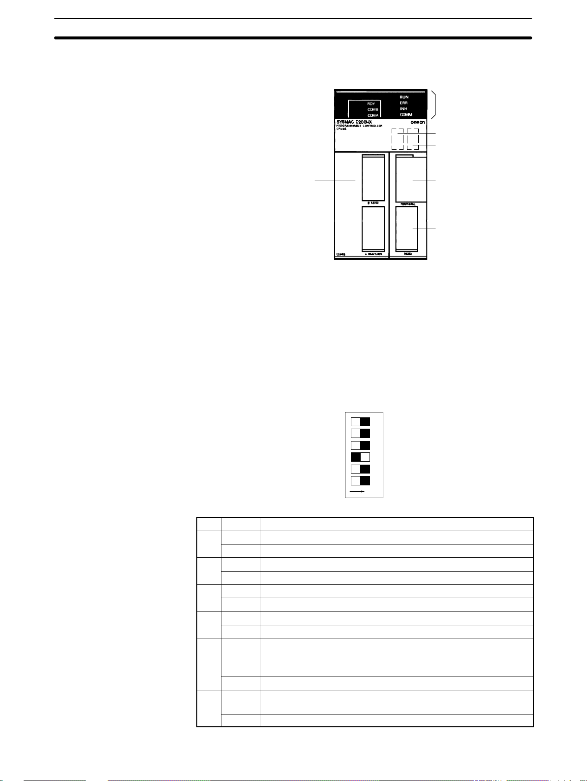
The following diagram shows the main CPU Unit components.
Indicators
Memory Cassette
DIP switch
Communications Board
(The C200HW-COM06-E
is mounted to this CPU
Unit.)
Peripheral port
RS-232C port
Memory Cassette The CPU Unit has a compartment to connect the Memory Cassette to the CPU
Unit. The Memory Cassette works as a RAM together with the built-in RAM of the
CPU Unit.
Peripheral Port A peripheral device can be connected to the peripheral port.
RS-232C Port The CPU Unit has a built-in RS-232C port.
Communications Board The CPU Unit has a compartment to connect the Communications Board to the
CPU Unit.
DIP Switch The PC operates according to the DIP switch settings of the CPU Unit. The DIP
switch of the CPU Unit for the C200HX/HG/HE has six pins. For the function of
each of the pins, refer to the following table. (All six pins are OFF when the PC is
shipped.)
123456
12
ON
OFF⇔ON
Pin Setting Function
1 ON Data cannot be written to the UM area.
OFF Data can be written to the UM area.
2 ON Memory Cassette data is read automatically at startup.
OFF Memory Cassette data is not read automatically at startup.
3 ON Programming Console displays messages in English.
OFF Programming Console displays messages in Japanese.
4 ON The expansion instructions can be set.
OFF The expansion instructions cannot be set (default setting).
5 ON Sets the following conditions for the communications port (including
when a CQM1-CIF02 is connected to the Peripheral Port):
1 start bit, 7 data bits, even parity, 2 stop bit, 9,600 bps baud rate
OFF Cancels the above settings.
6 ON Programming Console is in expansion terminal mode (AR 0712 is
turned ON).
OFF Programming Console is in normal mode (AR 0712 is turned OFF).
Page 25

CPU Unit Components Section 2-1
2-1-1 CPU Unit Indicators
CPU Unit indicators provide visual information on the general operation of the
PC. Although not substitutes for proper error programming using the flags and
other error indicators provided in the data areas of memory, these indicators provide ready confirmation of proper operation.
Indicator Meaning
RUN (green) Lit when the PC is operating normally.
ERR (red) Flashes if the PC detects any non-fatal error in operation. The PC
will continue operating.
Lit if the PC detects any fatal error in operation. The PC will stop
operating. After the PC stops operating, the RUN indicator will be
OFF and all output signals of the Output Units will be interrupted
(turned OFF).
INH (orange) Lit when the Load OFF flag (AR bit) is ON, in which case all
output signals of the Output Units will be interrupted (turned
OFF).
COMM
(orange)
Flashes when the CPU Unit is communicating with the device
connected to the peripheral port or RS-232C port.
2-1-2 Peripheral Device Connection
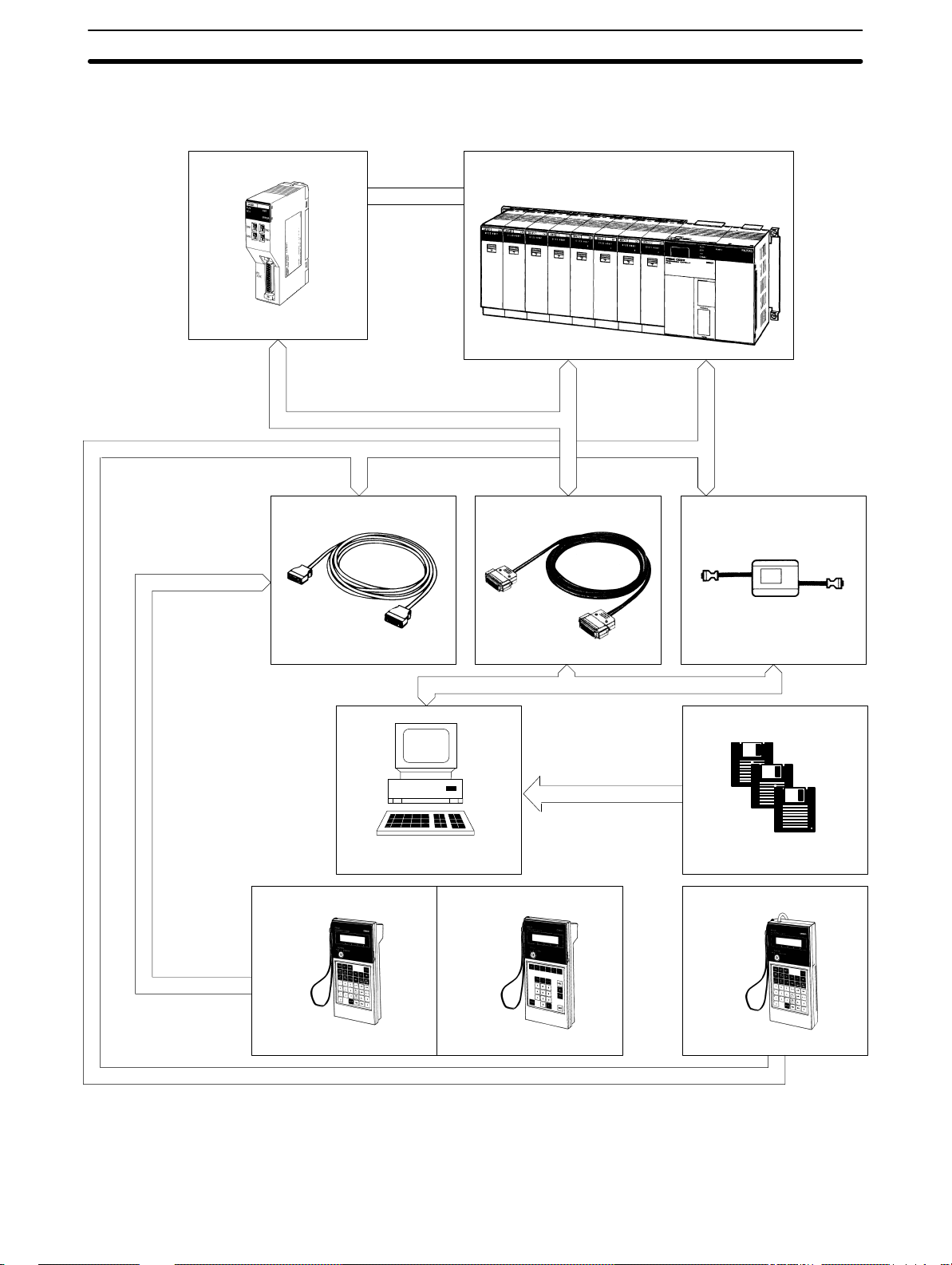
A Programming Console or IBM PC/AT running SSS can be used to program
and monitor the C200HX/HG/HE PCs.
Programming Console A C200H-PR027-E or CQM1-PRO01-E Programming Console can be con-
nected as shown in the diagram. The C200H-PR027-E is connected via the
C200H-CN222 or C200H-CN422 Programming Console Connecting Cable,
which must be purchased separately. A Connecting Cable is provided with the
CQM1-PRO01-E.
Data Access Console A C200H-DAC01 Data Access Console can be connected via the C200H-
CN222 or C200H-CN422 Programming Console Connecting Cable, which must
be purchased separately. The following operations are not available when the
C200H-DAC01 is used with the C200HX/HG/HE:
Set value read and change
Error message display
13
Page 26
CPU Unit Components Section 2-1
IBM PC/AT with SSS An IBM PC/AT or compatible computer with SYSMAC Support Software can be
connected as shown in the diagram.
C200H-LK201-V1
C200HX/HG/HE
Mounted
directly
Host Link Unit
Connecting
Cables
Peripheral
Device
C200H-CN222/422
(2 m/4 m)
Programming Console
Connecting Cable
XW2Z-200S/500S
(See note)
Connecting Cable
RS-232C
port
Support
Software
Peripheral
port
CQM1-CIF02
Connecting CableConnecting Cable
C500-ZL3AT1-E
14
IBM PC/AT or Compatible SYSMAC Support Software
Programming Console for
C200H
C200H-PRO27-E CQM1-PRO01-EC200H-DAC01
Data Access Console for
C200H
Programming Console
Note The connector of the XW2Z-200S/500S Connecting Cable is a male 25-pin ter-
minal. An adapter is required for the 9-pin male D-sub terminal on the IBM PC/AT
or compatible side.
Page 27
CPU Unit Capabilities Section 2-3
2-2 PC Configuration
The basic PC configuration consists of two types of Rack: a CPU Rack and Expansion I/O Racks. The Expansion I/O Racks are not a required part of the basic
system. They are used to increase the number of I/O points. An illustration of
these Racks is provided in 3-3 IR Area. A third type of Rack, called a Slave Rack,
can be used when the PC is provided with a Remote I/O System.
CPU Racks A C200HX/HG/HE CPU Rack consists of three components: (1) The CPU Back-
plane, to which the CPU Unit and other Units are mounted. (2) The CPU Unit,
which executes the program and controls the PC. (3) Other Units, such as I/O
Units, Special I/O Units, and Link Units, which provide the physical I/O terminals
corresponding to I/O points.
A C200HX/HG/HE CPU Rack can be used alone or it can be connected to other
Racks to provide additional I/O points. The CPU Rack provides three, five, eight,
or ten slots to which these other Units can be mounted depending on the backplane used.
Expansion I/O Racks An Expansion I/O Rack can be thought of as an extension of the PC because it
provides additional slots to which other Units can be mounted. It is built onto an
Expansion I/O Backplane to which a Power Supply and up to ten other Units are
mounted.
An Expansion I/O Rack is always connected to the CPU Unit via the connectors
on the Backplanes, allowing communication between the two Racks. Up to three
Expansion I/O Racks (two with the C200HE PCs) can be connected in series to
the CPU Rack.
Unit Mounting Position Only I/O Units and Special I/O Units can be mounted to Slave Racks. All I/O
Units, Special I/O Units, Group-2 High-density I/O Units, Remote I/O Master
Units, PC and Host Link Units, can be mounted to any slot on all other Racks.
Interrupt Input Units must be mounted to Backplanes with the “-V2” suffix on the
model number.
Refer to t h e C200HX/HG/HE Installation Guide for details about which slots can
be used for which Units and other details about PC configuration. The way in
which I/O points on Units are allocated in memory is described in 3-3 IR Area.
2-3 CPU Unit Capabilities
The following table shows the capabilities of the C200HX/HG/HE CPU Units.
The CPU4-E and CPU6-E CPU Units are equipped with RS-232C ports.
Item C200HE- C200HG- C200HX-
CPU11-E CPU32-E/
Program capacity 3.2K words 7.2K words 15.2K words 31.2K words
DM capacity 4K words 6K words 6K words 6K words
EM capacity None 6K words × 1 bank 6K words × 3 banks
Basic instruction execution time 0.3 µs min. 0.15 µs min. 0.1 µs min.
Max. number of Expansion I/O Racks 2 Racks 2 Racks 3 Racks 2 Racks 3 Racks
Max. number of Group-2 High-density I/O
Units
Max. number of Special I/O Units 10 Units 10 Units 16 Units 10 Units 16 Units
Clock function No Yes Yes Yes
Communications Board Slot No Yes Yes Yes
None 10 Units 10 Units 16 Units 10 Units 16 Units
42-E
CPU33-E/
43-E
CPU53-E/
63-E
CPU34-E/
44-E
CPU54-E/
64-E
15
Page 28
Memory Cassettes Section 2-4
2-4 Memory Cassettes
The C200HX/HG/HE comes equipped with a built-in RAM for the user’s program, so a normal program be created even without installing a Memory Cassette. An optional Memory Cassette can be used to store the program, PC Setup, I/O comments, DM area and other data area contents. Refer to the C200HX/
HG/HE Installation Guide for details on installing Memory Cassettes.
Memory Cassette Functions The Memory Cassette can be used to store and retrieve UM and IOM data; UM
stored in the Memory Cassette can also be compared to the UM in the PC.
1, 2, 3... 1. The contents of UM (user memory) can be stored in the Memory Cassette
for later retrieval or verification. If pin 2 of the CPU Unit DIP switch is set to
ON, the contents of the Memory Cassette are automatically retrieved when
the PC is turned ON.
The UM area contains the ladder program, fixed DM (such as the PC Setup),
expansion DM, I/O comments, the I/O table, and th e UM ar ea allocation information.
2. The contents of the PC’s I/O memory (IOM) can be stored in the Memory
Cassette for later retrieval.
Compatible Memory
Cassettes
IOM includes the IR area, SR area, LR area, HR area, AR area, timer and
counter PVs, DM 0000 through DM 6143, and EM 0000 through EM 6143.
UM and IOM data is completely compatible between the C200HX/HG/HE and
the C200HS data, except the portion of the C200HX/HG/HE data areas that exceed the capacity of the C200HS and the new instructions (BXF2(––),
IEMS(––), IORD(––), IOWR(––), PMCR(––), STUP(––), and XFR2(––)) that
aren’t supported by the C200HS CPU Unit. Data area addresses and instructions that aren’t supported by the C200HS can’t be used in the C200HS. IOM
data can ’t be retrieved to the PC’s RAM unless the size of the IOM in the Memory
Cassette matches the size of the IOM in the PC.
There are two types of Memory Cassette available: EEPROM and EPROM. The
following table shows the Memory Cassettes which can be used with the
C200HX/HG/HE PCs.
Memory Capacity Model number Comments
EEPROM
EPROM 16K or 32K
4K words C200HW-ME04K
8K words C200HW-ME08K
16K words C200HW-ME16K
32K words C200HW-ME32K
words
C200HS-MP16K The EPROM chip is not included
The EEPROM Memory Cassette
can be used to write and read UM
and I/O data to the CPU Unit. It does
and I/O data to the CPU Unit. It does
not require any backup power supply and will retain its data even after
it is removed from the CPU Unit.
with the Memory Cassette; it must
be purchased separately.
27256 equivalent (ROM-JD-B): 16K
27512 equivalent (ROM-KD-B): 32K
16
Note 1. Data stored in EEPROM won’t be reliable after the contents have been over-
written 50,000 times.
2. Use a standard PROM writer to write a program to the EPROM Memory
Cassette. Connect an EPROM to the EPROM Memory Cassette before
installing the EPROM Memory Cassette to the CPU Unit. The EPROM
Memory Cassette will lose its data if it is removed from the CPU Unit.
Page 29
Memory Cassettes Section 2-4
2-4-1 Hardware and Software Settings
The hardware and software settings related to Memory Cassette operations are
described below.
Switch Settings Switch 1 on the Memory Cassette is turned OFF when the Memory Cassette is
shipped. Check the setting on switch 1 before installation.
SR Area Flags and Control
Bits
Memory
Cassette
EEPROM
EPROM
SR 269 through SR 273 contain flags and control bits related to Memory Cassette contents and operation. Refer to 3-4 SR (Special Relay) Area for details.
Switch 1
ON The data in the Memory Cassette is write-protected.
OFF The data in the Memory Cassette can be overwritten.
ON 27512-equivalent ROM-KD-B EPROM
OFF 27256-equivalent ROM-JD-B EPROM
2-4-2 Writing/Reading UM Data
Use the following procedures to transfer UM data to or from a Memory Cassette.
(A PROM writer is required to write data to an EPROM Memory Cassette. Refer
to the SYSMAC Support Software Operation Manual for details.)
Note UM contains the ladder program, fixed DM (such as the PC Setup), expansion
DM, I/O comments, the I/O table, and the UM area allocation information.
Writing UM Data to a
Memory Cassette
1, 2, 3... 1. Before turning ON the C200HX/HG/HE’s power supply, make sure that
Reading UM Data from a
Memory Cassette
1, 2, 3... 1. Turn ON pin 2 of the CPU Unit’s DIP switch.
1, 2, 3... 1. Install the Memory Cassette containing the data into the C200HX/HG/HE.
Use the following procedure to write UM data to an EEPROM Memory Cassette.
switch 1 on the Memory Cassette is set to OFF.
2. Turn ON the C200HX/HG/HE and write the ladder program or read an existing program from a data disk.
3. Switch the C200HX/HG/HE to PROGRAM mode.
4. Use a host computer running SSS or a Programming Console to turn ON
SR 27000 (the Save UM to Cassette Bit). The data will be written from the
PC to the Memory Cassette. SR 27000 will be turned OFF automatically after the data transfer has been completed.
5. If you want to write-protect the data on the Memory Cassette, turn OFF the
PC and set switch 1 of the Memory Cassette to ON. If this switch is ON, data
in the Memory Cassette will be retained even if SR 27000 is turned ON.
There are two ways to read UM data from a Memory Cassette: automatic transfer at startup or a one-time transfer using a Peripheral Device.
(There is no function that automatically writes data to the Memory Cassette.)
Automatic Transfer at Startup:
2. Install the Memory Cassette containing the data into the C200HX/HG/HE.
3. Turn ON the C200HX/HG/HE’s power supply. The contents of the Memory
Cassette will be transferred to the CPU Unit automatically . A memory error
will occur if the data couldn’t be transferred.
One-time Transfer using a Peripheral Device:
2. Turn ON the C200HX/HG/HE and switch it to PROGRAM mode.
3. Use a host computer running SSS or a Programming Console to turn ON
SR 27001 (the Load UM from Cassette Bit). The data will be read from the
Memory Cass e t t e t o t h e PC. SR 27001 will be turned OFF automatically after the data transfer has been completed.
setting
Function
(32K words, 150 ns access time)
(16K words, 150 ns access time)
17
Page 30
Memory Cassettes Section 2-4
Comparing UM Data on a
Memory Cassette
Use the following procedure to the UM data on an Memory Cassette to the UM
data in the PC.
1, 2, 3... 1. Switch the C200HX/HG/HE to PROGRAM mode.
2. Use a host computer running SSS or a Programming Console to turn ON
SR 27002 (the Compare UM to Cassette Bit). The data will be compared between the PC and the Memory Cassette. SR 27002 will be turned OFF automatically after the data comparison has been completed.
3. Use a host computer running SSS or a Programming Console to check the
status of SR 27003 (the Comparison Results Flag).
Note If data verification is executed in a mode other than the PROGRAM mode, an
operation continuance error (FAL90) will occur and 27002 will turn ON (1). Although 27003 will also turn ON, comparison will not be performed. If data comparison is executed without mounting the Memory Cassette, 27003 will turn ON
(1).
2-4-3 Writing/Reading IOM Data
Use the following procedures to transfer IOM data to or from a Memory Cassette. (A PROM writer is required to write data to an EPROM Memory Cassette.
Refer to the SYSMAC Support Software Operation Manual for details.)
IOM includes the IR area, SR area, LR area, HR area, AR area, timer and counter PVs, DM 0000 through DM 6143, and EM 0000 through EM 6143.
The capacity of the Memory Cassette must match the memory capacity of the
CPU Unit when IOM data is transferred to or from a Memory Cassette. The
memory requirements are as follows:
Writing IOM: CPU Unit’s capacity ≤ Memory Cassette’s capacity
Reading IOM: CPU Unit’s capacity = Amount of IOM data in Memory Cas-
sette
Note In C200HS PCs, the data transfer will be performed even if the memory capaci-
ties don’t match, an error which can easily go unnoticed.
The following table shows the Memory Cassette capacity required to store 1 or
more banks of EM.
Writing IOM Data to a
Memory Cassette
18
Memory Cassette capacity Number of EM banks
4K words None (A 4K-word Memory Cassette can’t be used to
8K words None
16K words 1 bank (Only EM bank 0 can be stored.)
32K words 3 banks (EM banks 0 through 2 can be stored.)
store other IOM data, either.)
Bits 08 through 15 of SR 273 indicate the EM bank number of the IOM data
stored in the Memory Cassette.
Content of
SR 27308 to SR 27315
00 There is no Memory Cassette installed, no IOM data in
the Memory Cassette, or no EM data in the Memory Cassette.
01 The Memory Cassette contains IOM data that includes
EM bank 0 only.
04 The Memory Cassette contains IOM data that includes
EM banks 0 through 2.
Meaning
Use the following procedure to write IOM data to an EEPROM Memory Cassette.
1, 2, 3... 1. Before turning ON the C200HX/HG/HE’s power supply, make sure that
switch 1 on the Memory Cassette is set to OFF.
Page 31

Memory Cassettes Section 2-4
2. Turn ON the C200HX/HG/HE and switch it to PROGRAM mode.
3. Use a host computer running SSS or a Programming Console to turn ON
SR 27300 (the Save IOM to Cassette Bit). The data will be written from the
PC to the Memory Cassette. SR 27300 will be turned OFF automatically after the data transfer has been completed.
4. If you want to write-protect the data on the Memory Cassette, turn OFF the
PC and set switch 1 of the Memory Cassette to ON. If this switch is ON, data
in the Memory Cassette will be retained even if SR 27300 is turned ON.
Reading IOM Data from a
Memory Cassette
1, 2, 3... 1. Install the Memory Cassette containing the data into the C200HX/HG/HE.
Use the following procedure to read IOM data from a Memory Cassette. The
contents of the error history (DM 6000 through DM 6030) can’t be read from the
Memory Cassette.
Note There is no function that automatically reads IOM data from the Memory Cas-
sette.
2. Turn ON the C200HX/HG/HE and switch it to PROGRAM mode.
3. Use a host computer running SSS or a Programming Console to turn ON
SR 27301 (the Load IOM from Cassette Bit). The data will be read from the
Memory Cass e t t e t o t h e PC. SR 27301 will be turned OFF automatically after the data transfer has been completed.
19
Page 32

CPU Unit DIP Switch Section 2-5
2-5 CPU Unit DIP Switch
The 6 pins on the DIP switch control 6 of the CPU Unit’s operating parameters.
Pin Item Setting Function
1 Memory protect
2 Automatic transfer of Memory
Cassette contents
3 Message language
4 Expansion instruction setting
5 Communications parameters
6 Expansion TERMINAL mode
setting when AR 0712 is ON
ON The UM area1 cannot be overwritten from a Peripheral Device.
OFF The UM area1 can be overwritten from a Peripheral Device.
ON The contents of the Memory Cassette will be automatically
transferred to the internal RAM at start-up.
OFF The contents will not be automatically transferred.
ON Programming Console messages will be displayed in English.
OFF Programming Console messages will be displayed in the language
stored in system ROM. (Messages will be displayed in Japanese with
the Japanese version of system ROM.)
ON Expansion instructions will be set by user. Normally ON when using a
host computer for programming/monitoring.
OFF Expansion instructions will be set to defaults.
ON Standard communications parameters (see note 1) will be set for the
following serial communications ports.
• Built-in RS-232C port
• Peripheral port (only when a CQM1-CIF01/-CIF02 Cable is con-
nected. Does not apply to Programming Console.)
Note 1. Standard communications parameters are as follows:
Serial communications mode: Host Link or peripheral bus;
start bits: 1; data length: 7 bits; parity: even; stop bits: 2;
baud rate: 9,600 bps
2. The CX-Programmer running on a personal computer can
be connected to the peripheral port via the peripheral bus
using the above standard communications parameters.
OFF The communications parameters for the following serial
communications ports will be set in PC Setup as follows:
• Built-in RS-232C port: DM 6645 and DM 6646
• Peripheral port: DM 6650 and DM 6651
Note When the CX-Programmer is connected to the peripheral port
with the peripheral bus, either set bits 00 to 03 of DM 6650 in the
Fixed DM Area to 0 Hex (for standard parameters), or set bits 12
to 15 of DM 6650 to 0 Hex and bits 00 to 03 of DM 6650 to 1 Hex
(for Host Link or peripheral bus ) separately.
ON Expansion TERMINAL mode (Programming Console); AR 0712 ON.
OFF Normal mode (Programming Console); AR 0712: OFF
20
Note 1. The UM area contains the ladder program, fixed DM (including the PC Set-
up), expansion DM, I/O comments, the I/O table, and the UM area allocation
information.
2. All six pins are set to OFF when the PC is shipped.
Page 33

Operating without a Backup Battery Section 2-6
2-6 Operating without a Backup Battery
An EEPROM or EPROM Memory Cassette can be used together with various
memory settings to enable operation without a backup battery. The following
conditions must be met.
1, 2, 3... 1. The user program must be written to an EPROM or EEPROM Memory Cas-
sette.
2. The clock cannot be used. (A battery is required to run the internal clock.)
3. The PC Setup must be set to not detect low battery voltage.
4. The system must be designed to run properly even if DM area data is lost.
5. The Output OFF Bit (SR 25215) must be programmed to remain OFF. (The
status of this bit will be unstable without a battery.)
EEPROM Memory Cassette
1, 2, 3... 1. Allocate UM area using the SYSMAC Support Software (SSS) if you want to
25314 (Always OFF Flag)
25215
6. The Forced Status Hold Bit (SR 25211) and Data Retention Control Bit
(SR 25212) must be set to be cleared in the PC Setup. (The status of these
bits will be unstable without a battery.)
7. The DIP switch on the CPU Unit must be set so that pin 1 is OFF and pin 2 is
ON.
If these conditions can be met, use the following procedures to operate without a
backup battery.
use Expansion DM for Special I/O Units or if you want to store I/O comments
in the PC.
2. Write and transfer the user program, including a line using the Always OFF
Flag (SR 25314) to ensure that the Output OFF Bit (SR 25215) remains
OFF.
25314 (Always OFF Flag)
25215
3. Set the following in the PC Setup
DM 6601 = 0000 (To reset Forced Status Hold Bit (SR 25211) and I/O Status
Hold Bit (SR 25212) at startup)
DM 6655 bits 12 to 15 = 1, bits 4 to 7 = 0 ( To not detect low battery voltage)
DM 6600 and DM 6602 to DM 6654 = As required by the application.
4. Set Fixed DM (including the Communications Board settings in DM 6144 to
DM 6599) and Expansion DM as required by the application.
5. Check operation.
6. Mount the Memory Cassette in the CPU Unit.
7. Switch to PROGRAM mode.
8. Turn ON SR 27000 to transfer the program, Fixed DM, and the PC Setup to
the Memory Cassette. (This bit will automatically reset itself if turned ON
from a Programming Console. It will need to be turned OFF by clearing
forced status if it is set from the SSS.)
9. Turn ON the write protect switch on the Memory Cassette.
10. Turn OFF pin 1 and turn ON pin 2 on the DIP switch on the CPU Unit to automatically transfer the program, Fixed DM, and the PC Setup from the
Memory Cassette when power is turned ON.
21
Page 34

Operating without a Backup Battery Section 2-6
EPROM Memory Cassette
1, 2, 3... 1. Allocate UM area using the SYSMAC Support Software (SSS) if you want to
use Expansion DM for Special I/O Units or if you want to store I/O comments
in the PC.
2. Write and transfer the user program, including a line using the Always OFF
Flag (SR 25314) to ensure that the Output OFF Bit (SR 25215) remains
OFF.
25314 (Always OFF Flag)
25215
3. Set the following in the PC Setup
DM 6601 = 0000 (To reset Forced Status Hold Bit (SR 25211) and I/O Status
Hold Bit (SR 25212) at startup)
DM 6655 bits 12 to 15 = 1, bits 4 to 7 = 0 ( To not detect low battery voltage)
DM 6600 and DM 6602 to DM 6654 = As required by the application.
4. Set Fixed DM (including the Communications Board settings in DM 6144 to
DM 6599) and Expansion DM as required by the application.
5. Check operation.
6. Transfer the program, Fixed DM, and the PC Setup to the SSS.
7. Write the program, Fixed DM, and the PC Setup to ROM using the SSS and
a PROM writer.
8. Mount the ROM onto the Memory Cassette.
9. Mount the Memory Cassette in the CPU Unit.
10. Turn OFF pin 1 and turn ON pin 2 on the DIP switch on the CPU Unit to automatically transfer the program, Fixed DM, and the PC Setup from the
Memory Cassette when power is turned ON.
22
Page 35

SECTION 3
Memory Areas
Various types of data are required to achieve effective and correct control. T o facilitate managing this data, the PC is provided
with various memory areas for data, each of which performs a different function. The areas generally accessible by the user
for use in programming are classified as data areas. The other memory area is the UM Area, where the user’s program is
actually stored. This section describes these areas individually and provides information that will be necessary to use them. As
a matter of convention, the TR area is described in this section, even though it is not strictly a memory area.
3-1 Introduction 24. . . . . . . . . . . . . . . . . . . . . . . . . . . . . . . . . . . . . . . . . . . . . . . . . . . . . . . . . . . . . . . . . . . . . . . . . . . . .
3-1-1 Data Area Overview 24. . . . . . . . . . . . . . . . . . . . . . . . . . . . . . . . . . . . . . . . . . . . . . . . . . . . . . . . . . . . . .
3-1-2 IR/SR Area Overview 25. . . . . . . . . . . . . . . . . . . . . . . . . . . . . . . . . . . . . . . . . . . . . . . . . . . . . . . . . . . .
3-2 Data Area Structure 25. . . . . . . . . . . . . . . . . . . . . . . . . . . . . . . . . . . . . . . . . . . . . . . . . . . . . . . . . . . . . . . . . . . . . . .
3-3 IR (Internal Relay) Area 29. . . . . . . . . . . . . . . . . . . . . . . . . . . . . . . . . . . . . . . . . . . . . . . . . . . . . . . . . . . . . . . . . . .
3-4 SR (Special Relay) Area 33. . . . . . . . . . . . . . . . . . . . . . . . . . . . . . . . . . . . . . . . . . . . . . . . . . . . . . . . . . . . . . . . . . .
3-4-1 SYSMAC NET/SYSMAC LINK System 38. . . . . . . . . . . . . . . . . . . . . . . . . . . . . . . . . . . . . . . . . . . . .
3-4-2 Remote I/O Systems 39. . . . . . . . . . . . . . . . . . . . . . . . . . . . . . . . . . . . . . . . . . . . . . . . . . . . . . . . . . . . . .
3-4-3 Link System Flags and Control Bits 40. . . . . . . . . . . . . . . . . . . . . . . . . . . . . . . . . . . . . . . . . . . . . . . . .
3-4-4 Forced Status Hold Bit 41. . . . . . . . . . . . . . . . . . . . . . . . . . . . . . . . . . . . . . . . . . . . . . . . . . . . . . . . . . . .
3-4-5 I/O Status Hold Bit 42. . . . . . . . . . . . . . . . . . . . . . . . . . . . . . . . . . . . . . . . . . . . . . . . . . . . . . . . . . . . . . .
3-4-6 Output OFF Bit 42. . . . . . . . . . . . . . . . . . . . . . . . . . . . . . . . . . . . . . . . . . . . . . . . . . . . . . . . . . . . . . . . .
3-4-7 FAL (Failure Alarm) Area 42. . . . . . . . . . . . . . . . . . . . . . . . . . . . . . . . . . . . . . . . . . . . . . . . . . . . . . . . .
3-4-8 Low Battery Flag 42. . . . . . . . . . . . . . . . . . . . . . . . . . . . . . . . . . . . . . . . . . . . . . . . . . . . . . . . . . . . . . . .
3-4-9 Cycle Time Error Flag 43. . . . . . . . . . . . . . . . . . . . . . . . . . . . . . . . . . . . . . . . . . . . . . . . . . . . . . . . . . . .
3-4-10 I/O Verification Error Flag 43. . . . . . . . . . . . . . . . . . . . . . . . . . . . . . . . . . . . . . . . . . . . . . . . . . . . . . . . .
3-4-11 First Cycle Flag 43. . . . . . . . . . . . . . . . . . . . . . . . . . . . . . . . . . . . . . . . . . . . . . . . . . . . . . . . . . . . . . . . .
3-4-12 Clock Pulse Bits 43. . . . . . . . . . . . . . . . . . . . . . . . . . . . . . . . . . . . . . . . . . . . . . . . . . . . . . . . . . . . . . . . .
3-4-13 Step Flag 44. . . . . . . . . . . . . . . . . . . . . . . . . . . . . . . . . . . . . . . . . . . . . . . . . . . . . . . . . . . . . . . . . . . . . .
3-4-14 Group-2 Error Flag 44. . . . . . . . . . . . . . . . . . . . . . . . . . . . . . . . . . . . . . . . . . . . . . . . . . . . . . . . . . . . . . .
3-4-15 Special Unit Error Flag 44. . . . . . . . . . . . . . . . . . . . . . . . . . . . . . . . . . . . . . . . . . . . . . . . . . . . . . . . . . .
3-4-16 Instruction Execution Error Flag, ER 44. . . . . . . . . . . . . . . . . . . . . . . . . . . . . . . . . . . . . . . . . . . . . . . . .
3-4-17 Arithmetic Flags 44. . . . . . . . . . . . . . . . . . . . . . . . . . . . . . . . . . . . . . . . . . . . . . . . . . . . . . . . . . . . . . . . .
3-4-18 Interrupt Subroutine Areas 45. . . . . . . . . . . . . . . . . . . . . . . . . . . . . . . . . . . . . . . . . . . . . . . . . . . . . . . . .
3-4-19 RS-232C Port Communications Areas 45. . . . . . . . . . . . . . . . . . . . . . . . . . . . . . . . . . . . . . . . . . . . . . . .
3-4-20 Peripheral Port Communications Areas 46. . . . . . . . . . . . . . . . . . . . . . . . . . . . . . . . . . . . . . . . . . . . . . .
3-4-21 Memory Cassette Areas 46. . . . . . . . . . . . . . . . . . . . . . . . . . . . . . . . . . . . . . . . . . . . . . . . . . . . . . . . . . .
3-4-22 Data Transfer Error Bits 47. . . . . . . . . . . . . . . . . . . . . . . . . . . . . . . . . . . . . . . . . . . . . . . . . . . . . . . . . . .
3-4-23 Ladder Diagram Memory Areas 47. . . . . . . . . . . . . . . . . . . . . . . . . . . . . . . . . . . . . . . . . . . . . . . . . . . . .
3-4-24 Memory Error Flags 47. . . . . . . . . . . . . . . . . . . . . . . . . . . . . . . . . . . . . . . . . . . . . . . . . . . . . . . . . . . . . .
3-4-25 Data Save Flags 48. . . . . . . . . . . . . . . . . . . . . . . . . . . . . . . . . . . . . . . . . . . . . . . . . . . . . . . . . . . . . . . . .
3-4-26 Transfer Error Flags 48. . . . . . . . . . . . . . . . . . . . . . . . . . . . . . . . . . . . . . . . . . . . . . . . . . . . . . . . . . . . . .
3-4-27 PC Setup Error Flags 48. . . . . . . . . . . . . . . . . . . . . . . . . . . . . . . . . . . . . . . . . . . . . . . . . . . . . . . . . . . . .
3-4-28 Clock and Keyboard Mapping 48. . . . . . . . . . . . . . . . . . . . . . . . . . . . . . . . . . . . . . . . . . . . . . . . . . . . . .
3-4-29 Group-2 Error Flags 48. . . . . . . . . . . . . . . . . . . . . . . . . . . . . . . . . . . . . . . . . . . . . . . . . . . . . . . . . . . . . .
3-4-30 Special I/O Unit Restart Bits and Error Flags 48. . . . . . . . . . . . . . . . . . . . . . . . . . . . . . . . . . . . . . . . . .
3-5 AR (Auxiliary Relay) Area 48. . . . . . . . . . . . . . . . . . . . . . . . . . . . . . . . . . . . . . . . . . . . . . . . . . . . . . . . . . . . . . . . .
3-5-1 Restarting Special I/O Units 50. . . . . . . . . . . . . . . . . . . . . . . . . . . . . . . . . . . . . . . . . . . . . . . . . . . . . . . .
3-5-2 Slave Rack Error Flags 51. . . . . . . . . . . . . . . . . . . . . . . . . . . . . . . . . . . . . . . . . . . . . . . . . . . . . . . . . . . .
3-5-3 Group-2 Error Flags 51. . . . . . . . . . . . . . . . . . . . . . . . . . . . . . . . . . . . . . . . . . . . . . . . . . . . . . . . . . . . . .
3-5-4 Optical I/O Unit and I/O Terminal Error Flags 51. . . . . . . . . . . . . . . . . . . . . . . . . . . . . . . . . . . . . . . . .
3-5-5 SYSMAC LINK System Data Link Settings 52. . . . . . . . . . . . . . . . . . . . . . . . . . . . . . . . . . . . . . . . . . .
3-5-6 Error History Bits 52. . . . . . . . . . . . . . . . . . . . . . . . . . . . . . . . . . . . . . . . . . . . . . . . . . . . . . . . . . . . . . . .
3-5-7 Active Node Flags 52. . . . . . . . . . . . . . . . . . . . . . . . . . . . . . . . . . . . . . . . . . . . . . . . . . . . . . . . . . . . . . .
3-5-8 SYSMAC LINK/SYSMAC NET Link System Service Time 53. . . . . . . . . . . . . . . . . . . . . . . . . . . . . .
3-5-9 Calendar/Clock Area and Bits 53. . . . . . . . . . . . . . . . . . . . . . . . . . . . . . . . . . . . . . . . . . . . . . . . . . . . . .
3-5-10 TERMINAL Mode Key Bits 54. . . . . . . . . . . . . . . . . . . . . . . . . . . . . . . . . . . . . . . . . . . . . . . . . . . . . . .
3-5-11 Power OFF Counter 54. . . . . . . . . . . . . . . . . . . . . . . . . . . . . . . . . . . . . . . . . . . . . . . . . . . . . . . . . . . . . .
3-5-12 SYSMAC LINK – Peripheral Device Flags 54. . . . . . . . . . . . . . . . . . . . . . . . . . . . . . . . . . . . . . . . . . . .
3-5-13 Cycle Time Flag 55. . . . . . . . . . . . . . . . . . . . . . . . . . . . . . . . . . . . . . . . . . . . . . . . . . . . . . . . . . . . . . . . .
3-5-14 Link Unit Mounted Flags 55. . . . . . . . . . . . . . . . . . . . . . . . . . . . . . . . . . . . . . . . . . . . . . . . . . . . . . . . . .
3-5-15 CPU Unit-mounting Device Mounted Flag 55. . . . . . . . . . . . . . . . . . . . . . . . . . . . . . . . . . . . . . . . . . . .
3-5-16 FPD Trigger Bit 55. . . . . . . . . . . . . . . . . . . . . . . . . . . . . . . . . . . . . . . . . . . . . . . . . . . . . . . . . . . . . . . . .
3-5-17 Data Tracing Flags and Control Bits 55. . . . . . . . . . . . . . . . . . . . . . . . . . . . . . . . . . . . . . . . . . . . . . . . .
3-5-18 Cycle Time Indicators 55. . . . . . . . . . . . . . . . . . . . . . . . . . . . . . . . . . . . . . . . . . . . . . . . . . . . . . . . . . . .
3-6 DM (Data Memory) Area 56. . . . . . . . . . . . . . . . . . . . . . . . . . . . . . . . . . . . . . . . . . . . . . . . . . . . . . . . . . . . . . . . . .
3-6-1 Expansion DM Area 57. . . . . . . . . . . . . . . . . . . . . . . . . . . . . . . . . . . . . . . . . . . . . . . . . . . . . . . . . . . . . .
3-6-2 Special I/O Unit Data 58. . . . . . . . . . . . . . . . . . . . . . . . . . . . . . . . . . . . . . . . . . . . . . . . . . . . . . . . . . . . .
3-6-3 Error History Area 58. . . . . . . . . . . . . . . . . . . . . . . . . . . . . . . . . . . . . . . . . . . . . . . . . . . . . . . . . . . . . . .
3-6-4 PC Setup 60. . . . . . . . . . . . . . . . . . . . . . . . . . . . . . . . . . . . . . . . . . . . . . . . . . . . . . . . . . . . . . . . . . . . . . .
3-6-5 Communications Board Settings 65. . . . . . . . . . . . . . . . . . . . . . . . . . . . . . . . . . . . . . . . . . . . . . . . . . . .
3-6-6 Special I/O Unit Area Settings 67. . . . . . . . . . . . . . . . . . . . . . . . . . . . . . . . . . . . . . . . . . . . . . . . . . . . . .
3-7 HR (Holding Relay) Area 68. . . . . . . . . . . . . . . . . . . . . . . . . . . . . . . . . . . . . . . . . . . . . . . . . . . . . . . . . . . . . . . . . .
3-8 TC (Timer/Counter) Area 68. . . . . . . . . . . . . . . . . . . . . . . . . . . . . . . . . . . . . . . . . . . . . . . . . . . . . . . . . . . . . . . . . .
3-9 LR (Link Relay) Area 69. . . . . . . . . . . . . . . . . . . . . . . . . . . . . . . . . . . . . . . . . . . . . . . . . . . . . . . . . . . . . . . . . . . . .
3-10 UM Area 70. . . . . . . . . . . . . . . . . . . . . . . . . . . . . . . . . . . . . . . . . . . . . . . . . . . . . . . . . . . . . . . . . . . . . . . . . . . . . . .
3-11 TR (Temporary Relay) Area 71. . . . . . . . . . . . . . . . . . . . . . . . . . . . . . . . . . . . . . . . . . . . . . . . . . . . . . . . . . . . . . . .
3-12 EM (Extended Data Memory) Area 71. . . . . . . . . . . . . . . . . . . . . . . . . . . . . . . . . . . . . . . . . . . . . . . . . . . . . . . . . . .
3-12-1 Using the EM Area 71. . . . . . . . . . . . . . . . . . . . . . . . . . . . . . . . . . . . . . . . . . . . . . . . . . . . . . . . . . . . . .
3-12-2 The Current EM Bank 72. . . . . . . . . . . . . . . . . . . . . . . . . . . . . . . . . . . . . . . . . . . . . . . . . . . . . . . . . . . .
23
Page 36

Introduction Section 3-1
3-1 Introduction
3-1-1 Data Area Overview
Details, including the name, size, and range of each area are summarized in the
following table. Data and memory areas are normally referred to by their acronyms, e.g., the IR Area, the SR Area, etc.
Area Size Range Comments
Internal Relay Area 1 3,776 bits IR 000 to IR 235 Refer to 3-1-2 IR/SR Area Overview and 3-3 IR
Special Relay Area 1 312 bits SR 236 to SR 255
Special Relay Area 2 704 bits SR 256 to SR 299
Internal Relay Area 2 3,392 bits IR 300 to IR 511 Refer to 3-1-2 IR/SR Area Overview and 3-3 IR
Temporary Relay Area 8 bits TR 00 to TR 07 Used to temporarily store and retrieve execution
Holding Relay Area 1,600 bits HR 00 to HR 99 Used to store data and to retain the data values
Auxiliary Relay Area 448 buts AR 00 to AR 27 Contains flags and bits for special functions. Re-
Link Relay Area 1,024 bits LR 00 to LR 63 Used for data links in the PC Link System.
Timer/Counter Area 512 counters/
Data Memory Area
Fixed DM Area
Extended Data Memory
Area
timers
6,144 words DM 0000 to DM 6143 Read/Write
1,000 words DM 0000 to DM 0999 Normal DM.
2,600 words DM 1000 to DM 2599 Special I/O Unit Area
3,400 words DM 2600 to DM 5999 Normal DM.
31 words DM 6000 to DM 6030 History Log
(44 words) DM 6100 to DM 6143 Link test area (reserved)
512 words DM 6144 to DM 6599 Fixed DM Area (read only)
56 words DM 6600 to DM 6655 PC Setup
6,144 words EM 0000 to EM 6143 The amount of EM area memory depends on the
TC 000 to TC 511 Used to define timers and counters, and to
(Internal Relay) Area for more details.
Refer to 3-1-2 IR/SR Area Overview and 3-4 SR
(Special Relay) Area for more details.
(Internal Relay) Area for more details.
conditions when programming certain types of
branching ladder diagrams.
when the power to the PC is turned OFF.
tains status during power failure.
(These bits can be used as work words or work
bits when not used in the PC Link System.)
access completion flags, PV, and SV.
TIM 000 through TIM 015 are refreshed via
interrupt processing as high-speed timers.
DM 6031 is used for indirect DM addressing and
EM bank information and should not be written
by the user.
PC model being used. PCs are available with no
EM, one 6,144-word bank, or three 6,144-word
banks.
Like DM, the EM memory can be accessed in
word units only and EM area data is retained
when the power to the PC is turned OFF.
Work Bits and Words When some bits and words in certain data areas are not being used for their in-
tended purpose, they can be used in programming as required to control other
bits. Words and bits available for use in this fashion are called work words and
work bits. Most, but not all, unused bits can be used as work bits. Those that can
be used are described area-by-area in the remainder of this section. Actual application of work bits and work words is described in Section 4 Writing and Input-
ting the Program.
Flags and Control Bits Some data areas contain flags and/or control bits. Flags are bits that are auto-
matically turned ON and OFF to indicate particular operation status. Although
24
Page 37

Data Area Structure Section 3-2
some flags can be turned ON and OFF by the user, most flags are read only; they
cannot be controlled directly.
Control bits are bits turned ON and OFF by the user to control specific aspects o f
operation. Any bit given a name using the word bit rather than the word flag is a
control bit, e.g., Restart bits are control bits.
3-1-2 IR/SR Area Overview
When designating a data area, the acronym for the area is always required for
any area except the IR and SR areas. Although the acronyms for the IR and SR
areas are given for clarity in text explanations, they are not required, and not entered, when programming.
The IR and SR areas are divided into two 256-word sections; the boundary between these sections is located in the SR area between SR 255 and SR 256.
When the SR area is used as an operand in an instruction, the operand cannot
cross over this boundary. Also, basic instructions that access bits in the second
section (SR 25600 through IR 51115) have somewhat longer execution times.
Area Range Comments
IR Area 1
SR Area 1 SR 23600 to SR 25507 Contains system clocks, flags, control bits, and
SR Area 2 SR 256 to SR 299 Contains flags, control bits, and status informa-
IR Area 2
I/O Area 1 IR 000 to IR 029 I/O words are allocated to the CPU Rack and
Group-2 High-density I/O Unit
and B7A Interface Unit Area
SYSMAC BUS and
CompoBus/D Output Area
Special I/O Unit Area 1 IR 100 to IR 199 Allocated to Special I/O Units 0 to 9.
Optical I/O Unit and I/O
Terminal Area
Work Area IR 232 to IR 235 For use as work bits in the program.
I/O Area 2 IR 300 to IR 309 These I/O words are allocated to a third
Work Area IR 310 to IR 329 For use as work bits in the program.
Group-2 High-density I/O Unit
Area 2
Work Area IR 342 to IR 349 For use as work bits in the program.
CompoBus/D Input Area IR 350 to IR 399 Allocated to CompoBus/D inputs.
Special I/O Unit Area 2 IR 400 to IR 459 Allocated to Special I/O Units A to F.
Work Area IR 460 to IR 511 For use as work bits in the program.
IR 030 to IR 049 Allocated to Group-2 High-density I/O Units and to
IR 050 to IR 099 Allocated to CompoBus/D outputs and Remote
IR 200 to IR 231 Allocated to Optical I/O Units and I/O Terminals.
IR 330 to IR 341 Allocated to Group-2 High-density I/O Units.
Expansion I/O Racks by slot position.
B7A Interface Units 0 to 9.
I/O Slave Racks 0 to 4.
status information.
tion. SR 290 to SR 297 are used as I/O words by
MCRO(99).
Expansion I/O Rack by slot position.
Note 1. Refer to 3-3 IR (Internal Relay) Area for more details on the IR area.
Refer to 3-4 SR (Special Relay) Area for more details on the SR area.
2. Bits in IR Area 1 and IR Area 2 can can be used in programming as work bits
when not used for their allocated purpose.
3-2 Data Area Structure
When designating a data area, the acronym for the area is always required for
any but the IR and SR areas. Although the acronyms for the IR and SR areas are
often given for clarity in text explanations, they are not required, and not entered,
when programming. Any data area designation without an acronym is assumed
to be in either the IR or SR area. Because IR and SR addresses run consecutively, the word or bit addresses are sufficient to differentiate these two areas.
25
Page 38

Data Area Structure Section 3-2
An actual data location within any data area but the TC area is designated by its
address. The address designates the bit or word within the area where the desired data is located. The TC area consists of TC numbers, each of which is used
for a specific timer or counter defined in the program. Refer to 3-8 TC Area for
more details on TC numbers and to 5-14 Timer and Counter Instructions for information on their application.
The rest of the data areas (i.e., the IR, SR, HR, DM, AR, and LR areas) consist of
words, each of which consists of 16 bits numbered 00 through 15 from right to
left. IR words 000 and 001 are shown below with bit numbers. Here, the content
of each word is shown as all zeros. Bit 00 is called the rightmost bit; bit 15, the
leftmost bit.
The term least significant bit is often used for rightmost bit; the term most significant bit, for leftmost bit. These terms are not used in this manual because a
single data word is often split into two or more parts, with each part used for different parameters or operands. When this is done, the rightmost bits of a word
may actually become the most significant bits, i.e., the leftmost bits in another
word,when combined with other bits to form a new word.
Bit number
IR word 000 0000000000000000
IR word 001 0000000000000000
15 14 13 12 11 10 09 08 07 06 05 04 03 02 01 00
The DM area is accessible by word only; you cannot designate an individual bit
within a DM word. Data in the IR, SR, HR, AR, and LR areas is accessible either
by word or by bit, depending on the instruction in which the data is being used.
To designate one of these areas by word, all that is necessary is the acronym (if
required) and the two-, three-, or four-digit word address. To designate an area
by bit, the word address is combined with the bit number as a single four- or fivedigit address. The following table show examples of this. The two rightmost digits of a bit designation must indicate a bit between 00 and 15, i.e., the rightmost
digit must be 5 or less the next digit to the left, either 0 or 1.
The same TC number can be used to designate either the present value (PV) of
the timer or counter, or a bit that functions as the Completion Flag for the timer or
counter . This is explained in more detail in 3-8 TC Area.
Area Word designation Bit designation
IR 000 00015 (leftmost bit in word 000)
SR 252 25200 (rightmost bit in word 252)
DM DM 1250 Not possible
TC TC 215 (designates PV) TC 215 (designates completion flag)
LR LR 12 LR 1200
Data Structure Word data input as decimal values is stored in binary-coded decimal (BCD);
word data entered as hexadecimal is stored in binary form. Each four bits of a
word represents one digit, either a hexadecimal or decimal digit, numerically
equivalent to the value of the binary bits. One word of data thus contains four
digits, which are numbered from right to left. These digit numbers and the corresponding bit numbers for one word are shown below.
Digit number 3210
Bit number
Contents 0000000000000000
15 14 13 12 11 10 09 08 07 06 05 04 03 02 01 00
When referring to the entire word, the digit numbered 0 is called the rightmost
digit; the one numbered 3, the leftmost digit.
26
Page 39

Data Area Structure Section 3-2
When inputting data into data areas, it must be input in the proper form for the
intended purpose. This is no problem when designating individual bits, which
are merely turned ON (equivalent to a binary value of 1) or OFF (a binary value of
0). When inputting word data, however, i t i s important to input it either as decimal
or as hexadecimal, depending on what is called for by the instruction it is to be
used for. Section 5 Instruction Set specifies when a particular form of data is re-
quired for an instruction.
Converting Different Forms
of Data
Binary and hexadecimal can be easily converted back and forth because each
four bits of a binary number is numerically equivalent to one digit of a hexadecimal number. The binary number 0101111101011111 is converted to hexadecimal by considering each set of four bits in order from the right. Binary 1111 is
hexadecimal F; binary 0101 is hexadecimal 5. The hexadecimal equivalent
3
would thus be 5F5F, or 24,415 in decimal (16
x 5 + 162 x 15 + 16 x 5 + 15).
Decimal and BCD are easily converted back and forth. In this case, each BCD
digit (i.e., each group of four BCD bits) is numerically equivalent of the corresponding decimal digit. The BCD bits 0101011101010111 are converted to decimal by considering each four bits from the right. Binary 0101 is decimal 5; binary
0111 is decimal 7. The decimal equivalent would thus be 5,757. Note that this is
not the same numeric value as the hexadecimal equivalent of
0101011101010111, which would be 5,757 hexadecimal, or 22,359 in decimal
(163 x 5 + 162 x 7 + 16 x 5 + 7).
Because the numeric equivalent of each four BCD binary bits must be numerically equivalent to a decimal value, any four bit combination numerically greater
than 9 cannot be used, e.g., 1011 is not allowed because it is numerically equivalent to 11, which cannot be expressed as a single digit in decimal notation. The
binary bits 1011 are of course allowed in hexadecimal are a equivalent to the
hexadecimal digit C.
There are instructions provided to convert data either direction between BCD
and hexadecimal. Refer to 5-18 Data Conversion for details. Tables of binary
equivalents to hexadecimal and BCD digits are provided in the appendices for
reference.
Decimal Points Decimal points are used in timers only. The least significant digit represents
tenths of a second. All arithmetic instructions operate on integers only.
Signed and Unsigned Binary Data
This section explains signed and unsigned binary data formats. Many instructions can use either signed or unsigned data and a few (CPS(––), CPSL(––),
DBS(––), DBSL(––), MBS(––), and MBSL(––)) use signed data exclusively.
Unsigned binary Unsigned binary is the standard format used in OMRON PCs. Data in this manu-
al are unsigned unless otherwise stated. Unsigned binary values are always
positive and range from 0 ($0000) to 65,535 ($FFFF). Eight-digit values range
from 0 ($0000 0000) to 4,294,967,295 ($FFFF FFFF).
Digit value 16
Bit number
Contents 0000000000000000
15 14 13 12 11 10 09 08 07 06 05 04 03 02 01 00
3
16
2
16
1
16
0
27
Page 40

Data Area Structure Section 3-2
Signed Binary Signed binary data can have either a positive and negative value. The sign is
indicated by the status of bit 15. If bit 15 is OFF, the number is positive and if bit 15
is ON, the number is negative. Positive signed binary values range from 0
($0000) to 32,767 ($7FFF), and negative signed binary values range from
–32,768 ($8000) to –1 ($FFFF).
Sign indicator
Digit value 16
Bit number
Contents 0000000000000000
15 14 13 12 11 10 09 08 07 06 05 04 03 02 01 00
3
16
2
16
1
16
0
Eight-digit positive values range from 0 ($0000 0000) to 2,147,483,647 ($7FFF
FFFF), and eight-digit negative values range from –2,147,483,648 ($8000
0000) to –1 ($FFFF FFFF).
The following table shows the corresponding decimal, 16-bit hexadecimal, and
32-bit hexadecimal values.
Decimal 16-bit Hex 32-bit Hex
2147483647
2147483646
.
.
.
32768
32767
32766
.
.
.
2
1
0
–1
–2
.
.
.
–32767
–32768
–32769
.
.
.
–2147483647
–2147483648
---
---
--7FFF
7FFE
0002
0001
0000
FFFF
FFFE
8001
8000
---
---
---
.
.
.
.
.
.
.
.
.
.
.
.
7FFFFFFF
7FFFFFFE
.
.
.
00008000
00007FFF
00007FFE
.
.
.
00000002
00000001
00000000
FFFFFFFF
FFFFFFFE
.
.
.
FFFF8001
FFFF8000
FFFF7FFF
.
.
.
80000001
80000000
Converting Decimal to
Signed Binary
28
Positive signed binary data is identical to unsigned binary data (up to 32,767)
and can be converted using BIN(100). The following procedure converts negative decimal values between –32,768 and –1 to signed binary. In this example
–12345 is converted to CFC7.
Page 41

IR (Internal Relay) Area Section 3-3
1. First take the absolute value (12345) and convert to unsigned binary:
Bit number
Contents 0011000000111001
15 14 13 12 11 10 09 08 07 06 05 04 03 02 01 00
2. Next take the complement:
Bit number
Contents 1100111111000110
15 14 13 12 11 10 09 08 07 06 05 04 03 02 01 00
3. Finally add one:
Bit number
Contents 1100111111000111
15 14 13 12 11 10 09 08 07 06 05 04 03 02 01 00
Reverse the procedure to convert negative signed binary data to decimal.
3-3 IR (Internal Relay) Area
The IR area is used both as data to control I/O points, and as work bits to manipulate and store data internally. It is accessible both by bit and by word. In the
C200HX/HG/HE PC, the IR area is comprised of words IR 000 to IR 235 (IR
area 1) and IR 300 to IR 511 (IR area 2). Basic instructions have somewhat longer execution times when they access IR area 2 rather than IR area 1.
Words in the IR area that are used to control I/O points are called I/O words. Bits
in I/O words are called I/O bits. Bits in the IR area which are not assigned as I/O
bits can be used as work bits. IR area work bits are reset when power is interrupted or PC operation is stopped.
Area Range
IR Area 1
IR Area 2
I/O Area 1 IR 000 to IR 029
Group-2 High-density I/O Unit Area 1
and B7A Interface Unit Area
SYSMAC BUS and CompoBus/D Output
Area
Special I/O Unit Area 1 IR 100 to IR 199
Optical I/O Unit and I/O Terminal Area IR 200 to IR 231
Work Area IR 232 to IR 235
I/O Area 2 IR 300 to IR 309
Work Area IR 310 to IR 329
Group-2 High-density I/O Unit Area 2 IR 330 to IR 341
Work Area IR 342 to IR 349
CompoBus/D Input Area IR 350 to IR 399
Special I/O Unit Area 2 IR 400 to IR 459
Work Area IR 460 to IR 511
IR 030 to IR 049
IR 050 to IR 099
I/O Words If a Unit brings inputs into the PC, the bit assigned to it is an input bit; if the Unit
sends an output from the PC, the bit is an output bit. To turn ON an output, the
output bit assigned to it must be turned ON. When an input turns ON, the input bit
assigned to it also turns ON. These facts can be used in the program to access
input status and control output status through I/O bits.
Input Bit Usage Input bits can be used to directly input external signals to the PC and can be used
in any order in programming. Each input bit can also be used in as many instructions as required to achieve ef fective and proper control. They cannot be used in
29
Page 42

IR (Internal Relay) Area Section 3-3
instructions that control bit status, e.g., the OUTPUT, DIFFERENTIATION UP,
and KEEP instructions.
Output Bit Usage Output bits are used to output program execution results and can be used in any
order in programming. Because outputs are refreshed only once during each
cycle (i.e., once each time the program is executed), any output bit can be used
in only one instruction that controls its status, including OUT, KEEP(11),
DIFU(13), DIFD(14) and SFT(10). If an output bit is used in more than one such
instruction, only the status determined by the last instruction will actually be output from the PC.
See 5-15-1 Shift Register – SFT(10) for an example that uses an output bit in two
‘bit-control’ instructions.
Word Allocation for Racks I/O words are allocated to the CPU Rack and Expansion I/O Racks by slot posi-
tion. One I/O word is allocated to each slot, as shown in the following table. Since
each slot is allocated only one I/O word, a 3-slot rack uses only the first 3 words,
a 5-slot rack uses only the first 5 words, and an 8-slot rack uses only the first 8
words. Words that are allocated to unused or nonexistent slots are available as
work words.
Left side of rack Right side of a 10-slot rack →
←
Rack Slot 1 Slot 2 Slot 3 Slot 4 Slot 5 Slot 6 Slot 7 Slot 8 Slot 9 Slot 10
CPU IR 000 IR 001 IR 002 IR 003 IR 004 IR 005 IR 006 IR 007 IR 008 IR 009
1st Expansion IR 010 IR 011 IR 012 IR 013 IR 014 IR 015 IR 016 IR 017 IR 018 IR 019
2nd Expansion IR 020 IR 021 IR 022 IR 023 IR 024 IR 025 IR 026 IR 027 IR 028 IR 029
3rd Expansion IR 300 IR 301 IR 302 IR 303 IR 304 IR 305 IR 306 IR 307 IR 308 IR 309
Unused Words Any words allocated to a Unit that does not use them can be used in program-
ming as work words and bits. Units that do not used the words assigned to the
slot they are mounted to include Link Units (e.g., Host Link Units, PC Link Units,
SYSMAC NET Link Units, etc.), Remote I/O Master Units, Special I/O Units,
Group-2 High-density I/O Units, B7A Interface Units, and Auxiliary Power Supply Units.
Allocation for Special I/O
Units and Slave Racks
In most C200HX/HG/HE PCs, up to sixteen Special I/O Units may be mounted in
any slot of the CPU Rack or Expansion I/O Racks. (A limited number of Special
I/O Units can be installed in Remote I/O Slave Racks, too.) Each Special I/O Unit
is allocated ten words based on its unit number (0 to F).
Up to ten Special I/O Units may be mounted in the C200HE-CPU-E and
C200HG/HX-CPU3-E/4-E PCs. Each Unit is allocated ten words based on
its unit number (0 to 9).
Unit number I/O words PC Restrictions
0 IR 100 to IR 109
1 IR 110 to IR 119
2 IR 120 to IR 129
3 IR 130 to IR 139
4 IR 140 to IR 149
5 IR 150 to IR 159
6 IR 160 to IR 169
7 IR 170 to IR 179
8 IR 180 to IR 189
9 IR 190 to IR 199
None
30
Page 43

IR (Internal Relay) Area Section 3-3
Unit number PC RestrictionsI/O words
A IR 400 to IR 409
B IR 410 to IR 419
C IR 420 to IR 429
D IR 430 to IR 439
E IR 440 to IR 449
F IR 450 to IR 459
Note I/O words that aren’t allocated to Special I/O Units can be used as work words.
Up to five Slave Racks may be used, whether one or two Masters are used. IR
area words are allocated to Slave Racks by the unit number on the Unit, as
shown in the following tables.
Unit number I/O words
0 IR 050 to IR 059
1 IR 060 to IR 069
2 IR 070 to IR 079
3 IR 080 to IR 089
4 IR 090 to IR 099
Not available in C200HE-CPU-E and
C200HG/HX-CPU3-E/4-E PCs.
The C500-RT001/002-(P)V1 Remote I/O Slave Rack may be used, but it requires 20 I/O words, not 10, and therefore occupies the I/O words allocated to 2
C200H Slave Racks, both the words allocated to the unit number set on the rack
and the words allocated to the following unit number. When using a C200HX/
HG/HE CPU Unit, do not set the unit number on a C500 Slave Rack to 4, because there is no unit number 5. With the C500 Slave Rack, I/O words are allocated only to installed Units, from left to right, and not to slots as in the C200HX/
HG/HE Racks.
Allocation for Optical I/O
Units and I/O Terminals
I/O words between IR 200 and IR 231 are allocated to Optical I/O Units and I/O
Terminals by unit number. The I/O word allocated to each Unit is IR 200+n,
where n is the unit number set on the Unit.
Allocation for Remote I/O
Master and Link Units
Remote Master I/O Units and Host Link Units do not use I/O words, and the PC
Link Units use the LR area, so words allocated to the slots in which these Units
are mounted are available as work words.
Bit Allocation for I/O Units An I/O Unit may require anywhere from 8 to 16 bits, depending on the model.
With most I/O Units, any bits not used for input or output are available as work
bits. T ransistor Output Units C200H-OD213 and C200H-OD411, as well as Triac
Output Unit C200H-OA221, however, uses bit 08 for the Blown Fuse Flag. Transistor Output Unit C200H-OD214 uses bits 08 to 1 1 for the Alarm Flag. Bits 08 to
15 of any word allocated to these Units, therefore, cannot be used as work bits.
Bit Allocation for Interrupt
Input Units
The Interrupt Input Unit uses the 8 bits of the first I/O word allocated to its slot in
the CPU Rack. (An Interrupt Input Unit will operate as a normal Input Unit when
installed in an Expansion I/O Rack.) The other 24 bits allocated to its slot in the
CPU Rack can be used as work bits.
31
Page 44

IR (Internal Relay) Area Section 3-3
Allocation for Group-2
High-density I/O Units and
B7 Interface Units
Group-2 High-density I/O Units and B7A Interface Units are allocated words between IR 030 and IR 049 according to I/O number settings made on them and do
not use the words allocated to the slots in which they are mounted. For 32-point
Units, each Unit is allocated two words; for 64-point Units, each Unit is allocated
four words. The words allocated for each I/O number are in the following tables.
Any words or parts of words not used for I/O can be used as work words or bits in
programming.
32-point Units 64-point Units
I/O number Words I/O number Words
0 IR 30 to IR 31 0 IR 30 to IR 33
1 IR 32 to IR 33 1 IR 32 to IR 35
2 IR 34 to IR 35 2 IR 34 to IR 37
3 IR 36 to IR 37 3 IR 36 to IR 39
4 IR 38 to IR 39 4 IR 38 to IR 41
5 IR 40 to IR 41 5 IR 40 to IR 43
6 IR 42 to IR 43 6 IR 42 to IR 45
7 IR 44 to IR 45 7 IR 44 to IR 47
8 IR 46 to IR 47 8 IR 46 to IR 49
9 IR 48 to IR 49 9 Cannot be used.
A IR 330 to IR 331 A IR 330 to IR 333
B IR 332 to IR 333 B IR 332 to IR 335
C IR 334 to IR 335 C IR 334 to IR 337
D IR 336 to IR 337 D IR 336 to IR 339
E IR 338 to IR 339 E IR 338 to IR 341
F IR 340 to IR 341 F Cannot be used.
When setting I/O numbers on the High-density I/O Units and B7A Interface
Units, be sure that the settings will not cause the same words to be allocated to
more than o n e U n i t . F o r e x a m ple, if I/O number 0 is allocated to a 64-point Unit,
I/O number 1 cannot be used for any Unit in the system.
Group-2 High-density I/O Units and B7A Interface Units are not considered Special I/O Units and do not affect the limit to the number of Special I/O Units allowed
in the System, regardless of the number used.
The words allocated to Group-2 High-density I/O Units correspond to the connectors on the Units as shown in the following table.
Unit Word Connector/row
32-point Units
64-point Units
m Row A
m + 1 Row B
m CN1, row A
m + 1 CN1, row B
m + 2 CN2, row A
m + 3 CN2, row B
Note 1. Group-2 High-density I/O Units and B7A Interface Units cannot be mounted
to Slave Racks.
32
2. Refer to the Installation Guide for limitations on the number of Special I/O
Units that can be mounted to Slave Racks.
Page 45

SR (Special Relay) Area Section 3-4
3-4 SR (Special Relay) Area
The SR area contains flags and control bits used for monitoring PC operation,
accessing clock pulses, and signalling errors. SR area word addresses range
from 236 through 299; bit addresses, from 23600 through 29915.
The SR areas is divided into two sections. The first section ends at SR 255 and
the second section begins at SR 256. When an SR area word is used as an operand in an instruction, the operand mustn’t cross over this boundary. Basic
instructions that access bits in the SR Area 2 have longer execution times.
Area Range
SR Area 1 SR 23600 to SR 25507
SR Area 2 SR 25600 to SR 29915
The following table lists the functions of SR area flags and control bits. Most of
these bits are described in more detail following the table. Descriptions are in
order by bit number except that Link System bits are grouped together.
Unless otherwise stated, flags are OFF until the specified condition arises, when
they are turned ON. Restart bits are usually OFF, but when the user turns one
ON then OFF , the specified Link Unit will be restarted. Other control bits are OFF
until set by the user.
Not all SR words and bits are writeable by the user. Be sure to check the function
of a bit or word before attempting to use it in programming.
Word(s) Bit(s) Function
236
237
238 and 241 00 to 15 Data link status output area for operating level 0 of SYSMAC LINK or SYSMAC NET Link
242 and 245 00 to 15 Data link status output area for operating level 1 of SYSMAC LINK or SYSMAC NET Link
246 00 to 15 Not used
247 and 248
249 and 250
251
Writeable
Writeable
00 to 07 Node loop status output area for operating level 0 of SYSMAC NET Link System
08 to 15 Node loop status output area for operating level 1 of SYSMAC NET Link System
00 to 07 Completion code output area for operating level 0 following execution of
SEND(90)/RECV(98) for SYSMAC LINK/SYSMAC NET Link System or CMCR(––) for a PC
Card
08 to 15 Completion code output area for operating level 1 following execution of
SEND(90)/RECV(98) for SYSMAC LINK/SYSMAC NET Link System or CMCR(––) for a PC
Card
System
System
00 to 07 PC Link Unit Run Flags for Units 16 through 31 or data link status for operating level 1
08 to 15 PC Link Unit Error Flags for Units 16 through 31 or data link status for operating level 1
00 to 07 PC Link Unit Run Flags for Units 00 through 15 or data link status for operating level 0
08 to 15 PC Link Unit Error Flags for Units 00 through 15 or data link status for operating level 0
00 Remote I/O Error Read Bit
01 to 02 Not used
03 Remote I/O Error Flag
04 to 06 Slave Rack number and unit number of Remote I/O Unit, Optical I/O Unit, or I/O Terminal
with error
07 Not used
08 to 15 Master’s unit number and word allocated to Remote I/O Unit, Optical I/O Unit, or I/O Terminal
with error (Hexadecimal)
33
Page 46

SR (Special Relay) Area Section 3-4
Word(s) FunctionBit(s)
252
253
254
00 SEND(90)/RECV(98) Error Flag for operating level 0 of SYSMAC LINK or SYSMAC NET
Link System or CMCR(––) Error Flag for PC Card
01 SEND(90)/RECV(98) Enable Flag for operating level 0 of SYSMAC LINK or SYSMAC NET
Link System or CMCR(––) Enable Flag for PC Card
02 Operating Level 0 Data Link Operating Flag
03 SEND(90)/RECV(98) Error Flag for operating level 1 of SYSMAC LINK or SYSMAC NET
Link System or CMCR(––) Error Flag for PC Card
04 SEND(90)/RECV(98) Enable Flag for operating level 1 of SYSMAC LINK or SYSMAC NET
Link System or CMCR(––) Enable Flag for PC Card
05 Operating Level 1 Data Link Operating Flag
06 Rack-mounting Host Link Unit Level 1 Communications Error Flag
07 Rack-mounting Host Link Unit Level 1 Restart Bit
08 Peripheral Port Restart Bit
09 RS-232C Port Restart Bit
10 PC Setup Clear Bit
11 Forced Status Hold Bit
12 Data Retention Control Bit
13 Rack-mounting Host Link Unit Level 0 Restart Bit
14 Not used.
15 Output OFF Bit
00 to 07 FAL number output area (see error information provided elsewhere)
08 Low Battery Flag
09 Cycle Time Error Flag
10 I/O Verification Error Flag
11 Rack-mounting Host Link Unit Level 0 Communications Error Flag
12 Remote I/O Error Flag
13 Always ON Flag
14 Always OFF Flag
15 First Cycle Flag
00 1-minute clock pulse bit
01 0.02-second clock pulse bit
02 Negative (N) Flag
03 MTR Execution Flag
04 Overflow Flag (for signed binary calculations)
05 Underflow Flag (for signed binary calculations)
06 Differential Monitor End Flag
07 Step Flag
08 HKY Execution Flag
09 7SEG Execution Flag
10 DSW Execution Flag
11 Interrupt Input Unit Error Flag
12 Reserved by system (not accessible by user)
13 Interrupt Program Error Flag
14 Group-2 Error Flag
15 Special Unit Error Flag (includes Special I/O, PC Link, Host Link, Remote I/O Master Units)
34
Page 47

SR (Special Relay) Area Section 3-4
Word(s) FunctionBit(s)
255
256 to 261 00 to 15 Reserved by system
262 00 to 15 Longest interrupt subroutine (action) execution time (0.1-ms units)
263 00 to 15 Number of interrupt subroutine (action) with longest execution time. (8000 to 8255)
264
265 00 to 15 NT Link (1:N) Mode
266 00 to 15 Peripheral Reception Counter in RS-232C Mode
267
268 00 to 15 Communications Board Error Information
269
00 0.1-second clock pulse bit
01 0.2-second clock pulse bit
02 1.0-second clock pulse bit
03 Instruction Execution Error (ER) Flag
04 Carry (CY) Flag
05 Greater Than (GR) Flag
06 Equals (EQ) Flag
07 Less Than (LE) Flag
08 to 15 Reserved by system (used for TR bits)
(Bit 15 is the Interrupt Flag)
00 to 03 RS-232C Port Error Code
0: No error
2: Framing error
04 RS-232C Port Communications Error
05 RS-232C Port Send Ready Flag
06 RS-232C Port Reception Completed Flag
07 RS-232C Port Reception Overflow Flag
08 to 11 Peripheral Port Error Code in General I/O Mode
0: No error
2: Framing error
12 Peripheral Port Communications Error in General I/O Mode
13 Peripheral Port Send Ready Flag in in General I/O Mode
14 Peripheral Port Reception Completed Flag in General I/O Mode
15 Peripheral Port Reception Overflow Flag in General I/O Mode
Bits 00 to 07: Communicating with PT Flags for Units 0 to 7
Bits 08 to 15: Registering PT Priority Flags for Units 0 to 7
RS-232C Mode
Bits 00 to 15: RS-232C Port Reception Counter
00 to 04 Reserved by system (not accessible by user)
05 Host Link Level 0 Send Ready Flag
06 to 12 Reserved by system (not accessible by user)
13 Host Link Level 1 Send Ready Flag
14 to 15 Reserved by system (not accessible by user)
00 to 07 Memory Cassette Contents 00: Nothing; 01: UM; 02: IOM; 03: HIS
08 to 10 Memory Cassette Capacity
0: 0 KW (no cassette); 2: 4 or 8 KW; 3: 16 KW; 4: 32 KW
11 to 13 Reserved by system (not accessible by user)
14 EEPROM Memory Cassette Protected or EPROM Memory Cassette Mounted Flag
15 Memory Cassette Flag
These flags are turned OFF when the END(01)
instruction is executed, so their status can’t be
monitored from a Programming Console.
Refer to Appendix C for a table showing which
instructions affect these flags.
1: Parity error
3: Overrun error
1: Parity error
3: Overrun error
35
Page 48

SR (Special Relay) Area Section 3-4
Word(s) FunctionBit(s)
270
271
272
273
00 Save UM to Cassette Bit
01 Load UM from Cassette Bit
02 Compare UM to Cassette Bit
03 Comparison Results
0: Contents identical; 1: Contents differ or comparison not possible
04 to 10 Reserved by system (not accessible by user)
11 Transfer Error Flag: Transferring
SYSMAC NET data link table on UM
during active data link.
12 Transfer Error Flag: Not PROGRAM
mode
13 Transfer Error Flag: Read Only
14 Transfer Error Flag: Insufficient
Capacity or No UM
15 Transfer Error Flag: Board Checksum
Error
00 to 07 Ladder program size stored in Memory Cassette
Ladder-only File: 04: 4 KW; 08: 8 KW; 12: 12 KW; ... (32: 32 KW)
00: No ladder program or a file other than a ladder program has been stored.
08 to 15 Ladder program size and type in CPU Unit (Specifications are the same as for bits 00 to 07.)
00 to 10 Reserved by system (not accessible by user)
11 Memory Error Flag: PC Setup Checksum Error
12 Memory Error Flag: Ladder Checksum Error
13 Memory Error Flag: Instruction Change Vector Area Checksum Error
14 Memory Error Flag: Memory Cassette Online Disconnection
15 Memory Error Flag: Autoboot Error
00 Save IOM to Cassette Bit
01 Load IOM from Cassette Bit
02 Set this bit to 0.
03 to 07 Reserved by system (not accessible by user)
08 to 11 Contains the EM bank number when the Memory Cassette contains IOM data.
12 Transfer Error Flag: Not PROGRAM
mode
13 Transfer Error Flag: Read Only
14 Transfer Error Flag: Insufficient
Capacity or No IOM
15 Always 0.
Data transferred when the Bit is turned ON in
PROGRAM mode. Bit will automatically turn OFF.
PROGRAM mode. Bit will automatically turn OFF.
A non-fatal error will occur if these bits are turned
ON in RUN or MONITOR modes.
Data will not be transferred from UM to the Memory
Cassette if an error occurs (except for Board
Checksum Error). Detailed information on checksum
errors occurring in the Memory Cassette will not be
output to SR 272 because the information is not
needed. Repeat the transmission if SR 27015 is ON.
Data transferred to Memory Cassette when Bit is
turned ON in PROGRAM mode. Bit will automatically
turned ON in PROGRAM mode. Bit will automatically
turn OFF. An error will be produced if turned ON in
any other mode.
Data will not be transferred from IOM to the Memory
Cassette if an error occurs (except for Read Only
Error).
36
Page 49

SR (Special Relay) Area Section 3-4
Word(s) FunctionBit(s)
274
00 Special I/O Unit #0 Restart Flag
01 Special I/O Unit #1 Restart Flag
02 Special I/O Unit #2 Restart Flag
03 Special I/O Unit #3 Restart Flag
04 Special I/O Unit #4 Restart Flag
05 Special I/O Unit #5 Restart Flag
06 Special I/O Unit #6 Restart Flag
07 Special I/O Unit #7 Restart Flag
08 Special I/O Unit #8 Restart Flag
09 Special I/O Unit #9 Restart Flag
10 Special I/O Unit #A Restart Flag
11 Special I/O Unit #B Restart Flag
12 Special I/O Unit #C Restart Flag
13 Special I/O Unit #D Restart Flag
14 Special I/O Unit #E Restart Flag
15 Special I/O Unit #F Restart Flag
These flags will turn ON during restart processing.
These flags will not turn ON for Units on Slave
Racks.
275
276
277 to 279 00 to 15 Used for keyboard mapping. See page 412.
280 00 to 15 Group-2 High-density I/O Unit Error Flags for Units 0 to F
281 00 to 15 Special I/O Unit Restart Bits for Units 0 to F
282 00 to 15 Special I/O Unit Error Flags for Units 0 to F
283 to 286 00 to 15 Communications Board monitoring area
287 to 288 00 to 15 Communications Board interrupt data area
289
00 PC Setup Error (DM 6600 to DM 6605)
01 PC Setup Error (DM 6613 to DM 6623)
02 PC Setup Error (DM 6645 to DM 6655)
03 Reserved by system (not accessible by user)
04 Changing RS-232C Setup Flag
05 Reserved by system (not accessible by user)
06 to 07 Reserved by system (not accessible by user)
08 to 15 Reserved by system (not accessible by user)
00 to 07 Minutes (00 to 59)
08 to 15 Hours (00 to 23)
(AR 0205 to AR 0214 also function as Error Flags for Units 0 to 9.)
(Units 0 to 9 can also be restarted with Special I/O Unit Restart Bits AR 0100 to AR 0109.)
• To restart a Special I/O Unit, either use for force-set/reset operation to turn the Restart Bit ON
and OFF, or turn OFF the power and then turn it ON again.
• Follow the same procedure as above for starting PC Link Units.
(AR 0000 to AR 0009 also function as Error Flags for Units 0 to 9.)
00 to 07 Communications Board general monitoring area
08 Communications Board Port A Instruction Execution Flag
09 to 10 Used by Communications Board Port A instructions
11 Communications Board Port A Instruction Abort Bit
12 Communications Board Port B Instruction Execution Flag
13 to 14 Used by Communications Board Port B instructions
15 Communications Board Port B Instruction Abort Bit
Indicates the current time in BCD.
290 to 293 00 to 15 Macro Area inputs.
294 to 297 00 to 15 Macro Area outputs.
298 to 299 00 to 15 Reserved by system (not accessible by user)
37
Page 50

SR (Special Relay) Area Section 3-4
3-4-1 SYSMAC NET/SYSMAC LINK System
Loop Status SR 236 provides the local node loop status for SYSMAC NET Systems, as
shown below .
--- Bit in SR 236
Level 0 07 06 05 04 03 02 01 00
Level 1 15 14 13 12 11 10 09 08
Status/
Meaning
Completion Codes SR 23700 to SR23707 provide the SEND/RECV completion code for operating
1 1 Central Power Supply
0: Connected
1: Not connected
level 0 and SR 23708 to SR 23215 provide the SEND/RECV completion code for
operating level 1. The completion codes are as given in the following tables.
SYSMAC LINK
Code Item Meaning
00 Normal end Processing ended normally.
01 Parameter error Parameters for network communication instruction is
02 Unable to send Unit reset during command processing or local node
03 Destination not in
04 Busy error The destination node is processing data and cannot
05 Response timeout The response monitoring time was exceeded.
06 Response error There was an error in the response received from
07 Communications
08 Setting error There is an error in the node address settings.
09 PC error An error occurred in the CPU Unit of the destination
1 Loop Status
11: Normal loop
10: Downstream backloop
01: Upstream backloop
00: Loop error
network
controller error
Reception Status
0: Reception enabled
1: Reception disabled
not within acceptable ranges.
in not in network.
Destination node is not in network.
receive the command.
the destination node.
An error occurred in the communications controller.
node.
1
38
SYSMAC NET
Code Item Meaning
00 Normal end Processing ended normally.
01 Parameter error Parameters for network communication instruction is
02 Routing error There is a mistake in the routing tables for
03 Busy error The destination node is processing data and cannot
04 Send error (token
lost)
05 Loop error An error occurred in the communications loop.
06 No response The destination node does not exist or the response
07 Response error There is an error in the response format.
not within acceptable ranges.
connection to a remote network.
receive the command.
The token was not received from the Line Server.
monitoring time was exceeded.
Page 51

SR (Special Relay) Area Section 3-4
Data Link Status Flags SR 238 to SR 245 contain the data link status for SYSMAC LINK/SYSMAC NET
Systems. The data structure depends on the system used to create the data link.
SYSMAC LINK
Operating Operating
level 0 level 1
SR 238 SR 242 Node 4 Node 3 Node 2 Node 1
SR 239 SR 243 Node 8 Node 7 Node 6 Node 5
SR 240 SR 244 Node 12 Node 11 Node 10 Node 9
SR 241 SR 245 Node 16 Node 15 Node 14 Node 13
Leftmost bit Rightmost bit
1: Data link
operating
1: Communications error
12 to 15 11 to 08 04 to 07 00 to 03
1: PC CPU Unit
error
Bit
1: PC RUN status
SYSMAC NET
Operating Operating
level 0 level 1
SR 238 SR 242 8 7 6 5 4 3 2 1 8 7 6 5 4 3 2 1
SR 239 SR 243 16 15 14 13 12 11 10 9 16 15 14 13 12 11 10 9
SR 240 SR 244 24 23 22 21 20 19 18 17 24 23 22 21 20 19 18 17
SR 241 SR 245 32 31 30 29 28 27 26 25 32 31 30 29 28 27 26 25
15 14 13 12 11 10 09 08 07 06 05 04 03 02 01 00
1: PC CPU Unit error 1: PC RUN status
Bit (Node numbers below)
3-4-2 Remote I/O Systems
SR 25312 turns ON to indicate an error has occurred in Remote I/O Systems.
The ALM/ERR indicator will flash, but PC operation will continue. SR 251 contains information on the source and type of error and AR 0014 and AR 0015 contain information on the SYSMAC LINK status. The function of each bit is described below. Refer to Optical and Wired Remote I/O System Manuals for de-
tails.
SR 25100 – Error Check Bit If there are errors in more than one Remote I/O Unit, word SR 251 will contain
error information for only the first one. Data for the remaining Units will be stored
in memory and can be accessed by turning the Error Check bit ON and OFF. Be
sure to record data for the first error, which will be cleared when data for the next
error is displayed.
SR 25101 and SR 25102 Not used.
SR 25103 Remote I/O Error Flag: Bit 03 turns ON when an error has occurred in a Remote
I/O Unit.
SR 25104 through SR 25115 The content of bits 04 to 06 is a 3-digit binary number (04: 20, 05: 21, 06: 22) and
the content of bits 08 to 15 is a 2-digit hexadecimal number (08 to 11: 160, 12 to
15: 161).
If the content of bits 12 through 15 is B, an error has occurred in a Remote I/O
Master or Slave Unit, and the content of bits 08 through 1 1 will indicate the unit
number , either 0 or 1, of the Master involved. In this case, bits 04 to 06 contain
the unit number of the Slave Rack involved.
If the content of bits 12 through 15 is a number from 0 to 31, an error has occurred in a n Optical I/O Unit or I/O Terminal. The number is the unit number of the
Optical I/O Unit or I/O Terminal involved, and bit 04 will be ON if the Unit is assigned leftmost word bits (08 through 15), and OFF if it is assigned rightmost
word bits (00 through 07).
39
Page 52

SR (Special Relay) Area Section 3-4
3-4-3 Link System Flags and Control Bits
Use of the following SR bits depends on the configuration of any Link Systems to
which your PC belongs. These flags and control bits are used when Link Units,
such as PC Link Units, Remote I/O Units, or Host Link Units, are mounted to the
PC Racks or to the CPU Unit. For additional information, consult the System
Manual for the particular Units involved.
The following bits can be employed as work bits when the PC does not belong to
the Link System associated with them.
Host Link Systems
Both Error flags and Restart bits are provided for Host Link Systems. Error flags
turn ON to indicate errors in Host Link Units. Restart bits are turned ON and then
OFF to restart a Host Link Unit. SR bits used with Host Link Systems are summarized in the following table. Rack-mounting Host Link Unit Restart bits are
not effective for the Multilevel Rack-mounting Host Link Units. Refer to the
Host Link System Manual for details.
Bit Flag
25206 Rack-mounting Host Link Unit Level 1 Error Flag
25207 Rack-mounting Host Link Unit Level 1 Restart Bit
25213 Rack-mounting Host Link Unit Level 0 Restart Bit
25311 Rack-mounting Host Link Unit Level 0 Error Flag
PC Link Systems
PC Link Unit Error and Run
Flags
Single-level PC Link
Systems
When the PC belongs to a PC Link System, words 247 through 250 are used to
monitor the operating status of all PC Link Units connected to the PC Link System. This includes a maximum of 32 PC Link Units. If the PC is in a Multilevel PC
Link System, half of the PC Link Units will be in a PC Link Subsystem in operating
level 0; the other half, in a Subsystem in operating level 1. The actual bit assignments depend on whether the PC is in a Single-level PC Link System or a Multilevel PC Link System. Refer to the PC Link System Manual for details. Error and
Run Flag bit assignments are described below .
Bits 00 through 07 of each word are the Run flags, which are ON when the PC
Link Unit is in RUN mode. Bits 08 through 15 are the Error flags, which are ON
when an error has occurred in the PC Link Unit. The following table shows bit
assignments for Single-level and Multi-level PC Link Systems.
Flag type Bit no. SR 247 SR 248 SR 249 SR 250
Run flags 00 Unit #24 Unit #16 Unit #8 Unit #0
01 Unit #25 Unit #17 Unit #9 Unit #1
02 Unit #26 Unit #18 Unit #10 Unit #2
03 Unit #27 Unit #19 Unit #11 Unit #3
04 Unit #28 Unit #20 Unit #12 Unit #4
05 Unit #29 Unit #21 Unit #13 Unit #5
06 Unit #30 Unit #22 Unit #14 Unit #6
07 Unit #31 Unit #23 Unit #15 Unit #7
Error flags 08 Unit #24 Unit #16 Unit #8 Unit #0
09 Unit #25 Unit #17 Unit #9 Unit #1
10 Unit #26 Unit #18 Unit #10 Unit #2
11 Unit #27 Unit #19 Unit #11 Unit #3
12 Unit #28 Unit #20 Unit #12 Unit #4
13 Unit #29 Unit #21 Unit #13 Unit #5
14 Unit #30 Unit #22 Unit #14 Unit #6
15 Unit #31 Unit #23 Unit #15 Unit #7
40
Page 53

SR (Special Relay) Area Section 3-4
Multilevel PC Link Systems
Flag type Bit no. SR 247 SR 248 SR 249 SR 250
Run flags 00 Unit #8,
level 1
01 Unit #9,
level 1
02 Unit #10,
level 1
03 Unit #11,
level 1
04 Unit #12,
level 1
05 Unit #13,
level 1
06 Unit #14,
level 1
07 Unit #15,
level 1
Error flags 08 Unit #8,
level 1
09 Unit #9,
level 1
10 Unit #10,
level 1
11 Unit #11,
level 1
12 Unit #12,
level 1
13 Unit #13,
level 1
14 Unit #14,
level 1
15 Unit #15,
level 1
Unit #0,
level 1
Unit #1,
level 1
Unit #2,
level 1
Unit #3,
level 1
Unit #4,
level 1
Unit #5,
level 1
Unit #6,
level 1
Unit #7,
level 1
Unit #0,
level 1
Unit #1,
level 1
Unit #2,
level 1
Unit #3,
level 1
Unit #4,
level 1
Unit #5,
level 1
Unit #6,
level 1
Unit #7,
level 1
Unit #8,
level 0
Unit #9,
level 0
Unit #10,
level 0
Unit #11,
level 0
Unit #12,
level 0
Unit #13,
level 0
Unit #14,
level 0
Unit #15,
level 0
Unit #8,
level 0
Unit #9,
level 0
Unit #10,
level 0
Unit #11,
level 0
Unit #12,
level 0
Unit #13,
level 0
Unit #14,
level 0
Unit #15,
level 0
Unit #0,
level 0
Unit #1,
level 0
Unit #2,
level 0
Unit #3,
level 0
Unit #4,
level 0
Unit #5,
level 0
Unit #6,
level 0
Unit #7,
level 0
Unit #0,
level 0
Unit #1,
level 0
Unit #2,
level 0
Unit #3,
level 0
Unit #4,
level 0
Unit #5,
level 0
Unit #6,
level 0
Unit #7,
level 0
Application Example If the PC is in a Multilevel PC Link System and the content of word 248 is 02FF,
then PC Link Units #0 through #7 of in the PC Link Subsystem assigned operating level 1 would be in RUN mode, and PC Link Unit #1 in the same Subsystem
would have an error. The hexadecimal digits and corresponding binary bits of
word 248 would be as shown below.
Bit no. 15 00. . . . . . . . . . . . . . . . . . . . . . . . . . . . . . . . . . . . . . . . . . . . . . . . . . . .
Binary 0 0 0 0 0 0 1 0 1 1 1 1 1 1 1 1
Hex 0 2 F F
3-4-4 Forced Status Hold Bit
SR 25211 determines whether or not the status of bits that have been force-set
or force-reset is maintained when switching between PROGRAM and MONITOR mode to start or stop operation. If SR 25211 is ON, bit status will be maintained; if SR 25211 is OFF, all bits will return to default status when operation is
started or stopped. The Forced Status Hold Bit is only effective when enabled in
the PC Setup.
The status of SR 25211 in not affected by a power interruption unless the I/O
table is registered; in that case, SR 25211 will go OFF.
SR 25211 is not effective when switching to RUN mode.
SR 25211 should be manipulated from a Peripheral Device, e.g., a Program-
ming Console or SSS.
41
Page 54

SR (Special Relay) Area Section 3-4
Maintaining Status during
Startup
The status of SR 25211 and thus the status of force-set and force-reset bits can
be maintained when power is turned OFF and ON by enabling the Forced Status
Hold Bit in the PC Setup. If the Forced Status Hold Bit is enabled, the status of
SR 25211 will be preserved when power is turned OFF and ON. If this is done
and SR 25211 is ON, then the status of force-set and force-reset bits will also be
preserved, as shown in the following table.
ON ON Status maintained
OFF OFF Reset
Note Refer to 3-6-4 PC Setup for details on enabling the Forced Status Hold Bit.
3-4-5 I/O Status Hold Bit
SR 25212 determines whether or not the status of IR and LR area bits is maintained when operation is started or stopped. If SR 25212 is ON, bit status will be
maintained; i f S R 25212 is OFF, all IR and LR area bits will be reset. The I/O Status Hold Bit is effective only if enabled in the PC Setup.
The status of SR 25212 in not affected by a power interruption unless the I/O
table is registered; in that case, SR 25212 will go OFF.
SR 25212 should be manipulated from a Peripheral Device, e.g., a Programming Console or SSS.
Maintaining Status during
Startup
The status of SR 25212 and thus the status of IR and LR area bits can be maintained when power is turned OFF and ON by enabling the I/O Status Hold Bit in
the PC Setup. If the I/O Status Hold Bit is enabled, the status of SR 25212 will be
preserved when power is turned OFF and ON. If this is done and SR 25212 is
ON, then the status of IR and LR area bits will also be preserved, as shown in the
following table.
ON ON Status maintained
OFF OFF Reset
Status before shutdown Status at next startup
SR 25211 SR 25211 Force-set/reset bits
Status before shutdown Status at next startup
SR 25212 SR 25212 IR and LR bits
Note Refer to 3-6-4 PC Setup for details on enabling the I/O Status Hold Bit.
3-4-6 Output OFF Bit
SR bit 25215 is turned ON to turn OFF all outputs from the PC. The OUT INHIBIT
indicator on the front panel of the CPU Unit will light. When the Output OFF Bit is
OFF, all output bits will be refreshed in the usual way.
The status of the Output OFF Bit is maintained for power interruptions or when
PC operation is stopped, unless the I/O table has been registered, or the I/O
table has been registered and either the Forced Status Hold Bit or the I/O Status
Hold Bit has not been enabled in the PC Setup.
3-4-7 FAL (Failure Alarm) Area
A 2-digit BCD FAL code is output to bits 25300 to 25307 when the FAL or FALS
instruction is executed. These codes are user defined for use in error diagnosis,
although the PC also outputs FAL codes to these bits, such as one caused by
battery voltage drop.
This area can be reset by executing the F AL instruction with an operand of 00 or
by performing a Failure Read Operation from the Programming Console.
3-4-8 Low Battery Flag
SR bit 25308 turns ON if the voltage of the CPU Unit’s backup battery drops. The
ALM/ERR indicator on the front of the CPU Unit will also flash.
42
Page 55

SR (Special Relay) Area Section 3-4
This bit can be programmed to activate an external warning for a low battery voltage.
The operation of the battery alarm can be disabled in the PC Setup if desired.
Refer to 3-6-4 PC Setup for details.
3-4-9 Cycle Time Error Flag
SR bit 25309 turns ON if the cycle time exceeds 100 ms. The ALM/ERR indicator
on the front of the CPU Unit will also flash. Program execution will not stop, however, unless the maximum time limit set for the watchdog timer is exceeded. Timing may become inaccurate after the cycle time exceeds 100 ms.
3-4-10I/O Verification Error Flag
SR bit 25310 turns ON when the Units mounted in the system disagree with the
I/O table registered in the CPU Unit. The ALM/ERR indicator on the front of the
CPU Unit will also flash, but PC operation will continue.
To ensure proper operation, PC operation should be stopped, Units checked,
and the I/O table corrected whenever this flag goes ON.
3-4-11First Cycle Flag
SR bit 25315 turns ON when PC operation begins and then turns OFF after one
cycle of the program. The First Cycle Flag is useful in initializing counter values
and other operations. An example of this is provided in 5-14 Timer and Counter
Instructions.
3-4-12Clock Pulse Bits
Five clock pulses are available to control program timing. Each clock pulse bit is
ON for the first half of the rated pulse time, then OFF for the second half. In other
words, each clock pulse has a duty factor of 50%.
These clock pulse bits are often used with counter instructions to create timers.
Refer to 5-14 Timer and Counter Instructions for an example of this.
Pulse width 1 min 0.02 s 0.1 s 0.2 s 1.0 s
Bit 25400 25401 25500 25501 25502
Bit 25400
1-min clock pulse
30 s 30 s
1 min.
Bit 25500
0.1-s clock pulse
.05 s .05 s
0.1 s
Bit 25502
1.0-s clock pulse
0.5 s 0.5 s
1.0 s
.01 s .01 s
0.1 s 0.1 s
Note:
Because the 0.1-second and
0.02-second clock pulse bits have
ON times of 50 and 10 ms, respectively, the CPU Unit may not be
able to accurately read the pulses
if program execution time is too
long.
Bit 25401
0.02-s clock pulse
.02 s
Bit 25501
0.2-s clock pulse
0.2 s
43
Page 56

SR (Special Relay) Area Section 3-4
3-4-13Step Flag
SR bit 25407 turns ON for one cycle when step execution is started with the
STEP(08) instruction.
3-4-14Group-2 Error Flag
SR bit 25414 turns ON for any of the following errors for Group-2 High-density
I/O Units and B7A Interface Units: the same I/O number set twice, the same
words allocated to more than one Unit, refresh errors. If one of these errors occurs, the Unit will stop operation and the ALARM indicator will flash, but the overall PC will continue operation.
When the Group-2 Error Flag is ON, the number of the Unit with the error will be
provided in AR 0205 to AR 0214. If the Unit cannot be started properly even
though the I/O number is set correctly and the Unit is installed properly, a fuse
may be blown or the Unit may contain a hardware failure. If this should occur,
replace the Unit with a spare and try to start the system again.
There is also an error flag for High-density I/O Units and B7A Interface Units in
the AR area, AR 0215.
3-4-15Special Unit Error Flag
SR bit 25415 turns ON to indicate errors in the following Units: Special I/O, PC
Link, Host Link, and Remote I/O Master Units. SR bit 25415 will turn ON for any
of the following errors.
• When more than one Special I/O Unit is set to the same unit number.
• When an error occurs in refreshing data between a Special I/O Unit and the
PC’s CPU Unit.
• When an error occurs between a Host Link Unit and the PC’s CPU Unit.
• When an error occurs in a Remote I/O Master Unit.
Although the PC will continue operation if SR 25415 turns ON, the Units causing
the error will stop operation and the ALM indicator will flash. Check the status of
AR 0000 to AR 0015 to obtain the unit numbers of the Units for which the error
occurred and investigate the cause of the error.
Unit operation can be restarted by using the Restart Bits (AR 0100 to AR 0115,
SR 25207, and SR 25213), but will not be effective if the same unit number is set
for more than one Special I/O Unit. Turn OFF the power supply, correct the unit
number settings, and turn ON the power supply again to restart.
SR 25415 will not turn OFF even if AR 0100 to AR 0115 (Restart Bits) are turned
ON. It can be turned OFF by reading errors from a Programming Device or by
executing FAL(06) 00 from the ladder program.
3-4-16Instruction Execution Error Flag, ER
SR bit 25503 turns ON if an attempt is made to execute an instruction with incorrect operand data. Common causes of an instruction error are non-BCD operand data when BCD data is required, or an indirectly addressed DM word that is
non-existent. When the ER Flag is ON, the current instruction will not be
executed.
3-4-17Arithmetic Flags
The following flags are used in data shifting, arithmetic calculation, and comparison instructions. They are generally referred to only by their two-letter abbreviations.
Note These flags are all reset when the END(01) instruction is executed, and there-
fore cannot be monitored from a programming device.
Refer to 5-15 Data Shifting, 5-17 Data Comparison, 5-19 BCD Calculations, and
5-20 Binary Calculations for details.
44
Page 57

SR (Special Relay) Area Section 3-4
Negative Flag, N SR bit 25402 turns ON when the result of a calculation is negative.
Overflow Flag, OF SR bit 25404 turns ON when the result of a binary addition or subtraction ex-
ceeds 7FFF or 7FFFFFFF.
Underflow Flag, UF SR bit 25405 turns ON when the result of a signed binary addition or subtraction
exceeds 8000 or 80000000.
Carry Flag, CY SR bit 25504 turns ON when there is a carry in the result of an arithmetic opera-
tion or when a rotate or shift instruction moves a “1” into CY. The content of CY is
also used in some arithmetic operations, e.g., it is added or subtracted along
with other operands. This flag can be set and cleared from the program using the
Set Carry and Clear Carry instructions.
Greater Than Flag, GR SR bit 25505 turns ON when the result of a comparison shows the first of two
operands to be greater than the second.
Equal Flag, EQ SR bit 25506 turns ON when the result of a comparison shows two operands to
be equal or when the result of an arithmetic operation is zero.
Less Than Flag, LE SR bit 25507 turns ON when the result of a comparison shows the first of two
operands to be less than the second.
Note The four arithmetic flags are turned OFF when END(01) is executed.
3-4-18Interrupt Subroutine Areas
The following areas are used in subroutine interrupt processing.
Interrupt Subroutine
Maximum Processing Time
Area
Maximum Processing Time
Interrupt Subroutine
Number Area
SR bits 26200 to 26215 are used to set the maximum processing time of the interrupt subroutine. Processing times are determined to within 0.1 ms increments.
SR bits 26300 to 26315 contain the maximum processing time interrupt subroutine number. Bit 15 will be ON if there is an interruption.
3-4-19RS-232C Port Communications Areas
RS-232C Port Error Code SR bits 26400 to 26403 set when there is a RS-232C port error.
Error code Error type Error conditions Valid modes
0 No error --- All modes
1 Parity error When data received differs from
2 Framing error When step bit cannot be detected. All modes
3 Overrun error When data is not properly received. All modes
4 Timeout error When a timeout occurs for two PCs linked
RS-232C Port
Communication Error Bit
SR bit 26404 turns ON when there is a RS-232C port communication error .
positive/negative parity setting.
one-to-one.
All modes
1:1 PC Link slave or 1:1
PC Link master
RS-232C Port Send Ready
Flag
RS-232C Port Reception
Completed Flag
RS-232C Port Reception
Overflow Flag
RS-232C Reception Counter
SR bit 26405 turns ON when the PC is ready to transmit data.
SR bit 26406 turns ON when the PC has completed reading data from a
RS-232C device.
SR bit 26407 turns ON when data overflow occurs following the reception of
data.
SR 26500 to SR 26515 contains the number of RS-232C port receptions in General I/O Mode.
45
Page 58

SR (Special Relay) Area Section 3-4
Host Link Level 0 Send
SR bit 26705 turns ON when the PC is ready to transmit to the Host Link Unit.
Ready Flag
Host Link Level 1 Send
SR bit 26713 turns ON when the PC is ready to transmit to the Host Link.
Ready Flag
3-4-20Peripheral Port Communications Areas
Peripheral Port Error Code SR bits 26408 to 2641 1 are set when there is a peripheral port error in the Gener-
al I/O Mode.
Error code Error type Error conditions Valid modes
0 No error --- All modes
1 Parity error When data received differs from
2 Framing error When step bit cannot be detected. All modes
3 Overrun error When data is not properly received. All modes
4 Timeout error When a timeout occurs for two PCs linked
Peripheral Port
Communication Error Bit
Peripheral Port Send Ready
Flag
Peripheral Port Reception
Completed Flag
SR bit 26412 turns ON when there is a peripheral port communication error (effective in General I/O Mode).
SR bit 26413 turns ON when the PC is ready to transmit data in General I/O
Mode.
SR bit 26414 turns ON when the PC has completed reading data from a peripheral device. Effective in General I/O Mode.
positive/negative parity setting.
one-to-one.
All modes
1:1 PC Link slave or 1:1
PC Link master
Peripheral Port Reception
Overflow Flag
Peripheral Reception
Counter
Host Link Level 0 Send
SR bit 26415 turns ON when data overflow occurs following the reception of
data. Effective in General I/O Mode.
SR 26600 to SR 26615 contains the number of peripheral port receptions in
General I/O Mode (BCD).
SR bit 26705 turns ON when the PC is ready to transmit to the Host Link Unit.
Ready Flag
Host Link Level 1 Receive
SR bit 26713 turns ON when the PC is ready to receive data from the Host Link.
Ready Flag
3-4-21Memory Cassette Areas
Memory Cassette Contents SR 26900 to SR 26907 indicate the type of memory used for the Memory Cas-
sette.
Memory Type Code
Nothing 00
UM 01
IOM 02
HIS 03
Memory Cassette Capacity SR 26908 to SR 26910 indicate the memory capacity of the Memory Cassette.
Capacity Code
0 KW (no board mounted) 0
4 KW/8 KW 2
16 KW 3
32 KW 4
EEPROM/EPROM Memory
Cassette Mounted Flag
46
SR bit 26914 turns ON when EEPROM Memory Cassette is protected or
EPROM Memory Cassette is mounted.
Page 59

SR (Special Relay) Area Section 3-4
Memory Cassette Flag SR bit 26915 turns ON when a Memory Cassette is mounted.
Save UM to Cassette Flag SR bit 27000 turns ON when UM data is read to a Memory Cassette in Program
Mode. Bit will automatically turn OFF. An error will be produced if turned ON in
any other mode.
Load UM from Cassette
Flag
Collation (Between DM and
Memory Cassette)
SR bit 27001 turns ON when data is loaded into UM from a Memory Cassette in
Program Mode. Bit will automatically turn OFF. An error will be produced if
turned ON in any other mode.
SR bit 27002 turns ON when data has been compared between DM and a
Memory Cassette. SR bit 27003 is turned OFF if the data in the Memory Cassette matches and it is turned ON if the data does not match.
3-4-22Data Transfer Error Bits
Data will not be transferred from UM to the Memory Cassette if an error occurs
(except for Board Checksum Error). Detailed information on checksum errors
occurring in the Memory Cassette will not be output to SR 272 because the information is not needed. Repeat the transmission if SR 27015 is ON.
Transfer Error Flag:
Active Data Link
Transfer Error Flag:
Not PROGRAM Mode
Transfer Error Flag:
Read Only
Transfer Error Flag:
Insufficient Capacity or No
UM
SR bit 27011 turns ON when an attempt is made to transfer the UM used for the
SYSMAC NET data link table while the data link is active.
SR bit 27012 turns ON when the PC is not in Program Mode and data transfer is
attempted.
SR bit 27013 turns ON when the PC is in Read-only Mode and data transfer is
attempted.
SR bit 27014 turns ON when data transfer is attempted and available UM is insufficient.
Transfer Error Flag: Board
Checksum Error
SR bit 27015 turns ON when data transfer is attempted and a Board Checksum
error occurs.
3-4-23Ladder Diagram Memory Areas
Memory Cassette Ladder
Diagram Size Area
CPU Unit Ladder Diagram
Size and Type
SR 27100 to SR 27107 indicate the amount of ladder program stored in a
Memory Cassette. Ladder-only Files:
04: 4 KW; 08: 8 KW; 12: 12 KW; ... (32: 32 KW)
00:Memory Cassette contents not UM or there is no file.
SR 27108 to SR 27115 indicate the CPU Unit’s ladder program size and type.
Specifications are the same as for bits 00 to 07.
3-4-24Memory Error Flags
Memory Error Flag: PC
Setup Error
Memory Error Flag: Ladder
Checksum Error
Memory Error Flag:
Instruction Change Error
Memory Error Flag: Memory
Cassette Disconnect Error
SR bit 27211 turns ON when a PC Setup Checksum error occurs.
SR bit 27212 turns ON when a Ladder Checksum error occurs.
SR bit 27213 turns ON when an instruction change vector area error occurs.
SR bit 27214 turns ON when a Memory Cassette is connected or disconnected
during operations.
47
Page 60

AR (Auxiliary Relay) Area Section 3-5
Memory Error Flag:
Autoboot Error
SR bit 27215 turns ON when an autoboot error occurs.
3-4-25Data Save Flags
Data transferred to Memory Cassette when Bit is turned ON in PROGRAM
mode. Bit will automatically turn OFF. An error will be produced if turned ON in
any other mode.
Save IOM to Cassette Bit SR bit 27300 turns ON when IOM is saved to a Memory Cassette.
Load IOM from Cassette Bit SR bit 27301 turns ON when loading to IOM from a Memory Cassette.
3-4-26Transfer Error Flags
Data will not be transferred from IOM to the Memory Cassette if an error occurs
(except for Read Only Error).
Transfer Error Flag: Not
PROGRAM mode
Transfer Error Flag SR bit 27313 turns ON when attempting to transfer data in Read-only Mode.
Transfer Error Flag SR bit 27314 turns ON when attempting to transfer data and IOM capacity is in-
SR bit 27312 turns ON when attempting to transfer data in other than Program
Mode.
sufficient.
3-4-27PC Setup Error Flags
PC Setup Startup Error SR bit 27500 turns ON when a PC Setup Startup error occurs (DM6600 to
DM6605).
PC Setup RUN Error SR bit 27501 turns ON when a PC Setup Run error occurs (DM6613 to
DM6623).
PC Setup
Communications/Error
Setting/Misc. Error
SR bit 27502 turns ON when a PC Setup Communications, Error setting or Miscellaneous error occurs (DM 6635 to DM 6655).
3-4-28Clock and Keyboard Mapping
Clock (SR 276) SR 276 contains the current time. SR bits 27600 to 27607 contain the minutes
(00 to 59) and SR bits 27608 to 27615 contain the hours (0 to 23).
Keyboard Mapping (SR 277) SR 277 through SR 279 are used for keyboard mapping.
3-4-29Group-2 Error Flags
SR bits 28000 to SR 28015 are used as Error Flags for Group-2 High-density I/O
Units with unit numbers 0 to F. The corresponding Error Flag is turned ON when
an error occurs in that Unit. T en bits in the AR area (AR 0205 to AR 0214) are also
used as Error Flags for Units 0 to 9.
3-4-30Special I/O Unit Restart Bits and Error Flags
SR bits 28100 to SR 281 15 are used as Restart Bits for Special I/O Units with unit
numbers 0 to F. Turn the corresponding bit ON and OFF to restart a Special I/O
Unit. Ten bits in the AR area (AR 0100 to AR 0109) are also used as Restart Bits
for Units 0 to 9.
SR bits 28200 to SR 28215 are used as Error Flags for Special I/O Units with unit
numbers 0 to F. The corresponding Error Flag is turned ON when an error occurs
in that Unit. T en bits in the AR area (AR 0000 to AR 0009) are also used as Error
Flags for Units 0 to 9.
3-5 AR (Auxiliary Relay) Area
AR word addresses extend from AR 00 to AR 27; AR bit addresses extend from
AR 0000 to AR 2715. Most AR area words and bits are dedicated to specific
48
Page 61

AR (Auxiliary Relay) Area Section 3-5
uses, such as transmission counters, flags, and control bits, and words AR 00
through AR 0 7 and AR 23 through AR 27 cannot be used for any other purpose.
Words and bits from AR 08 to AR 17 are available as work words and work bits if
not used for the following assigned purposes.
Word Use
AR 08 to AR 15 SYSMAC LINK Units
AR 16, AR 17 SYSMAC LINK and SYSMAC NET Link Units
The AR area retains status during power interruptions, when switching from
MONITOR or RUN mode to PROGRAM mode, or when PC operation is
stopped. Bit allocations are shown in the following table and described in the following pages in order of bit number.
AR Area Flags and Control Bits
Word(s) Bit(s) Function
00 00 to 09 Error Flags for Special I/O Units 0 to 9 and PC Link Units 0 to 9
10 Error Flag for operating level 1 of SYSMAC LINK or SYSMAC NET Link System
11 Error Flag for operating level 0 of SYSMAC LINK or SYSMAC NET Link System
12 Host Computer to Rack-mounting Host Link Unit Level 1 Error Flag
13 Host Computer to Rack-mounting Host Link Unit Level 0 Error Flag
14 Remote I/O Master Unit 1 Error Flag
15 Remote I/O Master Unit 0 Error Flag
01 00 to 09 Restart Bits for Special I/O Units 0 to 9 and PC Link Units 0 to 9
10 Restart Bit for operating level 1 of SYSMAC LINK or SYSMAC NET Link System
11 Restart Bit for operating level 0 of SYSMAC LINK or SYSMAC NET Link System
12, 13 Not used.
14 Remote I/O Master Unit 1 Restart Bit.
15 Remote I/O Master Unit 0 Restart Bit.
02 00 to 04 Slave Rack Error Flags (#0 to #4)
05 to 14 Group-2 Error Flags (Bits 05 through 14 correspond to Units 0 to 9.)
15 Group-2 Error Flag
03 00 to 15 Error Flags for Optical I/O Units and I/O Terminals 0 to 7
04 00 to 15 Error Flags for Optical I/O Units and I/O Terminals 8 to 15
05 00 to 15 Error Flags for Optical I/O Units and I/O Terminals 16 to 23
06 00 to 15 Error Flags for Optical I/O Units and I/O Terminals 24 to 31
07
08 to 11 00 to 15 Active Node Flags for SYSMAC LINK System nodes of operating level 0
12 to 15 00 to 15 Active Node Flags for SYSMAC LINK System nodes of operating level 1
16 00 to 15 SYSMAC LINK/SYSMAC NET Link System operating level 0 service time per cycle
17 00 to 15 SYSMAC LINK/SYSMAC NET Link System operating level 1 service time per cycle
18
00 to 03 Data Link setting for operating level 0 of SYSMAC LINK System
04 to 07 Data Link setting for operating level 1 of SYSMAC LINK System
08 TERMINAL Mode Input Cancel Bit
09 Expansion TERMINAL Mode ON/OFF Bit
10 to 11 Not used.
12 Same as status of pin 6 on CPU Unit’s DIP switch
13 Error History Overwrite Bit
14 Error History Reset Bit
15 Error History Enable Bit
00 to 07 Seconds: 00 to 59
08 to 15 Minutes: 00 to 59
(The function of these flags is duplicated in SR 28200 through SR 28209.)
(The operation of these bits is duplicated in SR 28100 through SR 28109.)
49
Page 62

AR (Auxiliary Relay) Area Section 3-5
Word(s) FunctionBit(s)
19
20
21
22 00 to 15 Keyboard Mapping
23 00 to 15 Power Off Counter (BCD)
24
25
26 00 to 15 Maximum Cycle Time (0.1 ms)
27 00 to 15 Present Cycle Time (0.1 ms)
00 to 07 Hours: 00 to 23 (24-hour system)
08 to 15 Day of Month: 01 to 31 (adjusted by month and for leap year)
00 to 07 Month: 1 to 12
08 to 15 Year: 00 to 99 (Rightmost two digits of year)
00 to 07 Day of Week: 00 to 06 (00: Sunday; 01: Monday; 02: Tuesday; 03: Wednesday; 04:
Thursday; 05: Friday; 06: Saturday)
08 to 12 Not used.
13 30-second Compensation Bit
14 Clock Stop Bit
15 Clock Set Bit
00 SYSMAC LINK – RS-232C Peripheral Device Flag
01 SYSMAC LINK – Port A Peripheral Device Flag
02 SYSMAC LINK – Port B Peripheral Device Flag
03 SYSMAC LINK – Peripheral Device Initialization BIt
04 Not used.
05 Cycle Time Flag
06 SYSMAC LINK System Network Parameter Flag for operating level 1
07 SYSMAC LINK System Network Parameter Flag for operating level 0
08 SYSMAC LINK/SYSMAC NET Link Unit Level 1 Mounted Flag
09 SYSMAC LINK/SYSMAC NET Link Unit Level 0 Mounted Flag
10 Not used.
11 PC Link Unit Level 1 Mounted Flag
12 PC Link Unit Level 0 / Single Level Mounted Flag
13 Rack-mounting Host Link Unit Level 1 Mounted Flag
14 Rack-mounting Host Link Unit Level 0 Mounted Flag
15 CPU Unit-mounting Device Mounted Flag
00 to 07 Password for access to the Online Edit Disable Bit
(The Online Edit Disable Bit is valid when this byte contains 5A.)
08 FPD(––) Trigger Bit
09 Online Edit Disable Bit
10 Online Edit Standby Flag
11 Not used.
12 Trace End Flag
13 Tracing Flag
14 Trace Trigger Bit (writeable)
15 Trace Start Bit (writeable)
3-5-1 Restarting Special I/O Units
AR bits 0100 to AR 0109 correspond to the unit numbers of Special I/O Units 0 to
9. To restart Special I/O Units (including PC Link Units) turn the corresponding
bit ON and OFF (or turn power ON and OFF). Do not access data refreshed for
Special I/O Units during restart processing (see SR 27400 to SR 27409 on page
37).
Note Bits SR 28100 to SR 28115 also act as Restart Bits for Special I/O Units 0 to F.
50
Page 63

AR (Auxiliary Relay) Area Section 3-5
3-5-2 Slave Rack Error Flags
AR bits 0200 to AR 0204 correspond to the unit numbers of Remote I/O Slave
Units #0 to #4. These flags will turn ON if the same number is allocated to more
then one Slave or if a transmission error occurs when starting the System. Refer
to SR 251 for errors that occur after the System has started normally.
3-5-3 Group-2 Error Flags
Bits AR 0205 to AR 0215 correspond to Group-2 High-density I/O Units and B7A
Interface Units 0 to 9 (I/O numbers) and will turn ON when the same number is
set for more than one Unit, when the same word is allocated to more than one
Unit, when I/O number 9 is set for a 64-point Unit, or when the fuse burns out in a
Transistor High-density I/O Unit. AR bit 0215 will turn ON when a Unit is not recognized as a Group-2 High-density I/O Unit.
Note Bits SR 28000 to SR 28015 also act as Error Flags for Group-2 High-density I/O
Units with unit numbers 0 to F.
3-5-4 Optical I/O Unit and I/O Terminal Error Flags
AR 03 through AR 06 contain the Error Flags for Optical I/O Units and I/O T erminals. An error indicates a duplication of a unit number. Up to 64 Optical I/O Units
and I/O Terminals can be connected to the PC. Units are distinguished by unit
number , 0 through 31, and a letter, L or H. Bits are allocated as shown in the following table.
Optical I/O Unit and I/O
T erminal Error Flags
Bits AR03
allocation
00 0 L 8 L 16 L 24 L
01 0 H 8 H 16 H 24 H
02 1 L 9 L 17 L 25 L
03 1 H 9 H 17 H 25 H
04 2 L 10 L 18 L 26 L
05 2 H 10 H 18 H 26 H
06 3 L 11 L 19 L 27 L
07 3 H 11 H 19 H 27 H
08 4 L 12 L 20 L 28 L
09 4 H 12 H 20 H 28 H
10 5 L 13 L 21 L 29 L
11 5 H 13 H 21 H 29 H
12 6 L 14 L 22 L 30 L
13 6 H 14 H 22 H 30 H
14 7 L 15 L 23 L 31 L
15 7 H 15 H 23 H 31 H
AR04
allocation
AR05
allocation
AR06
allocation
51
Page 64

AR (Auxiliary Relay) Area Section 3-5
3-5-5 SYSMAC LINK System Data Link Settings
AR 0700 to AR 0703 and AR 0704 to AR 0707 are used to designate word allocations for operating levels 0 and 1 of the SYSMAC LINK System. Allocation can
be set to occur either according to settings from the SSS or automatically in the
LR and/or DM areas. If automatic allocation is designated, the number of words
to be allocated to each node is also designated. These settings are shown below.
External/Automatic
Allocation
Words per Node The following setting is necessary if automatic allocation is designated above.
Operating level 0 Operating level 1 Setting
AR 0700 AR 0701 AR 0704 AR 0705
0 0 0 0 Words set externally (SSS)
1 0 1 0 Automatic LR area only
0 1 0 1 allocation DM area only
1 1 1 1 LR and DM
Operating level 0 Operating level 1 Words per node Max. no.
AR 0702 AR 0703 AR 0706 AR 0707 LR area DM area
0 0 0 0 4 8 16
1 0 1 0 8 16 8
0 1 0 1 16 32 4
1 1 1 1 32 64 2
areas
of nodes
The above settings are read every cycle while the SYSMAC LINK System is in
operation.
3-5-6 Error History Bits
AR 0713 (Error History Overwrite Bit) is turned ON or OFF by the user to control
overwriting of records in the Error History Area in the DM area. T urn ON AR 0713
to overwrite the oldest error record each time an error occurs after 10 have been
recorded. Turn OFF AR 0713 to store only the first 10 records that occur each
time after the history area is cleared.
AR 0714 (Error History Reset Bit) is turned ON and then OFF by the user to reset
the Error Record Pointer (DM 6000) and thus restart recording error records at
the beginning of the history area.
AR 0715 (Error History Enable Bit) is turned ON by the user to enable error history storage and turned OFF to disable error history storage.
Refer to 3-6 DM Area for details on the Error History Area.
Error history bits are refreshed each cycle.
3-5-7 Active Node Flags
AR 08 through AR 1 1 and AR 12 through AR 15 provide flags that indicate which
nodes are active in the SYSMAC LINK System at the current time. These flags
are refreshed every cycle while the SYSMAC LINK System is operating.
The body of the following table show the node number assigned to each bit. If the
bit is ON, the node is currently active.
Level 0 Level 1 Bit (body of table shows node numbers)
00 01 02 03 04 05 06 07 08 09 10 11 12 13 14 15
AR 08 AR 12 1 2 3 4 5 6 7 8 9 10 11 12 13 14 15 16
AR 09 AR 13 17 18 19 20 21 22 23 24 25 26 27 28 29 30 31 32
AR 10 AR 14 33 34 35 36 37 38 39 40 41 42 43 44 45 46 47 48
AR 11 AR 15 49 50 51 52 53 54 55 56 57 58 59 60 61 62 * **
*Communication Controller Error Flag
**EEPROM Error Flag
52
Page 65

AR (Auxiliary Relay) Area Section 3-5
3-5-8 SYSMAC LINK/SYSMAC NET Link System Service Time
AR 16 provides the time allocated to servicing operating level 0 of the SYSMAC
LINK System and/or SYSMAC NET Link System during each cycle when a SYSMAC LINK Unit and/or SYSMAC NET Link Unit is mounted to a Rack.
AR 17 provides the time allocated to servicing operating level 1 of the SYSMAC
LINK System and/or SYSMAC NET Link System during each cycle when a SYSMAC LINK Unit and/or SYSMAC NET Link Unit is mounted to a Rack.
These times are recorded in 4-digit BCD to tenths of a millisecond (000.0 ms to
999.9 ms) and are refreshed every cycle.
Bits
15 to 12 11 to 08 07 to 04 03 to 00
10
2
10
1
10
0
10
–1
3-5-9 Calendar/Clock Area and Bits
Calendar/Clock Area A clock is built into the C200HX/HG/HE CPU Units. If AR 2114 (Clock Stop Bit) is
OFF, then the date, day, and time will be available in BCD in AR 18 to AR 20 and
AR 2100 to AR 2108 as shown below. This area can also be controlled with A R
2113 (30-second Compensation Bit) and AR 2115 (Clock Set Bit).
Calendar/Clock Bits
Bits Contents Possible values
AR 1800 to AR 1807 Seconds 00 to 59
AR 1808 to AR 1815 Minutes 00 to 59
AR 1900 to AR 1907 Hours 00 to 23 (24-hour system)
AR 1908 to AR 1915 Day of month 01 to 31 (adjusted by month and for leap year)
AR 2000 to AR 2007 Month 1 to 12
AR 2008 to AR 2015 Year 00 to 99 (Rightmost two digits of year)
AR 2100 to AR 2107 Day of week 00 to 06 (00: Sunday; 01: Monday; 02: Tuesday; 03: Wednesday; 04:
Thursday; 05: Friday; 06: Saturday)
30-second Compensation Bit AR 2113 is turned ON to round the seconds of the Calendar/clock Area to zero,
i.e., if the seconds is 29 or less, it is merely set to 00; if the seconds is 30 or greater, the minutes is incremented by 1 and the seconds is set to 00.
Clock Stop Bit AR 2114 is turned OFF to enable the operation of the Calendar/clock Area and
ON to stop the operation.
Clock Set Bit AR 2115 is used to set the Calendar/clock Area as described below. This data
must be in BCD and must be set within the limits for the Calendar/clock Area
given above.
1, 2, 3... 1. Turn ON AR 2114 (Stop Bit).
2. Set the desired date, day, and time, being careful not to turn OFF AR 2114
(Clock Stop Bit) when setting the day of the week (they’re in the same word).
(On the Programming Console, the Bit/Digit Monitor and Force Set/Reset
Operations are the easiest ways to set this data.)
3. Turn ON AR 2115 (Clock Set Bit). The Calendar/clock will automatically start
operating with the designated settings and AR 2114 and AR 2115 will both
be turned OFF.
The Calendar/clock Area and Bits are refreshed each cycle while operational.
Note The accuracy of the clock is as follows:
Temperature Accuracy/month
55°C –3 to 0 minutes
25°C ±1 minute
0°C –2 to 0 minutes
53
Page 66

AR (Auxiliary Relay) Area Section 3-5
3-5-10TERMINAL Mode Key Bits
If the Programming Console is mounted to the PC and is in TERMINAL mode,
any inputs on keys 0 through 9 (including characters A through F, i.e., keys 0
through 5 with SHIFT) will turn on a corresponding bit in AR 22. TERMINAL
mode is entered by a Programming Console operation.
The bits in AR 22 correspond to Programming Console inputs as follows:
Bit Programming Console input
AR 2200 0
AR 2201 1
AR 2202 2
AR 2203 3
AR 2204 4
AR 2205 5
AR 2206 6
AR 2207 7
AR 2208 8
AR 2209 9
AR 2210 A
AR 2211 B
AR 2212 C
AR 2213 D
AR 2214 E
AR 2215 F
Refer to Section 7 Program Monitoring and Execution for details on the TERMI-
NAL mode.
3-5-11Power OFF Counter
AR 23 provides in 4-digit BCD the number of times that the PC power has been
turned OFF. This counter can be reset as necessary using the PV Change 1 operation from the Programming Console. (Refer to 7-2-4 Hexadecimal/BCD Data
Modification for details.) The Power OFF Counter is refreshed every time power
is turned ON.
3-5-12SYSMAC LINK – Peripheral Device Flags
A Peripheral Device can be used through the SYSMAC LINK System from only
one port at a time. When changing the port from which the Peripheral Device is
being used, turn ON the SYSMAC LINK – Peripheral Device Initialization Bit
(AR 2403).
Bit Function
AR 2400 SYSMAC LINK – RS-232C Peripheral Device Flag
AR 2401 SYSMAC LINK – Port A Peripheral Device Flag
AR 2402 SYSMAC LINK – Port B Peripheral Device Flag
AR 2403 SYSMAC LINK – Peripheral Device Initialization Bit
(This flag is turned ON when a Peripheral Device is being used through
the SYSMAC LINK System from the RS-232C port.)
(This flag is turned ON when a Peripheral Device is being used through
the SYSMAC LINK System from Communications Board port A.)
(This flag is turned ON when a Peripheral Device is being used through
the SYSMAC LINK System form Communications Board port B.)
(Turn this bit ON to initialize the usage of a Peripheral Device through the
SYSMAC LINK System.)
54
Page 67

AR (Auxiliary Relay) Area Section 3-5
3-5-13Cycle Time Flag
AR 2405 turns ON when the cycle time set with SCAN(18) is shorter than the
actual cycle time.
AR 2405 is refreshed every cycle while the PC is in RUN or MONITOR mode.
3-5-14Link Unit Mounted Flags
The following flags indicate when the specified Link Units are mounted to the
Racks. (Refer to 3-5-15 CPU Unit-mounting Device Mounted Flag for CPU Unit-
mounting Host Link Units.) These flags are refreshed every cycle.
Name Bit Link Unit
SYSMAC LINK/SYSMAC NET Link Unit
Level 1 Mounted Flag
SYSMAC LINK/SYSMAC NET Link Unit
Level 0 Mounted Flag
Rack-mounting Host Link Unit Level 1 AR 2413 Rack-mounting Host Link Unit in operating level 1
Rack-mounting Host Link Unit Level 0 AR 2414 Rack-mounting Host Link Unit in operating level 0
AR 2408 SYSMAC LINK/SYSMAC NET Link Unit in operating level 1
AR 2409 SYSMAC LINK/SYSMAC NET Link Unit in operating level 0
3-5-15CPU Unit-mounting Device Mounted Flag
AR 2415 turns ON when any device is mounted directly to the CPU Unit. This
includes CPU Unit-mounting Host Link Units, Programming Consoles, and Interface Units. This flag is refreshed every cycle.
3-5-16FPD Trigger Bit
AR 2508 is used to adjust the monitoring time of FPD(––) automatically. Refer to
5-25-12 FAILURE POINT DETECT – FPD(––) for details.
3-5-17Data Tracing Flags and Control Bits
The following control bits and flags are used during data tracing with TRSM(45).
The Tracing Flag will be ON during tracing operations. The Trace Completed
Flag will turn ON when enough data has been traced to fill Trace Memory.
Bit Name
AR 2512 Trace Completed Flag
AR 2513 Tracing Flag
AR 2514 Trace Trigger Bit (writeable)
AR 2515 Sampling Start Bit (writeable)
Note Refer to 5-25-3 TRACE MEMORY SAMPLING – TRSM(45) for details.
3-5-18Cycle Time Indicators
AR 26 contains the maximum cycle time that has occurred since program execution was begun. AR 27 contains the present cycle time.
Both times are to tenths of a millisecond in 4-digit BCD (000.0 ms to 999.9 ms),
and are refreshed every cycle.
55
Page 68

DM (Data Memory) Area Section 3-6
3-6 DM (Data Memory) Area
The DM area is divided into various parts as described in the following table. A
portion of UM (up to 3,000 words in 1,000-word increments) can be allocated as
Expansion DM.
Addresses User
DM 0000 to DM 0999 Read/Write Normal DM.
DM 1000 to DM 2599
DM 2600 to DM 5999 Normal DM.
DM 6000 to DM 6030 History Log
DM 6100 to DM 6143 Reserved
DM 6144 to DM 6599 Read only System Settings
DM 6600 to DM 6655 PC Setup
DM 7000 to DM 9999 Expansion DM
read/write
Special I/O Unit Area
Usage
1
2
Note 1. The PC Setup can be set to use DM 7000 through DM 8599 as the Special
I/O Area instead of DM 1000 to DM 2599. Refer to 3-6-4 PC Setup for de-
tails.
When Special I/O Units are used, 100 words are occupied by each Unit, as
follows:
Unit #0: DM 1000 to DM 1099
Unit #1: DM 1100 to DM 1199
(...)
Unit #9: DM 1900 to DM 1999
Unit #A: DM 2000 to DM 2099
(...)
Unit #F: DM 2500 to DM 2599
2. The UM Area Allocation Programming Console operation can be used to allocate up to 3000 words of UM as Expansion DM.
Although composed of 16-bit words like any other data area, data in the DM area
cannot be specified by bit for use in instructions with bit operands. DM 0000 to
DM 6143 can be written to by the program, but DM 6144 to DM 6655 can be overwritten only from a Peripheral Device, such as a Programming Console or computer with SSS.
The DM area retains status during power interruptions.
DM 6031 cannot be used in user applications because it is used by the system to
store EM bank number information and indirect DM addresses.
Indirect Addressing Normally, when the content of a data area word is specified for an instruction, the
instruction is performed directly on the content of that word. For example, suppose MOV(21) is performed with DM 0100 as the first operand and LR 20 as the
second operand. When this instruction is executed, the content of DM 0100 is
moved to LR 20.
Note Expansion DM cannot be used for indirect addressing.
It is possible, however, to use indirect DM addresses as the operands for many
instructions. To indicate an indirect DM address, DM is input with the address of
the operand. With an indirect address, with content of this operand does not contain the actual data to be used. Instead, its contents is assumed to hold the address of another DM word, the content of which will actually be used in the
instruction. If DM 0100 was used in our example above and the content of DM
0100 is 0324, then DM 0100 actually means that the content of DM 0324 is to
56
Page 69

DM (Data Memory) Area Section 3-6
be used as the operand in the instruction, and the content of DM 0324 will be
moved to LR 00.
3-6-1 Expansion DM Area
The expansion DM area is designed to provide memory space for storing operating parameters and other operating data for Link Units and Special I/O Units.
Up to 3,000 words of UM can be allocated as Expansion DM (in 1K-word increments) using the UM ALLOCATION operation in the Programming Console or
SSS. Expansion DM area addresses run from DM 7000 to DM 9999.
The data in the expansion DM area can be transferred to the Special I/O Unit
Default Area (DM 1000 to DM 1999) when starting the PC or via programming
instruction to easily change operating parameters, enabling rapid switching between control processes. The expansion DM area can also be used to store parameters for other devices connected in the PC system, e.g., Programmable
Terminal character string or numeral tables.
The expansion DM area is used to store operating parameters and cannot be
used in programming like the normal DM area. Expansion DM can only be overwritten from a Peripheral Device, retains status during power interruptions, and
cannot be used for indirect addressing.
The UM area can be allocated as expansion DM area in increments of 1K words.
Once expansion DM area has been created, it is saved and transferred as part of
the program, i.e., no special procedures are required when saving or transferring the program.
MOV(21)
DM 0100
LR 00
Indirect
address
Word Content
DM 0099 4C59
DM 0100 0324
DM 0101 F35A
DM 0324 5555
DM 0325 2506
DM 0326 D541
Indicates
DM 0324
5555 moved
to LR 00.
UM ALLOCATION Operation The procedure for the Programming Console’s UM ALLOCATION operation is
shown below. Refer to 4-6-3 Clearing Memory for details on the DATA CLEAR
and UM ALLOCATION instructions.
1, 2, 3... 1. Clear memory.
CLR
NOT
RESETSET
EXT MONTR
Note UM allocation is not possible unless memory is cleared first.
2. The expansion DM area can be set to 0, 1, 2, or 3 K words. The following key
sequence creates a 2-KW expansion DM area (DM 7000 to DM 8999).
WRITECLR FUN VER CHG 2 SET 9 7 1 3
Press the 0 Key to eliminate the expansion DM area (0 KW).
or Press the 1 Key to allocate DM 7000 to DM 7999 (1 KW).
or Press the 2 Key to allocate DM 7000 to DM 8999 (2 KW).
or Press the 3 Key to allocate DM 7000 to DM 9999 (3 KW).
57
Page 70

DM (Data Memory) Area Section 3-6
3-6-2 Special I/O Unit Data
Special I/O Units are allocated 1000 or 1600 words in the DM Area depending on
the value set in word DM 6602 of the PC Setup. The DM 6602 setting determines
whether the Special I/O Unit Data area is setup for 10 or 16 Units and whether
the data is stored in read/write DM (DM 1000 to DM 2599) or read-only DM
(DM 7000 to DM 8599). Refer to Appendix E for details.
Unit Addresses
0 DM 1000 to DM 1099 or DM 7000 to DM 7099
1 DM 1100 to DM 1199 or DM 7100 to DM 7199
2 DM 1200 to DM 1299 or DM 7200 to DM 7299
3 DM 1300 to DM 1399 or DM 7300 to DM 7399
4 DM 1400 to DM 1499 or DM 7400 to DM 7499
5 DM 1500 to DM 1599 or DM 7500 to DM 7599
6 DM 1600 to DM 1699 or DM 7600 to DM 7699
7 DM 1700 to DM 1799 or DM 7700 to DM 7799
8 DM 1800 to DM 1899 or DM 7800 to DM 7899
9 DM 1900 to DM 1999 or DM 7900 to DM 7999
A DM 2000 to DM 2099 or DM 8000 to DM 8099
B DM 2100 to DM 2199 or DM 8100 to DM 8199
C DM 2200 to DM 2299 or DM 8200 to DM 8299
D DM 2300 to DM 2399 or DM 8300 to DM 8399
E DM 2400 to DM 2499 or DM 8400 to DM 8499
F DM 2500 to DM 2599 or DM 8500 to DM 8599
Note These DM words can be used for other purposes when not allocated to Special
I/O Units.
3-6-3 Error History Area
DM 6000 to DM 6030 are used to store up to 10 records that show the nature,
time, and date of errors that have occurred in the PC.
The Error History Area will store system-generated or FAL(06)/FALS(07)-generated error codes whenever AR 0715 (Error History Enable Bit) is ON. Refer to
Section 9 Troubleshooting for details on error codes.
Area Structure Error records occupy three words each stored between DM 6001 and DM 6030.
The last record that was stored can be obtained via the content of DM 6000 (Error Record Pointer). The record number, DM words, and pointer value for each of
the ten records are as follows:
Record Addresses Pointer value
None N.A. 0000
1 DM 6001 to DM 6003 0001
2 DM 6004 to DM 6006 0002
3 DM 6007 to DM 6009 0003
4 DM 6010 to DM 6012 0004
5 DM 6013 to DM 6015 0005
6 DM 6016 to DM 6018 0006
7 DM 6019 to DM 6021 0007
8 DM 6022 to DM 6024 0008
9 DM 6025 to DM 6027 0009
10 DM 6028 to DM 6030 000A
58
Page 71

DM (Data Memory) Area Section 3-6
Although each of them contains a dif ferent record, the structure of each record is
the same: the first word contains the error code; the second and third words, the
day and time. The error code will be either one generated by the system or by
FAL(06)/FALS(07); the time and date will be the date and time from AR 18 and
AR 19 (Calender/date Area). Also recorded with the error code is an indication of
whether the error is fatal (08) or non-fatal (00). This structure is shown below.
Word Bit Content
First 00 to 07 Error code
08 to 15 00 (non-fatal) or 80 (fatal)
Second 00 to 07 Seconds
08 to 15 Minutes
Third 00 to 07 Hours
08 to 15 Day of month
The following table lists the possible error codes and corresponding errors.
Error severity Error code Error
Fatal errors 00 Power interruption
01 to 99 or 9F System error (FALS)
C0 to C3 I/O bus error
E0 Input-output I/O table error
E1 Too many Units
F0 No END(01) instruction
F1 Memory error
Non-fatal errors 01 to 99 System error (FAL)
8A Interrupt Input error
8B Interrupt program error
9A Group 2 High-density I/O error
9B PC Setup error
9C Communications Board error
9D UM Memory Cassette transfer error
B0 to B1 Remote I/O error
D0 Special I/O error
E7 I/O table verification error
F7 Battery error
F8 Cycle time overrun
Operation When the first error code is generated with AR 0715 (Error History Enable Bit)
turned ON, the relevant data will be placed in the error record after the one indicated by the History Record Pointer (initially this will be record 1) and the Pointer
will be incremented. Any other error codes generated thereafter will be placed in
consecutive records until the last one is used. Processing of further error records
is based on the status of AR 0713 (Error History Overwrite Bit).
If AR 0713 is ON and the Pointer contains 000A, the next error will be written into
record 10, the contents of record 10 will be moved to record 9, and so on until the
contents of record 1 is moved off the end and lost, i.e., the area functions like a
shift register . The Record Pointer will remain set to 000A.
If AR 0713 is OFF and the Pointer reaches 000A, the contents of the Error History Error will remain as it is and any error codes generate thereafter will not be
recorded until AR 0713 is turned OFF or until the Error History Area is reset.
59
Page 72

DM (Data Memory) Area Section 3-6
The Error History Area can be reset by turning ON and then OFF
AR 0714 (Error History Reset Bit). When this is done, the Record Pointer will be
reset to 0000, the Error History Area will be reset (i.e., cleared), and any further
error codes will be recorded from the beginning of the Error History Area.
AR 0715 (Error History Enable Bit) must be ON to reset the Error History Area.
3-6-4 PC Setup
The PC Setup (DM 6600 through DM 6655) contains settings that determine PC
operation. Data in the PC Setup can be changed with a Programming Console or
SSS if UM is not write-protected by pin 1 of the CPU Unit’s DIP switch. Refer to
page 20 for details on changing DIP switch pin settings.
The data in DM 6600 through DM 6634 can be set or changed only when the PC
is in PROGRAM mode. The data in DM 6635 through DM 6655 can be set or
changed when the PC is in PROGRAM or MONITOR mode. The following words
can be changed from the SYSMAC Support Software’s PC Setup menu. (The
PC must be in PROGRAM mode.)
1, 2, 3... 1. Startup mode (DM 6600)
2. Startup mode designation (DM 6601)
3. Cycle monitor time (DM 6618)
4. Cycle time setting (DM 6619)
5. RS-232C Port Settings (DM 6645 through DM 6649)
The PC can be operated with the default PC Setup, which requires changing
only when customizing the PC’s operating environment to application needs.
The PC Setup parameters are described in the following table.
If there is an error in the settings in DM 6600 to DM 6655, a non-fatal error (error
code 9B) will occur when the data is read by the PC and one of the flags from
SR 27500 to SR 27502 will turn ON to indicate the location of the error. If there is
an error in the settings in DM 6550 to DM 6559, a non-fatal error (error code 9C)
will occur.
Word(s) Bit(s) Function Default
Startup Processing (DM 6600 to DM 6612)
The following settings are accessed only once when the PC is turned ON.
DM 6600 00 to 07 Startup mode (effective when bits 08 to 15 are set to 02).
00: PROGRAM; 01: MONITOR 02: RUN
08 to 15 Startup mode designation
00: Programming Console switch
01: Continue operating mode last used before power was turned off
02: Setting in 00 to 07
DM 6601 00 to 07 Reserved ---
08 to 11 IOM Hold Bit (SR 25212) Status
0: Reset; 1: Maintain
12 to 15 Forced Status Hold Bit (SR 25211) Status
0: Reset; 1: Maintain
PROGRAM
Programming
Console switch
Reset
60
Page 73

DM (Data Memory) Area Section 3-6
Word(s) DefaultFunctionBit(s)
DM 6602 00 to 07 Not used. ---
08 to 15 00: C200H-compatible RAM Mode (Default)
DM 6603 to
DM 6604
DM 6605 00 to 07 Momentary power interruption time (0 to 10 ms)
DM 6606 to
DM 6612
Communications and Cycle Time Settings (DM 6613 to DM 6619)
The following settings are accessed only once when program execution begins.
DM 6613 00 to 07 Servicing time for Communications Board port B
00 to 15 Not used. ---
08 to 15 Not used. --00 to 15 Not used. ---
08 to 15 Communications Board port B servicing setting enable
Use DM 1000 through DM 2599 for the initial data area for the Special
I/O Unit Area.
• Data in the Special I/O Unit Area can be read/written.
• The data cannot be converted to ROM.
01: C200H-compatible ROM Mode 1
Transfer the contents of DM 7000 through DM 7999 to DM 1000
through DM 1999 at startup and use DM 1000 through DM 1999.
• The UM Area Allocation operation must be performed beforehand.
• The data is compatible with C200H applications that use EEPROM/
EPROM.
• ROM conversion is possible indirectly by writing DM 7000 through DM
7999 to ROM.
02: DM Linear Mode 1
Use DM 7000 through DM 7999 for the initial data area for Special I/O
Unit Area.
• The UM Area Allocation operation must be performed beforehand.
• DM 1000 through DM 1999 can be used as regular DM.
• DM 7000 through DM 7999 can be converted to ROM.
11: C200H-compatible ROM Mode 2
Transfer the contents of DM 7000 through DM 8599 to DM 1000
through DM 2599 at startup and use DM 1000 through DM 2599.
• The UM Area Allocation operation must be performed beforehand.
• ROM conversion is possible indirectly by converting DM 7000 through
DM 8599 to ROM.
12: DM Linear Mode 2
Use DM 7000 through DM 8599 for the Special I/O Unit Area.
• The UM Area Allocation operation must be performed beforehand.
• DM 1000 through DM 2599 can be used as regular DM.
• DM 7000 through DM 8599 can be converted to ROM.
See also 3-6-6 Special I/O Unit Area Settings.
Set the momentary power interruption time from 00 to 10 in BCD.
(effective when bits 08 to 15 are set to 01)
00 to 99 (BCD): Percentage of cycle time used to service port B.
Minimum: 0.26 ms; maximum 58.254 ms
00: Do not set service time (Fixed at 5%, 0.26 ms min.)
01: Use time in 00 to 07.
Service time is 10 ms when operation is stopped, regardless of this setting.
DM 1000 to
DM 2599
0 ms
No setting
(0000)
61
Page 74

DM (Data Memory) Area Section 3-6
Word(s) DefaultFunctionBit(s)
DM 6614 00 to 07 Servicing time for Communications Board port A
(effective when bits 08 to 15 are set to 01)
00 to 99 (BCD): Percentage of cycle time used to service port A.
Minimum: 0.26 ms; maximum 58.254 ms
08 to 15 Communications Board port A servicing setting enable
00: Do not set service time (Fixed at 5%, 0.26 ms min.)
01: Use time in 00 to 07.
Service time is 10 ms when operation is stopped, regardless of this setting.
DM 6615 00 to 15 Reserved ---
No setting
(0000)
DM 6616 00 to 07 Servicing time for RS-232C port (effective when bits 08 to 15 are set to 01)
00 to 99 (BCD): Percentage of cycle time used to service RS-232C port.
Minimum: 0.228 ms; maximum 58.254 ms
08 to 15 (RS-232C port servicing setting enable)
00: Do not set service time (Fixed at 5%, 0.228 ms min.)
01: Use time in 00 to 07.
Service time is 10 ms when operation is stopped, regardless of this setting.
DM 6617 00 to 07 Servicing time for peripheral port (effective when bits 08 to 15 are set to 01)
00 to 99 (BCD): Percentage of cycle time used to service peripheral.
Minimum: 0.26 ms; maximum 58.254 ms
08 to 15 Peripheral port servicing setting enable
00: Do not set service time (Fixed at 5%, 0.26 ms min.)
01: Use time in 00 to 07.
Service time is 10 ms when operation is stopped, regardless of this setting.
DM 6618 00 to 07 Cycle monitor time (effective when bits 08 to 15 are set to 01, 02, or 03)
00 to 99 (BCD) × setting unit (see 08 to 15)
08 to 15 Cycle monitor enable (Setting in 00 to 07 × setting unit; 99 s max.)
00: 120 ms (setting in bits 00 to 07 disabled)
01: Setting unit: 10 ms
02: Setting unit: 100 ms
03: Setting unit: 1 s
DM 6619 00 to 15 Cycle time
0000: Variable (no minimum)
0001 to 9999 (BCD): Minimum time in ms
No setting
(0000)
No setting
(0000)
00
00: 120 ms
Variable
Interrupt/Refresh Processing (DM 6620 to DM 6623)
The following settings are accessed only once when program execution begins.
DM 6620 00 to 09 Special I/O Unit cyclic refresh (Bit number corresponds to unit number, PC
Link Units included)
0: Enable cyclic refresh and I/O REFRESH (IORF(97)) from main program
1: Disable (refresh only for I/O REFRESH from interrupt programs)
A setting of 01 (Disable) is valid only when the interrupt response is set to
high-speed response mode. It is not valid for normal interrupt response or for
Special I/O Units mounted in Slave Racks.
10 to 11 Reserved --12 to 15 Interrupt response
0: Normal (C200H compatible)
Interrupts cannot be received when Host Link servicing, execution of a
single instruction, Remote I/O processing, or Special I/O processing is
being performed. The interrupt subroutine will be executed after the
processing is completed.
1: High-speed Response (C200HS or C200HX/HG/HE)
Interrupts will be received when Host Link servicing, execution of a
single instruction, Remote I/O processing, or Special I/O processing is
being performed. If there is an interrupt input, the current processing will
be interrupted and the interrupt subroutine will be executed.
62
Enable
Normal
Page 75

DM (Data Memory) Area Section 3-6
Word(s) DefaultFunctionBit(s)
DM 6621 00 to 07 Reserved ---
08 to 15 Special I/O Unit refresh (PC Link Units included)
DM 6622 00 to 07 Scheduled interrupt time unit
08 to 15 Scheduled interrupt time unit enable
DM 6623 00 to 15 Special I/O Unit cyclic refresh (PC Link Units included)
DM 6624 to
DM 6644
RS-232C Port Settings (DM 6645 to DM 6649)
The following settings are accessed continually while the PC is ON.
DM 6645 00 to 03 Port settings
DM 6646 00 to 07 Baud rate
DM 6647 00 to 15 Transmission delay
00 to 15 Reserved ---
04 to 07 CTS control setting
08 to 11 Words linked for 1:1 PC Link
12 to 15 Serial communications mode
08 to 15 Frame format
00: Enable refresh for all Special I/O Units
01: Disable refresh for all Special I/O Units (but, not valid on Slave Racks)
A setting of 1 (Disable) is not valid for Special I/O Units mounted in Slave
Racks.
00: 10 ms
01: 1 ms
00: Disable (10 ms)
01: Enable setting in 00 to 07
(Bit numbers 00 to 15 correspond to unit numbers 0 to F.)
0: Enable cyclic refresh and I/O REFRESH (IORF(97)) from main program
1: Disable (refresh only for I/O REFRESH from interrupt programs)
A setting of 01 (Disable) is valid only when the interrupt response is set to
high-speed response mode. It is not valid for normal interrupt response or for
Special I/O Units mounted in Slave Racks.
0: Standard (Host Link or peripheral bus serial communications mode, 1
start bit, 7-bit data, even parity, 2 stop bits, 9,600 bps)
1: Settings in DM 6646
0: Disable CTS control
1: Enable CTS control
0: LR 00 to LR 63; 1: LR 00 to LR 31; 2: LR 00 to LR 15
Maximum PT node number for 1:N NT Link
1 to 7 BCD (1 to 3 with a C200HE-CPU-E PC)
0: Host Link; 1: RS-232C; 2: 1:1 PC Link slave; 3: 1:1 PC Link master;
4: 1:1 NT Link; 5: 1:N NT Link
00: 1.2K, 01: 2.4K, 02: 4.8K, 03: 9.6K, 04: 19.2K
Start Length Stop Parity
00: 1 bit 7 bits 1 bit Even
01: 1 bit 7 bits 1 bit Odd
02: 1 bit 7 bits 1 bit None
03: 1 bit 7 bits 2 bit Even
04: 1 bit 7 bits 2 bit Odd
05: 1 bit 7 bits 2 bit None
06: 1 bit 8 bits 1 bit Even
07: 1 bit 8 bits 1 bit Odd
08: 1 bit 8 bits 1 bit None
09: 1 bit 8 bits 2 bit Even
10: 1 bit 8 bits 2 bit Odd
11: 1 bit 8 bits 2 bit None
0000 to 9999: BCD in 10-ms units.
Enable
10 ms
(0000)
Enable
Standard
Disable
LR 00 to LR 63
Host Link
1.2 K
1 start bit, 7-bit
data, 1 stop bit,
even parity
0 ms
63
Page 76

DM (Data Memory) Area Section 3-6
Word(s) DefaultFunctionBit(s)
DM 6648 00 to 07 Node number (Host Link)
00 to 31 (BCD)
08 to 11 Start code enable (RS-232C)
0: Disable; 1: Set
12 to 15 End code enable (RS-232C)
0: Disable (number of bytes received)
1: Set (specified end code)
2: CR, LF
DM 6649 00 to 07 Start code (RS-232C)
00 to FF (binary)
08 to 15 12 to 15 of DM 6648 set to 0:
Number of bytes received
00: Default setting (256 bytes)
01 to FF: 1 to 255 bytes
12 to 15 of DM 6648 set to 1:
End code (RS-232C)
00 to FF (binary)
Peripheral Port Settings (DM 6650 to DM 6654)
The following settings are accessed continually while the PC is ON.
Note T o use the peripheral port set to Host Link mode after using it in peripheral bus mode, turn OFF the power once and
turn ON again or disconnect and reconnect the cable.
DM 6650 00 to 03 Port settings
0: Standard (Host Link or peripheral bus serial communications mode, 1
start bit, 7-bit data, even parity, 2 stop bits, 9,600 bps)
1: Settings in DM 6651
04 to 11 Reserved --12 to 15 Serial communications mode
0: Host Link; 1: No-protocol
DM 6651 00 to 07 Baud rate
00: 1.2K, 01: 2.4K, 02: 4.8K, 03: 9.6K, 04: 19.2K
08 to 15 Frame format
Start Length Stop Parity
00: 1 bit 7 bits 1 bit Even
01: 1 bit 7 bits 1 bit Odd
02: 1 bit 7 bits 1 bit None
03: 1 bit 7 bits 2 bit Even
04: 1 bit 7 bits 2 bit Odd
05: 1 bit 7 bits 2 bit None
06: 1 bit 8 bits 1 bit Even
07: 1 bit 8 bits 1 bit Odd
08: 1 bit 8 bits 1 bit None
09: 1 bit 8 bits 2 bit Even
10: 1 bit 8 bits 2 bit Odd
11: 1 bit 8 bits 2 bit None
DM 6652 00 to 15 Transmission delay (Host Link)
0000 to 9999: in 10-ms units.
DM 6653 00 to 07 Node number (Host Link)
00 to 31 (BCD)
08 to 11 Start code enable (RS-232C)
0: Disable; 1: Set
12 to 15 End code enable (RS-232C)
0: Disable (number of bytes received)
1: Set (specified end code)
2: CR, LF
0
Disabled
Disabled
Not used
(0000)
Standard
Host Link
1.2 K
1 start bit, 7-bit
data, 1 stop bit,
even parity
0 ms
0
Disable
Disable
64
Page 77

DM (Data Memory) Area Section 3-6
Word(s) DefaultFunctionBit(s)
DM 6654 00 to 07 Start code (RS-232C)
00 to FF (binary)
08 to 15 12 to 15 of DM 6653 set to 0:
Number of bytes received
00: Default setting (256 bytes)
01 to FF: 1 to 255 bytes
12 to 15 of DM 6653 set to 1:
End code (RS-232C)
00 to FF (binary)
Error Settings (DM 6655)
The following settings are accessed continually while the PC is ON.
DM 6655 00 to 03 Interrupt programming error enable
0: Detect interrupt programming errors
1: Do not detect
04 to 07 Reserved --08 to 11 Cycle time monitor enable
0: Detect long cycles as non-fatal errors
1: Do not detect long cycles
12 to 15 Low battery error enable
0: Detect low battery voltage as non-fatal error
1: Do not detect low battery voltage
0000
Detect
Detect
Detect
3-6-5 Communications Board Settings
DM 6550 through DM 6554 contain the communications settings for Communications Board port B and DM 6555 through DM 6559 contain the communications settings for Communications Board port A.
Word(s) Bit(s) Function Default
Communications Board Port B Settings (DM 6550 to DM 6554)
The following settings are accessed continually while the PC is ON.
DM 6550 00 to 03 Port settings
0: Standard (1 start bit, 7-bit data, even parity, 2 stop bits, 9,600 bps)
1: Settings in DM 6551
04 to 07 CTS control setting
0: Disable CTS control
1: Enable CTS control
08 to 11 Words linked for 1:1 PC Link (Cannot be changed once set in the 1:1 PC
Link Master.)
0: LR 00 to LR 63; 1: LR 00 to LR 31; 2: LR 00 to LR 15
Maximum PT node number for 1:N NT Link
1 to 7 BCD (1 to 3 with a C200HE-CPU-E PC)
12 to 15 Communications mode
0: Host Link; 1: RS-232C; 2: 1:1 PC Link slave; 3: 1:1 PC Link master;
4: 1:1 NT Link; 5: 1:N NT Link; 6: Protocol Macro
Standard
Disable
LR 00 to LR 63
Host Link
65
Page 78

DM (Data Memory) Area Section 3-6
Word(s) DefaultFunctionBit(s)
DM 6551 00 to 07 Baud rate
00: 1.2K, 01: 2.4K, 02: 4.8K, 03: 9.6K, 04: 19.2K
08 to 15 Frame format
Start Length Stop Parity
00: 1 bit 7 bits 1 bit Even
01: 1 bit 7 bits 1 bit Odd
02: 1 bit 7 bits 1 bit None
03: 1 bit 7 bits 2 bit Even
04: 1 bit 7 bits 2 bit Odd
05: 1 bit 7 bits 2 bit None
06: 1 bit 8 bits 1 bit Even
07: 1 bit 8 bits 1 bit Odd
08: 1 bit 8 bits 1 bit None
09: 1 bit 8 bits 2 bit Even
10: 1 bit 8 bits 2 bit Odd
11: 1 bit 8 bits 2 bit None
DM 6552 00 to 15 Transmission delay
0000 to 9999: BCD in 10-ms units.
DM 6553 00 to 07 Node number (Host Link)
00 to 31 (BCD)
08 to 11 Start code enable (RS-232C)
0: Disable; 1: Set
12 to 15 End code enable (RS-232C)
0: Disable (number of bytes received)
1: Set (specified end code)
2: CR, LF
DM 6554 00 to 07 Start code (RS-232C)
00 to FF (binary)
08 to 15 12 to 15 of DM 6553 set to 0:
Number of bytes received
00: Default setting (256 bytes)
01 to FF: 1 to 255 bytes
12 to 15 of DM 6553 set to 1:
End code (RS-232C)
00 to FF (binary)
1.2 K
1 start bit, 7-bit
data, 1 stop bit,
even parity
0 ms
0
Disabled
Disabled
0000
Communications Board Port A Settings (DM 6555 to DM 6559)
The following settings are read continually while the PC is ON.
DM 6555 00 to 03 Port settings
0: Standard (1 start bit, 7-bit data, even parity, 2 stop bits, 9,600 bps)
1: Settings in DM 6556
04 to 07 CTS control setting
0: Disable CTS control
1: Enable CTS control
08 to 11 Words linked for 1:1 PC Link (Can’t be changed once set in the 1:1 PC Link
Master.)
0: LR 00 to LR 63; 1: LR 00 to LR 31; 2: LR 00 to LR 15
Maximum PT node number for 1:N NT Link
1 to 7 BCD (1 to 3 with a C200HE-CPU-E PC)
12 to 15 Communications mode
0: Host Link; 1: RS-232C; 2: 1-to-1 link slave; 3: 1-to-1 link master;
4: NT Link (1:1); 5: NT Link (1:N); 6: Protocol Macro
Standard
Disable
LR 00 to LR 63
Host Link
66
Page 79

DM (Data Memory) Area Section 3-6
Word(s) DefaultFunctionBit(s)
DM 6556 00 to 07 Baud rate
00: 1.2K, 01: 2.4K, 02: 4.8K, 03: 9.6K, 04: 19.2K
08 to 15 Frame format
Start Length Stop Parity
00: 1 bit 7 bits 1 bit Even
01: 1 bit 7 bits 1 bit Odd
02: 1 bit 7 bits 1 bit None
03: 1 bit 7 bits 2 bit Even
04: 1 bit 7 bits 2 bit Odd
05: 1 bit 7 bits 2 bit None
06: 1 bit 8 bits 1 bit Even
07: 1 bit 8 bits 1 bit Odd
08: 1 bit 8 bits 1 bit None
09: 1 bit 8 bits 2 bit Even
10: 1 bit 8 bits 2 bit Odd
11: 1 bit 8 bits 2 bit None
DM 6557 00 to 15 Transmission delay
0000 to 9999: BCD in 10-ms units.
DM 6558 00 to 07 Node number (Host Link)
00 to 31 (BCD)
08 to 11 Start code enable (RS-232C)
0: Disable; 1: Set
12 to 15 End code enable (RS-232C)
0: Disable (number of bytes received)
1: Set (specified end code)
2: CR, LF
DM 6559 00 to 07 Start code (RS-232C)
00 to FF (binary)
08 to 15 12 to 15 of DM 6558 set to 0:
Number of bytes received
00: Default setting (256 bytes)
01 to FF: 1 to 255 bytes
12 to 15 of DM 6558 set to 1:
End code (RS-232C)
00 to FF (binary)
1.2 K
1 start bit, 7-bit
data, 1 stop bit,
even parity
0 ms
0
Disabled
Disabled
0000
3-6-6 Special I/O Unit Area Settings
The setting in bits 08 through 15 of DM 6602 determines the size and location of
the Special I/O Unit Area, as shown in the following table.
Setting Mode Function
00 C200H-compatible
RAM Mode
01 C200H-compatible
ROM Mode 1
02 DM Linear Mode 1 DM 7000 through DM 7999 are used for the Special I/O Unit Area.
DM 1000 through DM 2599 are used for the Special I/O Unit Area.
• Data in the Special I/O Unit Area can be read/written.
• The data cannot be converted to ROM.
The contents of DM 7000 through DM 7999 are transferred to DM 1000 through DM 1999
at startup and DM 1000 through DM 1999 are used for the Special I/O Unit Area.
• The UM Area Allocation operation must be performed beforehand.
• The data is compatible with C200H applications that use EEPROM/EPROM.
• ROM conversion is possible indirectly by converting DM 7000 through DM 7999 to ROM.
• The UM Area Allocation operation must be performed beforehand.
• DM 1000 through DM 1999 can be used as regular DM.
• DM 7000 through DM 7999 can be converted to ROM.
67
Page 80

TC (Timer/Counter) Area Section 3-8
Setting FunctionMode
11 C200H-compatible
ROM Mode 2
12 DM Linear Mode 2 DM 7000 through DM 8599 are used for the Special I/O Unit Area.
The contents of DM 7000 through DM 8599 are transferred to DM 1000 through DM 2599
at startup and DM 1000 through DM 2599 are used for the Special I/O Unit Area.
• The UM Area Allocation operation must be performed beforehand.
• ROM conversion is possible indirectly by converting DM 7000 through DM 8599 to ROM.
• The UM Area Allocation operation must be performed beforehand.
• DM 1000 through DM 2599 can be used as regular DM.
• DM 7000 through DM 8599 can be converted to ROM.
DM 7000 through DM 9999 cannot be read or overwritten directly from the program. To read this data from the program, the data must be copied to another
data area or regular DM using the EXPANSION DM READ – XDMR(––) instruc-
tion.
When C200H-compatible ROM Mode or DM Linear Mode is set, the UM Area
Allocation operation must be performed in advance to allocate part of the ladder
program area for use as expansion DM. A system error (FAL 9B) will occur if
memory isn ’t allocated as expansion DM. Refer to 7-2-15 UM Area Allocation for
details on the UM Area Allocation operation.
When DM Linear Mode is set, the Special I/O Unit’s data area will begin from
DM 7000 instead of DM 1000 so add 6000 to the DM addresses where they appear in the Special I/O Unit’s Operation Manual.
When the Special I/O Unit Area setting is 01, 02, 11, or 12 and expansion DM
beyond DM 8000 hasn’t been allocated, a Special I/O Unit error will occur for a
Unit with unit number A through F when the Unit accesses its allocated area.
3-7 HR (Holding Relay) Area
The HR area is used to store/manipulate various kinds of data and can be accessed either by word or by bit. Word addresses range from HR 00 through HR
99; bit addresses, from HR 0000 through HR 9915. HR bits can be used in any
order required and can be programmed as often as required.
The HR area retains status when the system operating mode is changed, when
power is interrupted, or when PC operation is stopped.
HR area bits and words can be used to preserve data whenever PC operation is
stopped. HR bit s also have various special applications, such as creating latching relays with the Keep instruction and forming self-holding outputs. These are
discussed in Section 4 Writing and Inputting the Program and Section 5 Instruc-
tion Set.
Note The required number of words is allocated between HR 00 and HR 42 for routing
tables and to monitor timers when using SYSMAC NET Systems.
3-8 TC (Timer/Counter) Area
The TC area is used to create and program timers and counters and holds the
Completion flags, set values (SV), and present values (PV) for all timers and
counters. All of these are accessed through TC numbers ranging from TC 000
through TC 511. Each TC number is defined as either a timer or counter using
one of the following instructions: TIM, TIMH, CNT , CNTR(12), and TTIM(87). No
prefix is required when using a TC number in a timer or counter instruction.
Once a TC number has been defined using one of these instructions, it cannot
be redefined elsewhere in the program either using the same or a different
instruction. If the same TC number is defined in more than one of these instructions or in the same instruction twice, an error will be generated during the program check. There are no restrictions on the order in which TC numbers can be
used.
68
Page 81

LR Area Section 3-9
Once defined, a TC number can be designated as an operand in one or more of
certain set of instructions other than those listed above. When defined as a timer,
a TC number designated as an operand takes a TIM prefix. The TIM prefix is
used regardless of the timer instruction that was used to define the timer. Once
defined as a counter, the TC number designated as an operand takes a CNT
prefix. The CNT is also used regardless of the counter instruction that was used
to define the counter.
TC numbers can be designated for operands that require bit data or for operands
that require word data. When designated as an operand that requires bit data,
the TC number accesses the completion flag of the timer or counter. When designated as an operand that requires word data, the TC number accesses a
memory location that holds the PV of the timer or counter .
TC numbers are also used to access the SV of timers and counters from a Programming Device. The procedures for doing so using the Programming Console
are provided in 7-1 Monitoring Operation and Modifying Data.
The TC area retains the SVs of both timers and counters during power interruptions. The PVs of timers are reset when PC operation is begun and when reset i n
interlocked program sections, but the PVs of counters are retained. Refer to
5-10 INTERLOCK and INTERLOCK CLEAR – IL(02) and ILC(03) for details on
timer and counter operation in interlocked program sections. The PVs of counters are not reset at these times.
Note that in programming “TIM 000” is used to designate three things: the Timer
instruction defined with TC number 000, the completion flag for this timer, and
the PV of this timer. The meaning in context should be clear, i.e., the first is always an instruction, the second is always a bit, and the third is always a word.
The same is true of all other TC numbers prefixed with TIM or CNT.
3-9 LR (Link Relay) Area
The LR area is used as a common data area to transfer information between
PCs. This data transfer is achieved through a PC Link System.
Certain words will be allocated as the write words of each PC. These words are
written by the PC and automatically transferred to the same LR words in the other PCs in the System. The write words of the other PCs are transferred in as read
words so that each PC can access the data written by the other PCs in the PC
Link System. Only the write words allocated to the particular PC will be available
for writing; all other words may be read only . Refer to the PC Link System Manual
for details.
The LR area is accessible either by bit or by word. LR area word addresses
range from LR 00 to LR 63; LR area bit addresses, from LR 0000 to LR 6315. Any
part of the LR area that is not used by the PC Link System can be used as work
words or for SYSMAC NET Link or SYSMAC LINK Systems.
LR area data is not retained when the power is interrupted, when the PC is
changed to PROGRAM mode, or when it is reset in an interlocked program section. Refer to 5-10 INTERLOCK and INTERLOCK CLEAR – IL(02) and ILC(03)
for details on interlocks.
69
Page 82

UM Area Section 3-10
3-10 UM Area
With the C200HX/HG/HE PCs, the UM area contains the ladder program. Part of
the UM area can be allocated for use as expansion DM or the I/O comment area.
The usable size of the UM area ranges from 3.2 KW in the C200HE-CPU11-E to
31.2 KW in the C200HX-CPU4-E.
A Programming Console or SYSMAC Support Software (SSS) can be used to
allocate expansion DM, but the I/O comment area can be allocated with SSS
only . T h e structure of the DM and UM areas is shown in the following illustration.
DM 0000 DM 6144 DM 6600 DM 6655 DM 7000 DM 9999
PC Setup Reserved
Expansion
DM Area
(0 to 3 KW)
I/O Comment
Area
Ladder program
Special I/O Unit Default Area
DM 1000 to DM 1999
Note Refer to the SYSMAC Support Software (SSS) Manual for details on using SSS
Variable size
UM Area (32 KW max.)Fixed DM Area
ROM-convertible AreaNormal DM Area
to allocate UM for expansion DM or I/O comments. Refer to 7-2-15 UM Area Al-
location for details on using the Programming Console to allocate UM for expansion DM.
Area Function
Normal DM This area can be used freely for calculations and programming
instructions. DM can be accessed in word units only.
DM 1000 through DM 2599 are assigned to Special I/O Units
when Special I/O Units are being used, but can be used as
normal DM when the Special I/O Unit Area has been set to
DM 7000 through DM 8599 in the PC Setup (DM 6602).
PC Setup The PC Setup contains various settings that control PC operation.
Reserved This area is reserved for system use. It cannot be accessed by
the user.
Expansion DM This area contains initialing data such as Special I/O Unit data,
numerical or character string tables for PTs, and calculation data.
Data can’t be read directly from the expansion DM area as it can
from normal DM.
Expansion DM can be overwritten by performing the
Hexadecimal/BCD Data Modification operation from a
Programming Console or by transferring edited DM data from
SYSMAC Support Software.
I/O comment This area is used to store I/O comments, which can be saved
together with the program. The I/O comments will be
automatically uploaded with the program and automatically
allocated to that monitoring can be perform with I/O comments.
Ladder program This area is used to store the ladder program created by the user.
UM area words allocated to expansion DM and/or the I/O
Comment Area are taken from the ladder program area.
70
Note 1. The ladder program area is reduced proportionately when UM area words
are allocated to expansion DM and/or the I/O Comment Area. Make sure
that there is enough excess capacity in the ladder program area before allocating memory to expansion DM and/or the I/O Comment Area.
2. The default setting for the UM area doesn’t have any memory allocated to
expansion DM o r the I/O Comment Area. This memory must be allocated by
the user as required.
Page 83

EM (Extended Data Memory) Area Section 3-12
3-11 TR (Temporary Relay) Area
The TR area provides eight bits that are used only with the LD and OUT instructions to enable certain types of branching ladder diagram programming. The use
of TR bits is described in Section 4 Writing and Inputting the Program.
TR addresses range from TR 0 though TR 7. Each of these bits can be used as
many times as required and in any order required as long as the same LR bit is
not used twice in the same instruction block.
3-12 EM (Extended Data Memory) Area
In addition to the high-capacity DM area, C200HG and C200HX PCs are
equipped with an EM area that can store up to 18K-words of data. The EM area
is divided into banks which contain 6,144 words each (EM 0000 through
EM 6143). The C200HG PCs have one bank (bank 0) and the C200HX PCs
have three banks (banks 0, 1, and 2). The effective bank is called the current
bank.
3-12-1Using the EM Area
The EM area can’t be accessed directly by most instructions, but the PCs are
provided with the EMBC(––), XFR2(––), BXF2(––), and IEMS(––) instructions
to manage EM area data.
Instruction Function
EMBC(––) Changes the current bank to the specified bank number.
XFR2(––) Transfers data within the current EM bank or between the current
BXF2(––) Transfers data between the specified EM bank and another EM
IEMS(––) Switches the destination of indirect addressing (DM) to the
EM bank and one of the regular data areas.
bank or a regular data area.
specified EM bank. Can also switch the destination back to DM.
Example 1 The following example uses EMBC(––) to set the current bank to bank 1 and
XFR2(––) to transfer the contents of EM 2000 through EM 2999 to DM 0000
through DM 0999. After execution of a program section, the contents of
DM 0000 through DM 0999 are transferred back to EM 2000 thro ug h E M 29 99 .
EMBC
#0001
XFR2
#1000
#2000
D0000
Data processing performed with
data in DM 0000 through DM 0999.
XFR2
#1000
D0000
#2000
Note If BXF2(––) were used to perform the data transfers, any EM bank could be spe-
cified and EMBC(––) would not be required to select EM bank 1.
Example 2 The following example uses IEMS(––) to change the destination for indirect ad-
dressing (DM) to EM bank 1. After this instruction is executed, DM operands
71
Page 84

EM (Extended Data Memory) Area Section 3-12
access words in EM bank 1 and not the DM area. In this case, the second operand in the MOV(21) instruction transfers #1234 to a word in the EM bank. (For
example, #1234 will be moved to EM 0100 if DM 0000 contains 0100.)
Later in the program, the destination for indirect addressing (DM) is switched
back to the DM area by executing IEMS(––) with an operand of 000.
IEMS
#E0B1
MOV
#1234
∗D0000
IEMS
000
Note 1. Be sure to return the indirect addressing destination to its default (the DM
area) when necessary . The destination will be returned to the DM area automatically at the beginning of the next cycle.
2. The destination for indirect addressing reverts to the DM area at the start of
interrupt subroutines, but can be changed within a subroutine. The destination is returned to its original setting when control is returned to the main p ro gram.
3-12-2The Current EM Bank
The current EM bank is set to bank 0 when the PC is turned on, and the current
EM bank can be changed by EMBC(––) or IEMS(––). Unlike the destination for
indirect addressing, the current bank number is not initialized at the start of a
cycle or the start of an interrupt subroutine.
After the PC has been turned ON, the switched bank status will be resumed after
the PC mode is changed or execution of an interrupt subroutine is completed.
72
Page 85

SECTION 4
Writing and Inputting the Program
This section explains the basic steps and concepts involved in writing a basic ladder diagram program, inputting the program
into memory , and executing it. It introduces the instructions that are used to build the basic structure of the ladder diagram and
control its execution. The entire set of instructions used in programming is described in Section 5 Instruction Set.
4-1 Basic Procedure 74. . . . . . . . . . . . . . . . . . . . . . . . . . . . . . . . . . . . . . . . . . . . . . . . . . . . . . . . .
4-2 Instruction Terminology 74. . . . . . . . . . . . . . . . . . . . . . . . . . . . . . . . . . . . . . . . . . . . . . . . . . .
4-3 Program Capacity 75. . . . . . . . . . . . . . . . . . . . . . . . . . . . . . . . . . . . . . . . . . . . . . . . . . . . . . . .
4-4 Basic Ladder Diagrams 75. . . . . . . . . . . . . . . . . . . . . . . . . . . . . . . . . . . . . . . . . . . . . . . . . . . .
4-4-1 Basic Terms 76. . . . . . . . . . . . . . . . . . . . . . . . . . . . . . . . . . . . . . . . . . . . . . . . . . . . .
4-4-2 Mnemonic Code 76. . . . . . . . . . . . . . . . . . . . . . . . . . . . . . . . . . . . . . . . . . . . . . . . . .
4-4-3 Ladder Instructions 77. . . . . . . . . . . . . . . . . . . . . . . . . . . . . . . . . . . . . . . . . . . . . . . .
4-4-4 OUTPUT and OUTPUT NOT 80. . . . . . . . . . . . . . . . . . . . . . . . . . . . . . . . . . . . . . .
4-4-5 The END Instruction 80. . . . . . . . . . . . . . . . . . . . . . . . . . . . . . . . . . . . . . . . . . . . . .
4-4-6 Logic Block Instructions 81. . . . . . . . . . . . . . . . . . . . . . . . . . . . . . . . . . . . . . . . . . .
4-4-7 Coding Multiple Right-hand Instructions 88. . . . . . . . . . . . . . . . . . . . . . . . . . . . . . .
4-5 The Programming Console 88. . . . . . . . . . . . . . . . . . . . . . . . . . . . . . . . . . . . . . . . . . . . . . . . .
4-5-1 The Keyboard 88. . . . . . . . . . . . . . . . . . . . . . . . . . . . . . . . . . . . . . . . . . . . . . . . . . . .
4-5-2 PC Modes 91. . . . . . . . . . . . . . . . . . . . . . . . . . . . . . . . . . . . . . . . . . . . . . . . . . . . . . .
4-5-3 The Display Message Switch 91. . . . . . . . . . . . . . . . . . . . . . . . . . . . . . . . . . . . . . . .
4-6 Preparation for Operation 91. . . . . . . . . . . . . . . . . . . . . . . . . . . . . . . . . . . . . . . . . . . . . . . . . .
4-6-1 Entering the Password 92. . . . . . . . . . . . . . . . . . . . . . . . . . . . . . . . . . . . . . . . . . . . .
4-6-2 Buzzer 92. . . . . . . . . . . . . . . . . . . . . . . . . . . . . . . . . . . . . . . . . . . . . . . . . . . . . . . . . .
4-6-3 Clearing Memory 93. . . . . . . . . . . . . . . . . . . . . . . . . . . . . . . . . . . . . . . . . . . . . . . . .
4-6-4 Registering the I/O Table 96. . . . . . . . . . . . . . . . . . . . . . . . . . . . . . . . . . . . . . . . . . .
4-6-5 Clearing Error Messages 97. . . . . . . . . . . . . . . . . . . . . . . . . . . . . . . . . . . . . . . . . . .
4-6-6 Verifying the I/O Table 97. . . . . . . . . . . . . . . . . . . . . . . . . . . . . . . . . . . . . . . . . . . . .
4-6-7 Reading the I/O Table 99. . . . . . . . . . . . . . . . . . . . . . . . . . . . . . . . . . . . . . . . . . . . . .
4-6-8 Clearing the I/O Table 101. . . . . . . . . . . . . . . . . . . . . . . . . . . . . . . . . . . . . . . . . . . . .
4-6-9 SYSMAC NET Link Table Transfer 102. . . . . . . . . . . . . . . . . . . . . . . . . . . . . . . . . .
4-7 Inputting, Modifying, and Checking the Program 104. . . . . . . . . . . . . . . . . . . . . . . . . . . . . . .
4-7-1 Setting and Reading from Program Memory Address 104. . . . . . . . . . . . . . . . . . . . .
4-7-2 Entering and Editing Programs 105. . . . . . . . . . . . . . . . . . . . . . . . . . . . . . . . . . . . . .
4-7-3 Checking the Program 108. . . . . . . . . . . . . . . . . . . . . . . . . . . . . . . . . . . . . . . . . . . . .
4-7-4 Displaying the Cycle Time 110. . . . . . . . . . . . . . . . . . . . . . . . . . . . . . . . . . . . . . . . . .
4-7-5 Program Searches 111. . . . . . . . . . . . . . . . . . . . . . . . . . . . . . . . . . . . . . . . . . . . . . . . .
4-7-6 Inserting and Deleting Instructions 112. . . . . . . . . . . . . . . . . . . . . . . . . . . . . . . . . . .
4-7-7 Branching Instruction Lines 115. . . . . . . . . . . . . . . . . . . . . . . . . . . . . . . . . . . . . . . . .
4-7-8 Jumps 119. . . . . . . . . . . . . . . . . . . . . . . . . . . . . . . . . . . . . . . . . . . . . . . . . . . . . . . . . .
4-8 Controlling Bit Status 120. . . . . . . . . . . . . . . . . . . . . . . . . . . . . . . . . . . . . . . . . . . . . . . . . . . . .
4-8-1 DIFFERENTIATE UP and DIFFERENTIATE DOWN 121. . . . . . . . . . . . . . . . . . . .
4-8-2 KEEP 121. . . . . . . . . . . . . . . . . . . . . . . . . . . . . . . . . . . . . . . . . . . . . . . . . . . . . . . . . .
4-8-3 Self-maintaining Bits (Seal) 121. . . . . . . . . . . . . . . . . . . . . . . . . . . . . . . . . . . . . . . . .
4-9 Work Bits (Internal Relays) 122. . . . . . . . . . . . . . . . . . . . . . . . . . . . . . . . . . . . . . . . . . . . . . . .
4-10 Programming Precautions 124. . . . . . . . . . . . . . . . . . . . . . . . . . . . . . . . . . . . . . . . . . . . . . . . . .
4-11 Program Execution 126. . . . . . . . . . . . . . . . . . . . . . . . . . . . . . . . . . . . . . . . . . . . . . . . . . . . . . .
4-12 Special I/O Unit Interface Programs 126. . . . . . . . . . . . . . . . . . . . . . . . . . . . . . . . . . . . . . . . . .
4-12-1 Restarting Special I/O Units 126. . . . . . . . . . . . . . . . . . . . . . . . . . . . . . . . . . . . . . . . .
4-12-2 Special I/O Unit Error Processing Program 127. . . . . . . . . . . . . . . . . . . . . . . . . . . . .
4-12-3 Changing the Special I/O Unit Settings 127. . . . . . . . . . . . . . . . . . . . . . . . . . . . . . . .
4-12-4 Special I/O Unit I/O Refreshing Interval 128. . . . . . . . . . . . . . . . . . . . . . . . . . . . . . .
4-12-5 Reducing the Cycle Time 129. . . . . . . . . . . . . . . . . . . . . . . . . . . . . . . . . . . . . . . . . . .
4-13 Analog Timer Unit Programming 130. . . . . . . . . . . . . . . . . . . . . . . . . . . . . . . . . . . . . . . . . . . .
4-13-1 Operation 130. . . . . . . . . . . . . . . . . . . . . . . . . . . . . . . . . . . . . . . . . . . . . . . . . . . . . . .
4-13-2 Bit Allocation and DIP Switch Settings 131. . . . . . . . . . . . . . . . . . . . . . . . . . . . . . . .
4-13-3 Example Program 132. . . . . . . . . . . . . . . . . . . . . . . . . . . . . . . . . . . . . . . . . . . . . . . . .
73
Page 86

Instruction Terminology Section 4-2
4-1 Basic Procedure
There are several basic steps involved in writing a program. Sheets that can be
copied to aid in programming are provided in Appendix F Word Assignment Re-
cording Sheets and Appendix G Program Coding Sheet.
1, 2, 3... 1. Obtain a list of a l l I / O d e v i ces and the I/O points that have been assigned to
them and prepare a table that shows the I/O bit allocated to each I/O device.
2. If the PC has any Units that are allocated words in data areas other than the
IR area or are allocated IR words in which the function of each bit is specified
by the Unit, prepare similar tables to show what words are used for which
Units and what function is served by each bit within the words. These Units
include Special I/O Units and Link Units.
3. Determine what words are available for work bits and prepare a table in
which you can allocate these as you use them.
4. Also prepare tables of TC numbers and jump numbers so that you can allocate the s e a s y o u u s e t h e m . R e m e m b e r, the function of a TC number can be
defined only once within the program; jump numbers 01 through 99 can be
used only once each. (TC numbers are described in 5-14 Timer and Counter
Instructions; jump numbers are described later in this section.)
5. Draw the ladder diagram.
6. Input the program into the CPU Unit. When using the Programming Console, this will involve converting the program to mnemonic form.
7. Check the program for syntax errors and correct these.
8. Execute the program to check for execution errors and correct these.
9. After the entire Control System has been installed and is ready for use,
execute the program and fine tune it if required.
10. Make a backup copy of the program.
The basics of ladder-diagram programming and conversion to mnemonic code
are described in 4-4 Basic Ladder Diagrams. Preparing for and inputting the program via the Programming Console are described in 4-5 The Programming
Console through 4-7 Inputting, Modifying, and Checking the Program. The rest
of Section 4 covers more advanced programming, programming precautions,
and program execution. All special application instructions are covered in Sec-
tion 5 Instruction Set. Debugging is described in Section 7 Program Monitoring
and Execution. Section 9 Troubleshooting also provides information required for
debugging.
4-2 Instruction Terminology
There are basically two types of instructions used in ladder-diagram programming: instructions that correspond to the conditions on the ladder diagram and
are used in instruction form only when converting a program to mnemonic code
and instructions that are used on the right side of the ladder diagram and are
executed according to the conditions on the instruction lines leading to them.
Most instructions have at least one or more operands associated with them. Operands indicate or provide the data on which an instruction is to be performed.
These are sometimes input as the actual numeric values, but are usually the addresses of data area words or bits that contain the data to be used. For instance,
a MOVE instruction that has IR 000 designated as the source operand will move
the contents of IR 000 to some other location. The other location is also designated as a n operand. A bit whose address is designated as an operand is called
an operand bit; a word whose address is designated as an operand is called an
operand word. If the actual value is entered as a constant, it is preceded by # to
indicate that it is not an address.
Other terms used in describing instructions are introduced in Section 5 Instruc-
tion Set.
74
Page 87

Basic Ladder Diagrams Section 4-4
4-3 Program Capacity
The maximum user program size varies with the amount of UM allocated to expansion DM and the I/O Comment Area. Approximately 10.1 KW are available
for the ladder program when 3 KW are allocated to expansion DM and 2 KW are
allocated to I/O comments as shown below. Refer to the 3-10 UM Area for further
information on UM allocation.
DM
6144
DM
6600DM6655
PC
Setup
4-4 Basic Ladder Diagrams
A ladder diagram consists of one line running down the left side with lines
branching of f to the right. The line on the left is called the bus bar; the branching
lines, instruction lines or rungs. Along the instruction lines are placed conditions
that lead to other instructions on the right side. The logical combinations of these
conditions determine when and how the instructions at the right are executed. A
ladder diagram is shown below.
00000 06315
00001
DM
7000
Reserved Expansion
DM Area
Variable size
Ladder Program Area (15.1 KW)Fixed DM Area
HR 0109 LR 250325208 24400
00501 00502 00503 00504
DM
9999
I/O Comment
Area
Ladder program
24401
Instruction
00100 00002
00010
00011
00003 HR 0050 00007 TIM 001 LR 0515
21001 21002
21005 21007
00403
00405
Instruction
As shown in the diagram above, instruction lines can branch apart and they can
join back together. The vertical pairs of lines are called conditions. Conditions
without diagonal lines through them are called normally open conditions and
correspond to a LOAD, AND, or OR instruction. The conditions with diagonal
lines through them are called normally closed conditions and correspond to a
LOAD NOT, AND NOT, or OR NOT instruction. The number above each condition indicates the operand bit for the instruction. It is the status of the bit
associated with each condition that determines the execution condition for following instructions. The way the operation of each of the instructions corresponds to a condition is described below. Before we consider these, however,
there are some basic terms that must be explained.
Note When displaying ladder diagrams with SSS, a second bus bar will be shown on
the right side of the ladder diagram and will be connected to all instructions on
the right side. This does not change the ladder-diagram program in any functional sense. No conditions can be placed between the instructions on the right side
and the right bus bar, i.e., all instructions on the right must be connected directly
to the right bus bar. Refer to the SSS Operation Manual: C Series for details.
75
Page 88

Basic Ladder Diagrams Section 4-4
4-4-1 Basic Terms
Normally Open and
Normally Closed
Conditions
Each condition in a ladder diagram is either ON or OFF depending on the status
of the operand bit that has been assigned to it. A normally open condition is ON if
the operand bit is ON; OFF if the operand bit is OFF. A normally closed condition
is ON if the operand bit is OFF; OFF if the operand bit is ON. Generally speaking,
you use a normally open condition when you want something to happen when a
bit is ON, and a normally closed condition when you want something to happen
when a bit is OFF.
00000
Instruction
Normally open
condition
00000
Instruction
Normally closed
condition
Instruction is executed
when IR bit 00000 is ON.
Instruction is executed
when IR bit 00000 is OFF.
Execution Conditions In ladder diagram programming, the logical combination of ON and OFF condi-
tions before an instruction determines the compound condition under which the
instruction is executed. This condition, which is either ON or OFF, is called the
execution condition for the instruction. All instructions other than LOAD instructions have execution conditions.
Operand Bits The operands designated for any of the ladder instructions can be any bit in the
IR, SR, HR, AR, LR, or TC areas. This means that the conditions in a ladder diagram can be determined by I/O bits, flags, work bits, timers/counters, etc. LOAD
and OUTPUT instructions can also use TR area bits, but they do so only in special applications. Refer to 4-7-7 Branching Instruction Lines for details.
Logic Blocks The way that conditions correspond to what instructions is determined by the
relationship between the conditions within the instruction lines that connect
them. Any group of conditions that go together to create a logic result is called a
logic block. Although ladder diagrams can be written without actually analyzing
individual logic blocks, understanding logic blocks is necessary for efficient programming and is essential when programs are to be input in mnemonic code.
4-4-2 Mnemonic Code
The ladder diagram cannot be directly input into the PC via a Programming Console; SSS is required. To input from a Programming Console, it is necessary to
convert the ladder diagram to mnemonic code. The mnemonic code provides
exactly the same information as the ladder diagram, but in a form that can be
typed directly into the PC. Actually you can program directly in mnemonic code,
although it in not recommended for beginners or for complex programs. Also,
regardless of the Programming Device used, the program is stored in memory in
mnemonic form, making it important to understand mnemonic code.
Because of the importance of the Programming Console as a peripheral device
and because of the importance of mnemonic code in complete understanding of
a program, we will introduce and describe the mnemonic code along with the
ladder diagram. Remember , you will not need to use the mnemonic code if you
are inputting via SSS (although you can use it with SSS too, if you prefer).
Program Memory Structure The program is input into addresses in Program Memory. Addresses in Program
Memory are slightly different to those in other memory areas because each address does not necessarily hold the same amount of data. Rather , each address
holds one instruction and all of the definers and operands (described in more
detail later) required for that instruction. Because some instructions require no
operands, while others require up to three operands, Program Memory addresses can be from one to four words long.
76
Page 89

Basic Ladder Diagrams Section 4-4
Program Memory addresses start at 00000 and run until the capacity of Program
Memory has been exhausted. The first word at each address defines the instruction. Any definers used by the instruction are also contained in the first word.
Also, if an instruction requires only a single bit operand (with no definer), the bit
operand is also programmed on the same line as the instruction. The rest of the
words required by an instruction contain the operands that specify what data is
to be used. When converting to mnemonic code, all but ladder diagram instructions are written in the same form, one word to a line, just as they appear in the
ladder diagram symbols. An example of mnemonic code is shown below. The
instructions used in it are described later in the manual.
Address Instruction Operands
00000 LD HR 0001
00001 AND 00001
00002 OR 00002
00003 LD NOT 00100
00004 AND 00101
00005 AND LD 00102
00006 MOV(21)
000
DM 0000
00007 CMP(20)
DM 0000
HR 00
00008 LD 25505
00009 OUT 00501
00010 MOV(21)
DM 0000
DM 0500
00011 DIFU(13) 00502
00012 AND 00005
00013 OUT 00503
The address and instruction columns of the mnemonic code table are filled in for
the instruction word only . For all other lines, the left two columns are left blank. If
the instruction requires no definer or bit operand, the operand column is left
blank for first line. It is a good idea to cross through any blank data column
spaces (for all instruction words that do not require data) so that the data column
can be quickly scanned to see if any addresses have been left out.
When programming, addresses are automatically displayed and do not have to
be input unless for some reason a different location is desired for the instruction.
When converting to mnemonic code, it is best to start at Program Memory address 00000 unless there is a specific reason for starting elsewhere.
4-4-3 Ladder Instructions
The ladder instructions are those instructions that correspond to the conditions
on the ladder diagram. Ladder instructions, either independently or in combination with the logic block instructions described next, form the execution conditions upon which the execution of all other instructions are based.
77
Page 90

Basic Ladder Diagrams Section 4-4
LOAD and LOAD NOT The first condition that starts any logic block within a ladder diagram corre-
sponds to a LOAD or LOAD NOT instruction. Each of these instruction requires
one line of mnemonic code. “Instruction” is used as a dummy instruction in the
following examples and could be any of the right-hand instructions described later in this manual.
00000
A LOAD instruction.
00000
A LOAD NOT instruction.
When this is the only condition on the instruction line, the execution condition for
the instruction at the right is ON when the condition is ON. For the LOAD instruction (i.e., a normally open condition), the execution condition will be ON when IR
00000 is ON; for the LOAD NOT instruction (i.e., a normally closed condition), it
will be ON when 00000 is OFF.
Address Instruction Operands
00000 LD 00000
00001 Instruction
00002 LD NOT 00000
00003 Instruction
AND and AND NOT When two or more conditions lie in series on the same instruction line, the first
one corresponds to a LOAD or LOAD NOT instruction; and the rest of the conditions correspond to AND or AND NOT instructions. The following example
shows three conditions which correspond in order from the left to a LOAD, an
AND NOT, and an AND instruction. Again, each of these instructions requires
one line of mnemonic code.
00000 00100 LR 0000
Address Instruction Operands
00000 LD 00000
00001 AND NOT 00100
00002 AND LR 0000
00003 Instruction
Instruction
The instruction will have an ON execution condition only when all three conditions are ON, i.e., when IR 00000 is ON, IR 00100 is OFF, and LR 0000 is ON.
78
AND instructions in series can be considered individually, with each taking the
logical AND of the execution condition (i.e., the total of all conditions up to that
point) and the status of the AND instruction’s operand bit. If both of these are ON,
an ON execution condition will be produced for the next instruction. If either is
OFF, the result will also be OFF. The execution condition for the first AND
instruction in a series is the first condition on the instruction line.
Each AND NOT instruction in series takes the logical AND of its execution condition and the inverse of its operand bit.
Page 91

Basic Ladder Diagrams Section 4-4
OR and OR NOT When two or more conditions lie on separate instruction lines which run in paral-
lel and then join together, the first condition corresponds to a LOAD or LOAD
NOT instruction; the other conditions correspond to OR or OR NOT instructions.
The following example shows three conditions which correspond (in order from
the top) to a LOAD NOT, an OR NOT, and an OR instruction. Again, each of
these instructions requires one line of mnemonic code.
Combining AND and OR
Instructions
00000
Instruction
00100
LR 0000
Address Instruction Operands
00000 LD NOT 00000
00001 OR NOT 00100
00002 OR LR 0000
00003 Instruction
The instruction will have an ON execution condition when any one of the three
conditions is ON, i.e., when IR 00000 is OFF, when IR 00100 is OFF, or when LR
0000 is ON.
OR and OR NOT instructions can be considered individually, each taking the
logical OR between its execution condition and the status of the OR instruction’s
operand bit. If either one of these were ON, an ON execution condition will be
produced for the next instruction.
When AND and OR instructions are combined in more complicated diagrams,
they can sometimes be considered individually, with each instruction performing
a logic operation on the execution condition and the status of the operand bit.
The following is one example. Study this example until you are convinced that
the mnemonic code follows the same logic flow as the ladder diagram.
00002 0000300000 00001
00200
Address Instruction Operands
00000 LD 00000
00001 AND 00001
00002 OR 00200
00003 AND 00002
00004 AND NOT 00003
00005 Instruction
Instruction
Here, an AND is taken between the status of IR 00000 and that of IR 00001 to
determine the execution condition for an OR with the status of IR 00200. The
result of this operation determines the execution condition for an AND with the
status of IR 00002, which in turn determines the execution condition for an AND
with the inverse (i.e., and AND NOT) of the status of IR 00003.
In more complicated diagrams, however, i t i s necessary to consider logic blocks
before an execution condition can be determined for the final instruction, and
that’s where AND LOAD and OR LOAD instructions are used. Before we consider more complicated diagrams, however, we ’ll look at the instructions required to
complete a simple “input-output” program.
79
Page 92

Basic Ladder Diagrams Section 4-4
4-4-4 OUTPUT and OUTPUT NOT
The simplest way to output the results of combining execution conditions is to
output it directly with the OUTPUT and OUTPUT NOT. These instructions are
used to control the status of the designated operand bit according to the execution condition. With the OUTPUT instruction, the operand bit will be turned ON
as long as the execution condition is ON and will be turned OFF as long as the
execution condition is OFF. With the OUTPUT NOT instruction, the operand bit
will be turned ON as long as the execution condition is OFF and turned OFF as
long as the execution condition is ON. These appear as shown below. In mnemonic code, each of these instructions requires one line.
00000
00001
In the above examples, IR 00200 will be ON as long as IR 00000 is ON and IR
00201 will be OFF as long as IR 00001 is ON. Here, IR 00000 and IR 00001 will
be input bits and IR 00200 and IR 00201 output bits assigned to the Units controlled by the PC, i.e., the signals coming in through the input points assigned IR
00000 and IR 00001 are controlling the output points assigned IR 00200 and IR
00201, respectively.
The length of time that a bit is ON or OFF can be controlled by combining the
OUTPUT or OUTPUT NOT instruction with TIMER instructions. Refer to Examples under 5-14-1 TIMER – TIM for details.
4-4-5 The END Instruction
The last instruction required to complete a simple program is the END instruction. When the CPU Unit cycles the program, it executes all instruction up to the
first END instruction before returning to the beginning of the program and beginning execution again. Although an END instruction can be placed at any point in
a program, which is sometimes done when debugging, no instructions past the
first END instruction will be executed until it is removed. The number following
the END instruction in the mnemonic code is its function code, which is used
when inputted most instruction into the PC. These are described later. The END
instruction requires no operands and no conditions can be placed on the same
instruction line with it.
00200
00201
Address Instruction Operands
00000 LD 00000
00001 OUT 00200
Address Instruction Operands
00000 LD 00001
00001 OUT NOT 00201
80
00000 00001
Address Instruction Operands
00000 LD 00000
00001 AND NOT 00001
00002 Instruction
00003 END(01) ---
Instruction
END(01)
Program execution
ends here.
If there is no END instruction anywhere in the program, the program will not be
executed at all.
Page 93

Basic Ladder Diagrams Section 4-4
Now you have all of the instructions required to write simple input-output programs. Before we finish with ladder diagram basic and go onto inputting the program into the PC, let’s look at logic block instruction (AND LOAD and OR LOAD),
which are sometimes necessary even with simple diagrams.
4-4-6 Logic Block Instructions
Logic block instructions do not correspond to specific conditions on the ladder
diagram; rather, they describe relationships between logic blocks. The AND
LOAD instruction logically ANDs the execution conditions produced by two logic
blocks. The OR LOAD instruction logically ORs the execution conditions produced by two logic blocks.
AND LOAD Although simple in appearance, the diagram below requires an AND LOAD
instruction.
00000
00001
Address Instruction Operands
00000 LD 00000
00001 OR 00001
00002 LD 00002
00003 OR NOT 00003
00004 AND LD --00005 Instruction
00002
Instruction
00003
The two logic blocks are indicated by dotted lines. Studying this example shows
that an ON execution condition will be produced when: either of the conditions in
the left logic block is ON (i.e., when either IR 00000 or IR 00001 is ON), and
when either of the conditions in the right logic block is ON (i.e., when either IR
00002 is ON or IR 00003 is OFF).
The above ladder diagram cannot, however, be converted to mnemonic code
using AND and OR instructions alone. If an AND between IR 00002 and the results of an OR between IR 00000 and IR 00001 is attempted, the OR NOT between IR 00002 and IR 00003 is lost and the OR NOT ends up being an OR NOT
between just IR 00003 and the result of an AND between IR 00002 and the first
OR. What we need is a way to do the OR (NOT)’s independently and then combine the results.
To do this, we can use the LOAD or LOAD NOT instruction in the middle of an
instruction line. When LOAD or LOAD NOT is executed in this way, the current
execution condition is saved in a special buffer and the logic process is restarted. To combine the results of the current execution condition with that of a
previous “unused” execution condition, an AND LOAD or an OR LOAD instruction is used. Here “LOAD” refers to loading the last unused execution condition.
An unused execution condition is produced by using the LOAD or LOAD NOT
instruction for any but the first condition on an instruction line.
81
Page 94

Basic Ladder Diagrams Section 4-4
Analyzing the above ladder diagram in terms of mnemonic instructions, the
condition for IR 00000 is a LOAD instruction and the condition below it is an OR
instruction between the status of IR 00000 and that of IR 00001. The condition at
IR 00002 is another LOAD instruction and the condition below is an OR NOT
instruction, i.e., an OR between the status of IR 00002 and the inverse of the
status of IR 00003. To arrive at the execution condition for the instruction at the
right, the logical AND of the execution conditions resulting from these two blocks
will have to be taken. AND LOAD does this. The mnemonic code for the ladder
diagram is shown below. The AND LOAD instruction requires no operands of its
own, because it operates on previously determined execution conditions. Here
too, dashes are used to indicate that no operands needs designated or input.
OR LOAD The following diagram requires an OR LOAD instruction between the top logic
block and t h e bottom logic block. An ON execution condition will be produced for
the instruction at the right either when IR 00000 is ON and IR 00001 is OFF, or
when IR 00002 and IR 00003 are both ON. The operation of the OR LOAD
instruction and its mnemonic code are exactly the same as that for an AND
LOAD instruction, except that the current execution condition is ORed with the
last unused execution condition.
Logic Block Instructions in
Series
00000 00001
Instruction
00002 00003
Address Instruction Operands
00000 LD 00000
00001 AND NOT 00001
00002 LD 00002
00003 AND 00003
00004 OR LD --00005 Instruction
Naturally, some diagrams will require both AND LOAD and OR LOAD instructions.
To code diagrams with logic block instructions in series, the diagram must be
divided into logic blocks. Each block is coded using a LOAD instruction to code
the first condition, and then AND LOAD or OR LOAD is used to logically combine
the blocks. With both AND LOAD and OR LOAD there are two ways to achieve
this. One is to code the logic block instruction after the first two blocks and then
after each additional block. The other is to code all of the blocks to be combined,
starting each block with LOAD or LOAD NOT, and then to code the logic block
instructions which combine them. In this case, the instructions for the last pair of
blocks should be combined first, and then each preceding block should be combined, working progressively back to the first block. Although either of these
methods will produce exactly the same result, the second method, that of coding
all logic block instructions together, can be used only if eight or fewer blocks are
being combined, i.e., if seven or fewer logic block instructions are required.
82
Page 95

Basic Ladder Diagrams Section 4-4
The following diagram requires AND LOAD to be converted to mnemonic code
because three pairs of parallel conditions lie in series. The two options for coding
the programs are also shown.
00000 00002 00004
00001 00003 00005
Address Instruction Operands Address Instruction Operands
00000 LD 00000
00001 OR NOT 00001
00002 LD NOT 00002
00003 OR 00003
00004 AND LD —
00005 LD 00004
00006 OR 00005
00007 AND LD —
00008 OUT 00500
00000 LD 00000
00001 OR NOT 00001
00002 LD NOT 00002
00003 OR 00003
00004 LD 00004
00005 OR 00005
00006 AND LD —
00007 AND LD —
00008 OUT 00500
00500
Again, with the method on the right, a maximum of eight blocks can be combined. There is no limit to the number of blocks that can be combined with the
first method.
The following diagram requires OR LOAD instructions to be converted to mnemonic code because three pairs of series conditions lie in parallel to each other.
00000 00001
00002 00003
00040 00005
The first of each pair of conditions is converted to LOAD with the assigned bit
operand and then ANDed with the other condition. The first two blocks can be
coded first, followed by OR LOAD, the last block, and another OR LOAD; or the
three blocks can be coded first followed by two OR LOADs. The mnemonic
codes for both methods are shown below.
Address Instruction Operands Address Instruction Operands
00000 LD 00000
00001 AND NOT 00001
00002 LD NOT 00002
00003 AND NOT 00003
00004 OR LD —
00005 LD 00004
00006 AND 00005
00007 OR LD —
00008 OUT 00501
00000 LD 00000
00001 AND NOT 00001
00002 LD NOT 00002
00003 AND NOT 00003
00004 LD 00004
00005 AND 00005
00006 OR LD —
00007 OR LD —
00008 OUT 00501
00501
Again, with the method on the right, a maximum of eight blocks can be combined. There is no limit to the number of blocks that can be combined with the
first method.
83
Page 96

Basic Ladder Diagrams Section 4-4
Combining AND LOAD and
OR LOAD
Both of the coding methods described above can also be used when using AND
LOAD and OR LOAD, as long as the number of blocks being combined does not
exceed eight.
The following diagram contains only two logic blocks as shown. It is not necessary to further separate block b components, because it can be coded directly
using only AND and OR.
00000 00001 00002 00003
00201
00004
Block
a
Address Instruction Operands
00000 LD 00000
00001 AND NOT 00001
00002 LD 00002
00003 AND 00003
00004 OR 00201
00005 OR 00004
00006 AND LD —
00007 OUT 00501
Block
b
00501
Block
b1
00000 00001 00002 00003
00004 00202
Block
b2
Block
a
Block
b
Although the following diagram is similar to the one above, block b in the diagram
below cannot be coded without separating it into two blocks combined with OR
LOAD. In this example, the three blocks have been coded first and then OR
LOAD has been used to combine the last two blocks, followed by AND LOAD to
combine the execution condition produced by the OR LOAD with the execution
condition of block a.
When coding the logic block instructions together at the end of the logic blocks
they are combining, they must, as shown below , be coded in reverse order, i.e.,
the logic block instruction for the last two blocks is coded first, followed by the
one to combine the execution condition resulting from the first logic block
instruction and th e e x e c u t i o n c o n d i t i o n o f t h e l o g i c b l o c k third from the end, and
on back to the first logic block that is being combined.
Address Instruction Operands
00502
00000 LD NOT 00000
00001 AND 00001
00002 LD 00002
00003 AND NOT 00003
00004 LD NOT 00004
00005 AND 00202
00006 OR LD —
00007 AND LD —
00008 OUT 00502
84
Page 97

Basic Ladder Diagrams Section 4-4
Complicated Diagrams When determining what logic block instructions will be required to code a dia-
gram, it is sometimes necessary to break the diagram into large blocks and then
continue breaking the large blocks down until logic blocks that can be coded
without logic block instructions have been formed. These blocks are then coded,
combining the small blocks first, and then combining the larger blocks. Either
AND LOAD or OR LOAD is used to combine the blocks, i.e., AND LOAD or OR
LOAD always combines the last two execution conditions that existed, regardless of whether the execution conditions resulted from a single condition, from
logic blocks, or from previous logic block instructions.
When working with complicated diagrams, blocks will ultimately be coded starting at the top left and moving down before moving across. This will generally
mean that, when there might be a choice, OR LOAD will be coded before AND
LOAD.
The following diagram must be broken down into two blocks and each of these
then broken into two blocks before it can be coded. As shown below, blocks a
and b require an AND LOAD. Before AND LOAD can be used, however, OR
LOAD must be used to combine the top and bottom blocks on both sides, i.e., to
combine a1 and a2; b1 and b2.
Block
a1
00000 00001 00004 00005
00002 00003
Block
a2
Block
a
Block
b1
00006 00007
Block
b2
Block
b
Address Instruction Operands
00000 LD 00000
00503
Blocks a1 and a2
Blocks b1 and b2
Blocks a and b
00001 AND NOT 00001
00002 LD NOT 00002
00003 AND 00003
00004 OR LD —
00005 LD 00004
00006 AND 00005
00007 LD 00006
00008 AND 00007
00009 OR LD —
00010 AND LD —
00011 OUT 00503
The following type of diagram can be coded easily if each block is coded in order:
first top to bottom and then left to right. In the following diagram, blocks a and b
would be combined using AND LOAD as shown above, and then block c would be
coded and a second AND LOAD would be used to combined it with the execution
condition from the first AND LOAD. Then block d would be coded, a third AND
LOAD would be used to combine the execution condition from block d with the
execution condition from the second AND LOAD, and so on through to block n.
Block
a
Block
b
Block
c
Block
n
00500
85
Page 98

Basic Ladder Diagrams Section 4-4
The following diagram requires an OR LOAD followed by an AND LOAD to code
the top of the three blocks, and then two more OR LOADs to complete the mnemonic code.
00000
00004 00005
00006 00007
00002 00003
00001
00004 00005
00006 00007
00001
00002 00003
00000
LR 0000
Address Instruction Operands
00000 LD 00000
00001 LD 00001
00002 LD 00002
00003 AND NOT 00003
00004 OR LD ––
00005 AND LD ––
00006 LD NOT 00004
00007 AND 00005
00008 OR LD ––
00009 LD NOT 00006
00010 AND 00007
00011 OR LD ––
00012 OUT LR 0000
Although the program will execute as written, this diagram could be drawn as
shown below to eliminate the need for the first OR LOAD and the AND LOAD,
simplifying the program and saving memory space.
Address Instruction Operands
LR 0000
00000 LD 00002
00001 AND NOT 00003
00002 OR 00001
00003 AND 00000
00004 LD NOT 00004
00005 AND 00005
00006 OR LD ––
00007 LD NOT 00006
00008 AND 00007
00009 OR LD ––
00010 OUT LR 0000
86
00000
Block a
00001 00002
Block b
00003 00004
The following diagram requires five blocks, which here are coded in order before
using OR LOAD and AND LOAD to combine them starting from the last two
blocks and working backward. The OR LOAD at program address 00008 combines blocks blocks d and e, the following AND LOAD combines the resulting
execution condition with that of block c, etc.
Address Instruction Operands
Block dBlock c
00005
00006 00007
Block e
LR 0000
Blocks d and e
Block c with result of above
Block b with result of above
Block a with result of above
00000 LD 00000
00001 LD 00001
00002 AND 00002
00003 LD 00003
00004 AND 00004
00005 LD 00005
00006 LD 00006
00007 AND 00007
00008 OR LD ––
00009 AND LD ––
00010 OR LD ––
00011 AND LD ––
00012 OUT LR 0000
Page 99

Basic Ladder Diagrams Section 4-4
Again, this diagram can be redrawn as follows to simplify program structure and
coding and to save memory space.
00006 00007
00005
00001 00002
00003 00004 00000
The next and final example may at first appear very complicated but can be
coded using only two logic block instructions. The diagram appears as follows:
00000 00001
01000 01001
00500
The first logic block instruction is used to combine the execution conditions resulting from blocks a and b, and the second one is to combine the execution
condition of block c with the execution condition resulting from the normally
closed condition assigned IR 00003. The rest of the diagram can be coded with
OR, AND, and AND NOT instructions. The logical flow for this and the resulting
code are shown below.
LR 0000
Block a
00002 00003
Address Instruction Operands
00000 LD 00006
00001 AND 00007
00002 OR 00005
00003 AND 00003
00004 AND 00004
00005 LD 00001
00006 AND 00002
00007 OR LD ––
00008 AND 00000
00009 OUT LR 0000
00004 00005
00500
00006
Block cBlock b
00000 00001
LD 00000
AND 00001
OR LD
00500
OR 00500
00002 00003
AND 00002
AND NOT 00003
Block bBlock a
01000 01001
LD 01000
AND 01001
AND LD
00500
Block c
00004 00005
LD 00004
AND 00005
00006
LD 00006
Address Instruction Operands
00000 LD 00000
00001 AND 00001
00002 LD 01000
00003 AND 01001
00004 OR LD ––
00005 OR 00500
00006 AND 00002
00007 AND NOT 00003
00008 LD 00004
00009 AND 00005
00010 OR 00006
00011 AND LD ––
00012 OUT 00500
87
Page 100

The Programming Console Section 4-5
4-4-7 Coding Multiple Right-hand Instructions
If there is more than one right-hand instruction executed with the same execution condition, they are coded consecutively following the last condition on the
instruction line. In the following example, the last instruction line contains one
more condition that corresponds to an AND with IR 00004.
00000 00003
00001
0000400002
HR 0000
4-5 The Programming Console
This and the next section describe the Programming Console and the operations necessary to prepare for program input. 4-7 Inputting, Modifying, and
Checking the Program describes actual procedures for inputting the program
into memory.
Although the Programming Console can be used to write ladder programs, it is
primarily used to support SSS operations and is very useful for on-site editing
and maintenance. The main Programming Console functions are listed below .
1, 2, 3... 1. Displaying operating messages and the results of diagnostic checks.
2. Writing and reading ladder programs, inserting and deleting instructions,
searching for data or instructions, and monitoring I/O bit status.
3. Monitoring I/O status, force-setting/resetting bits.
4. The Programming Console can be connected to or disconnected from the
PC with the power on.
5. The Programming Console can be used with C-series PCs.
6. Supports TERMINAL mode, which allows the display of a 32-character
message, as well as operation of the keyboard mapping function. Refer to
5-25-6 TERMINAL MODE – TERM(––) for details.
HR
0001
00500
00506
Address Instruction Operands
00000 LD 00000
00001 OR 00001
00002 OR 00002
00003 OR HR 0000
00004 AND 00003
00005 OUT HR 0001
00006 OUT 00500
00007 AND 00004
00008 OUT 00506
Note The Programming Console does not support all of the SSS operations, only
those required for on-site editing and maintenance.
4-5-1 The Keyboard
The keyboard of the Programming Console is functionally divided by key color
into the following four areas:
White: Numeric Keys The ten white keys are used to input numeric program data such as program
addresses, data area addresses, and operand values. The numeric keys are
also used in combination with the function key (FUN) to enter instructions with
function codes. The numeral keys 0 to 5 are also pressed after the SHIFT key to
input hexadecimal numerals A to F.
Red: CLR Key The CLR key clears the display and cancels current Programming Console op-
erations. It is also used when you key in the password at the beginning of programming operations. Any Programming Console operation can be cancelled
by pressing the CLR key, although the CLR key may have to be pressed two or
three times to cancel the operation and clear the display.
88
 Loading...