OKI MSM98P05RS, MSM98P05GS-K Datasheet

E2D0019-39-92
Preliminary
¡ Semiconductor
This version: Sep. 1999
Previous version: May. 1997
MSM98P05¡ Semiconductor
MSM98P05
Voice Synthesis IC with Built-in 2-Mbit OTP ROM
GENERAL DESCRIPTION
The MSM98P05 is a PCM-based voice synthesis IC with built-in 2-Mbit OTP (One Time PROM).
This IC employs OKI nonlinear PCM algorithm and straight PCM algorithm for playback and
contains a current mode 10-bit D/A converter and a low-pass filter.
External control can be made easily by the built-in edit ROM that can form sentences by linking
phrases. With OKI Voice Analyzing/Editing Tool, the built-in edit ROM can be set up and also
the built-in ROM data can be created and evaluated easily.
With the stand-alone mode/microcontroller interface mode switching pin, the MSM98P05 can
support various applications.
The products with build-in OTP are suited to applications to be produced in small quantities in
a wide variety or in short delivery time. Demand like these, that is, production in small quantities
in a wide variety and delivery with an early deadline is what the MSM9800 family of products
with built-in mask ROM cannot meet.
FEATURES
• 8-bit OKI nonlinear PCM algorithm and 8-bit straight PCM algorithm
• Built-in edit ROM
• Random playback function
• Sampling frequency : 4.0 kHz/5.3 kHz/6.4 kHz/8.0 kHz/10.6 kHz/12.8 kHz/
16.0 kHz
Note: If RC oscillation is selected, 10.6 kHz, 12.8 kHz, and
16.0 kHz cannot be selected.
• Maximum number of phrases : 63 (Microcontroller interface mode)
56 (Stand-alone mode)
• Built-in current mode 10-bit D/A converter
• Built-in low-pass filter (LPF)
• Standby function
• RC oscillation (256 kHz)/ceramic oscillation (4.096 MHz) selectable
• Package options:
20-pin plastic DIP (DIP20-P-300-2.54-W1) (Product name : MSM98P05RS)
24-pin plastic SOP (SOP24-P-430-1.27-K) (Product name : MSM98P05GS-K)
1/13

2/13
MSM98P05¡ Semiconductor
STAND-ALONE MODE (CPU/STD: "L" level)
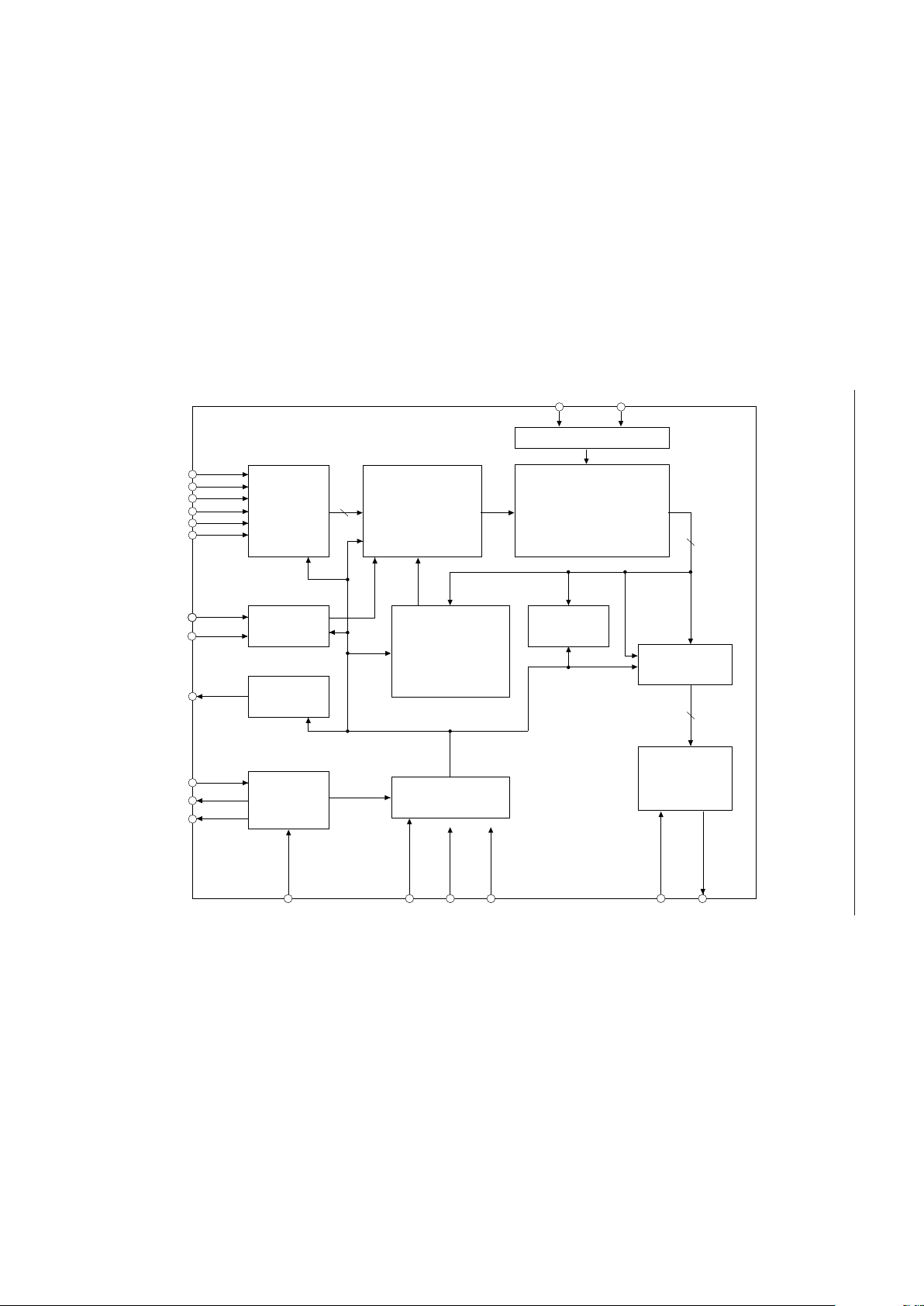
BLOCK DIAGRAM
2-Mbit OTP ROM
(Including 11 Kbits of
Edit ROM & Address ROM)
18-Bit
Multiplexer
Address &
Switching
Controller
6
PCM
Synthesizer
10
8
10-Bit
DAC
&
LPF
AOUT
DATA
Controller
18-Bit
Address Counter
Timing Controller
GNDV
DD
RESET
Random
Circuit
I/O
Interface
OSC
XT/RC
XT/CR
A2
A1
A0
SW2
SW1
SW0
RND
BUSY
OSC1
OSC2
OSC3/TEST
CPU/STD
V
REF
Program Circuit
V
PP
PGM

PIN CONFIGURATION (TOP VIEW)
MSM98P05¡ Semiconductor
V
PP
A0
A1
A2
RESET
XT/CR
BUSY
GND
V
REF
1
2
3
4
5
6
7
8
9
10 11AOUT V
20
PGM
19
SW2
18
SW1
17
SW0
16
RND
15
CPU/STD
14
OSC3/TEST
13
OSC2
12
OSC1
DD
20-Pin Plastic DIP
Note: Applies to MSM98P05RS
V
1
DD
NC
NC
RND
2
3
4
5
6
7
8
9
10
11
12
OSC1
OSC2
OSC3/TEST
CPU/STD XT/CR
PGM
SW0
SW1
SW2
24
23
22
21
20
19
18
17
16
15
14
13
NC: No connection
24-Pin Plastic SOP
AOUT
V
REF
GND
NC
BUSY
NC
RESET
V
PP
A2
A1
A0
Note: Applies to MSM98P05GS-K
3/13

PIN DESCRIPTIONS
MSM98P05¡ Semiconductor
DIP
5
7
6
15
9
10
8
11
12
13
14
16
Pin
SOP
17
20
18
7
23
24
22
1
2
3
5
8
Symbol Type Description
The IC enters the standby state if this pin is set to "L" level. At this time,
oscillation stops and AOUT drives a current of 0mA and becomes GND level,
RESET I
then the IC returns to the initial state. Apply a "L" pulse during power-on.
This pin has an internal pull-up resistor.
Outputs "L" level while voice is being played back.
BUSY O
In "H" level when power is turned ON.
XT/RC switching pin. Set to "H" level if ceramic oscillation is used. Set to "L"
XT/CR I
level if RC oscillation is used.
Microcontroller interface/stand-alone mode switching pin. Set to "L" level if
CPU/STD I
the IC is used in stand-alone mode.
Volume setting pin. If this pin is set to GND level, the maximum amplitude is
V
REF
I
This pin is internally connected to a pull-down resistor of approx. 10 kW
delivered. If this pin is set to V
level, the minimum amplitude is delivered.
DD
during IC operation.
Voice output pin.
AOUT O
The voice signals are output as current changes. A logic "L" is output from
this pin in standby state.
GND —
Ground pin.
Power supply pin. Insert a bypass capacitor of 0.1 mF or more between V
V
DD
—
and GND pins.
Ceramic oscillator connection pin when ceramic oscillation is selected.
OSC1 I
RC connection pin when RC oscillation is selected.
Input from this pin if external clock is used.
Ceramic oscillator connection pin when ceramic oscillation is selected.
RC connection pin when RC oscillation is selected.
OSC2 O
Leave this pin open if external clock is used.
Outputs "L" level in standby state.
Leave this pin open when ceramic oscillation is used.
OSC3/TEST O
RC connection pin when RC oscillation is selected.
Outputs "H" level in standby state when RC oscillation is selected.
Random playback starts if RND pin is set to "L" level.
Fetches addresses from random address generation circuit in the IC at the
RND I
falling edge of RND. Set to "H" level when the random playback function is
not used. This pin has internal pull-up resistor.
DD
4/13

MSM98P05¡ Semiconductor
DIP
17-19
2-4
1
20
Pin
SOP
10-12
13-15
16
9
Symbol Type Description
Phrase input pins corresponding to playback sound.
SW0 - SW2 I
A0 - A2 I
V
PP
PGM I
If input changes, SW0 to SW2 pins fetch addresses after 16 ms and start voice
synthesis. Each of these pins has internal pull-down resistor.
Phrase input pins corresponding to playback sound.
Logic input to A0 pin becomes invalid if the random playback function is used.
Power supply pin for writing to the built-in OTP. This pin should be set to "H"
—
level or be open during playback.
Interface pin for writing to the built-in OTP. This pin should be set to "L"
level or be open during playback.
5/13
 Loading...