E2D0082-29-93
¡ Semiconductor
This version: Sep. 1999
Previous version: May. 1997
MSM9836-xxx¡ Semiconductor
MSM9836-xxx
Voice Synthesis IC with Built-in Mask ROM
GENERAL DESCRIPTION
The MSM9836 is a PCM voice synthesis IC with built-in 3-Mbit mask ROM, D/A converter, and
low-pass filter (LPF).
The MSM9836 is specifically designed for applications that use a microcontroller.
For this reason, functional support for standalone mode and RC oscillation has been omitted
from the MSM9805, and the ROM capacity and the number of phrases have been increased.
By using Oki's Sound Analysis and Editing Tool, ROM data such as Phrase Control Table can be
easily set, created, edited, and evaluated.
The following table lists the functional differences between the MSM9836 and the MSM9805.
MSM9805
2 Mbits
Ceramic/RC
63
ROM Capacity
Interface
Oscillation
Maximum Number of
Phrases
Status Signal
MSM9836
3 Mbits
Microcontroller
Ceramic
127
NAR/BUSY simultaneous output
Microcontroller/Standalone
Only NAR output when operating
in microcontroller interface mode
FEATURES
• 8-bit OKI nonlinear PCM method/8-bit Straight PCM method
• Sampling frequency : 4.0 kHz/5.3 kHz/6.4 kHz/8.0 kHz/10.6 kHz/12.8 kHz/
(Can be set for each phrase) 16.0 kHz
• ROM capacity : 3 Mbits
• Maximum playback time : 97.7 sec (f
73.7 sec (f
61.0 sec (f
48.8 sec (f
• Master clock frequency : 4.096 MHz
(Ceramic oscillation/external
clock input)
• Edit ROM function
• Maximum number of phrases : 127
• Built-in current mode 10-bit D/A converter
• Built-in low-pass filter
• Power supply voltage : +2.0 to +5.5 V
• Package :
24-pin plastic SOP (SOP24-P-430-1.27-K) (Product name: MSM9836-xxxGS-K)
Chip
= 4.0 kHz)
SAM
= 5.3 kHz)
SAM
= 6.4 kHz)
SAM
= 8.0 kHz)
SAM
xxx indicates code number.
1/23

2/23
MSM9836-xxx¡ Semiconductor
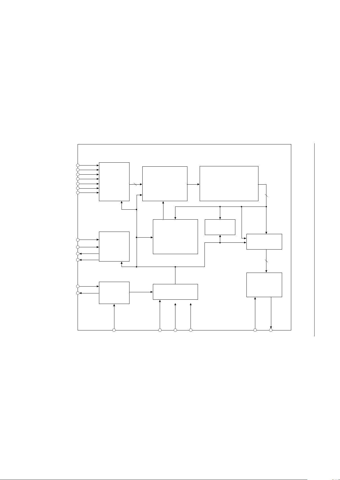
BLOCK DIAGRAM
3-Mbit ROM
(Including 17 Kbits of
Edit ROM & Address ROM)
19-Bit Multiplexer
Address
Controller
7
PCM
Synthesizer
10
8
10-Bit
DAC
&
LPF
AOUT
DATA
Controller
19-Bit
Address Counter
Timing Controller
GNDV
DD
RESET
I/O
Interface
Crystal
Circuit
EXTCK
I5
I4
I3
I2
I1
I0
ST
NAR
XT
XT
TEST
V
REF
I6
BUSY

PIN CONFIGURATION (TOP VIEW)
MSM9836-xxx¡ Semiconductor
V
1
DD
2
XT
3
XT
4
NC
ST
NC
I0
I1
I2
5
6
7
8
9
10
11
12
TEST
BUSY
EXTCK I6
24
23
22
21
20
19
18
17
16
15
14
13
AOUT
V
GND
NC
NAR
NC
RESET
NC
I5
I4
I3
NC : No connection
24-Pin Plastic SOP
REF
3/23

PIN DESCRIPTIONS
MSM9836-xxx¡ Semiconductor
Pin
17
20
7
23
24
22
1
2
3
5
8
10-15, 18
Symbol
RESET I
NAR O
EXTCK I
V
REF
AOUT O
GND —
V
DD
XT I
XT O
TEST I
ST I
BUSY O6
Type
I
—
Description
The IC enters the standby state if this pin is set to "L" level. At this time, oscillation
stops and AOUT output becomes GND level, then the IC returns to the initial state.
Apply a "L" pulse upon power-on.
This pin has an internal pull-up resistor.
Signal output pin that indicates whether the 7-bit LATCH (see Block Diagram) is idle.
NAR at "H" level indicates that the LATCH is empty and ST input is enabled.
Ceramic oscillator input/external clock input switching pin. Set to "H" level if ceramic
oscillation is used. Set to "L" level if external clock is used.
Volume setting pin. If this pin is set to GND level, the maximum current is forced in,
and if set to V
level, the minimum current is forced in.
DD
An approx. 10 kW pull-down resistor is internally connected to this pin during operation.
Voice output pin.
The voice signals are output as current changes. A "L" level signal is output through
this pin in standby state.
Ground pin.
Power supply pin. Insert a bypass capacitor of 0.1 mF or more between this pin and
the GND pin.
Ceramic oscillator connection pin when ceramic oscillation is selected.
Input from this pin if external clock is used.
Ceramic oscillator connection pin when ceramic oscillation is selected.
Leave this pin open if external clock is used.
A "L" level signal is output through this pin in standby state.
Normally leave this pin open. This pin is used only for testing the internal circuit.
Voice synthesis starts at fall of ST, and addresses I0 to I6 are fetched at rise of ST.
Input ST when NAR, the status signal, is at "H" level.
This pin has internal pull-up resistor.
Phrase input pins corresponding to playback sound.I0 - I6 I
This pin is at "H" level after reset is input. A "L" level signal is output through this pin
for the time during which voice is being played.
4/23

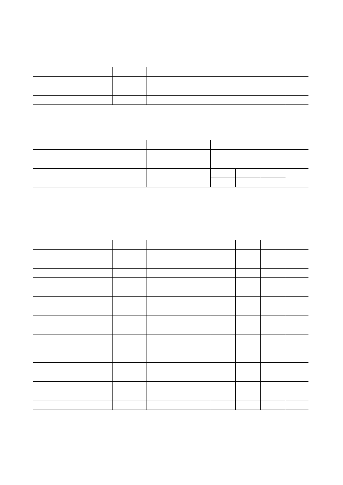
ABSOLUTE MAXIMUM RATINGS
Parameter Symbol Condition Rating Unit
Power Supply Voltage
Input Voltage
Storage Temperature
V
DD
V
IN
T
STG
Ta=25°C
RECOMMENDED OPERATING CONDITIONS
Parameter Symbol Condition Range Unit
Power Supply Voltage V
Operating Temperature —
Original Oscillation Frequency
T
f
DD
op
OSC
— 2.0 to 5.5 V
MSM9836-xxx¡ Semiconductor
–0.3 to +7.0 V
–0.3 to VDD + 0.3 V
–55 to +150 °C—
–40 to +85 °C
Min. Max.
Typ.
4.0963.5 4.5
(GND=0V)
(GND=0 V)
MHzWhen crystal is selected
ELECTRICAL CHARACTERISTICS
DC Characteristics (1)
(V
=5.0 V, GND=0 V, Ta=–40 to +85°C, unless otherwise specified)
DD
Parameter Symbol Condition Unit
"H" Input Voltage V
"L" Input Voltage —
Dynamic Supply Current 1 (*2)
Dynamic Supply Current 2 (*3)
Standby Current I
V
Pin Pull-Down Resistance
REF
IH
V
IL
V
OH
V
OL
IH1
Applies to XT pin only.
IH2
IL1
IL2
I
DD1
V
REF=VDD
At maximum output current
I
DD2
DS
=GND, AOUT voltage=0V
V
REF
At maximum output current
AOUT
R
VREF
V
REF=VDD
Min. Max.
——V
4.2 —
— 0.8
4.6 —
DD
V
IH=VDD
, AOUT voltage=0V
Typ.
—V
—V"H" Output Voltage IOH=–1 mA
—— 0.4
——10"H" Input Current 1 I
——15"H" Input Current 2 I
—–10 —"L" Input Current 1 I
–90–200 –30"L" Input Current 2 (*1) I
0.4—1
——16
——10
V"L" Output Voltage IOL=2 mA
µAVIH=V
µA
µAVIL=GND
µAInternal pull-up resistor
mA
mA
µATa=–40 to +70°C
——50µATa=–40 to +85°C
, AOUT voltage=0V
9.5615AOUT Output Current I
10713
mA
kW—
*1 Applicable to RESET, ST
*2 Dynamic supply current excluding DAC output current
*3 Dynamic supply current at maximum output current
5/23

DC Characteristics (2)
(V
=3.1 V, GND=0 V, Ta=–40 to +85°C, unless otherwise specified)
DD
Parameter Symbol Condition Unit
"H" Input Voltage V
"L" Input Voltage —
Dynamic Supply Current 1 (*2)
Dynamic Supply Current 2 (*3)
Standby Current I
V
Pin Pull-Down Resistance
REF
IH
V
IL
V
OH
V
OL
IH1
Applies to XT pin only.
IH2
IL1
IL2
I
DD1
V
REF=VDD
At maximum output current
I
DD2
DS
=GND, AOUT voltage=0V
V
REF
At maximum output current
AOUT
R
VREF
V
REF=VDD
MSM9836-xxx¡ Semiconductor
Min. Max.
——V
2.7 —
— 0.5
2.6 —
DD
V
IH=VDD
, AOUT voltage=0V
, AOUT voltage=0V
Typ.
—V
—V"H" Output Voltage IOH=–1 mA
—— 0.4
——10"H" Input Current 1 I
——15"H" Input Current 2 I
—–10 —"L" Input Current 1 I
–30–100 –10"L" Input Current 2 (*1) I
0.15— 0.5
—— 5.5
——5
V"L" Output Voltage IOL=2 mA
µAVIH=V
µA
µAVIL=GND
µAInternal pull-up resistor
mA
mA
µATa=–40 to +70°C
——20µATa=–40 to +85°C
3.21.4 5AOUT Output Current I
10713
mA
kW—
*1 Applicable to RESET, ST
*2 Dynamic supply current excluding DAC output current
*3 Dynamic supply current at maximum output current
6/23

AC Characteristics
Parameter Symbol Condition Unit
Master Clock Duty Cycle f
RESET Input Pulse Width —
RESET Input Time After Power-on
Standby Transition Time
(at end of voice output)
duty
t
w(RST)
t
D(RST)
STP
t
(ST)
t
SS
DW
WD
SNS
NAA
NAB
NAC
SBS
BSYA
, t
DAR
t
STB
BLN
Upon entering the stop code (*4)
SAM
SAM
SAM
SAM
SAM
SAM
DAF
SAM
MSM9836-xxx¡ Semiconductor
(V
=5.0 V, GND=0 V, f
DD
—50%
—
=8 kHz
=8 kHz
=8 kHz
=8 kHz
(*4)
(*4)
(*4)
=8 kHz
=8 kHz
(*4)
(*4)
(*4)
=8 kHz
(*4)
=4.096 MHz, Ta=–40 to +85°C)
OSC
Min. Max.
Typ.
40 60
10 —
0—
1
40
—µs
—µs
——t
—0.35 2000
——
—1—Data Setup Time t
—1—Data Hold Time t
——10NAR Output Time 1 t
375350 400NAR Output Time 2 t
440315 500NAR Output Time 3 t
375350 500NAR Output Time 4 t
——10BUSY Output Time 1 t
375350 400BUSY Output Time 2 t
6460 68D/A Converter Change Time t
250200 300
375350 500Silence Time Between Phrases t
µsST Signal Setup Time At power-on
µsST Input Pulse Width —
µsThe ST-ST Pulse Interval
µs—
µs—
µsf
µsf
µsf
µsf
µsf
µsf
ms—
ms—
µsf
*4 Proportional to master the periods of oscillation frequency f
OSC1
and f
OSC2
.
The rated values show values when the standard master oscillation frequency is used.
7/23

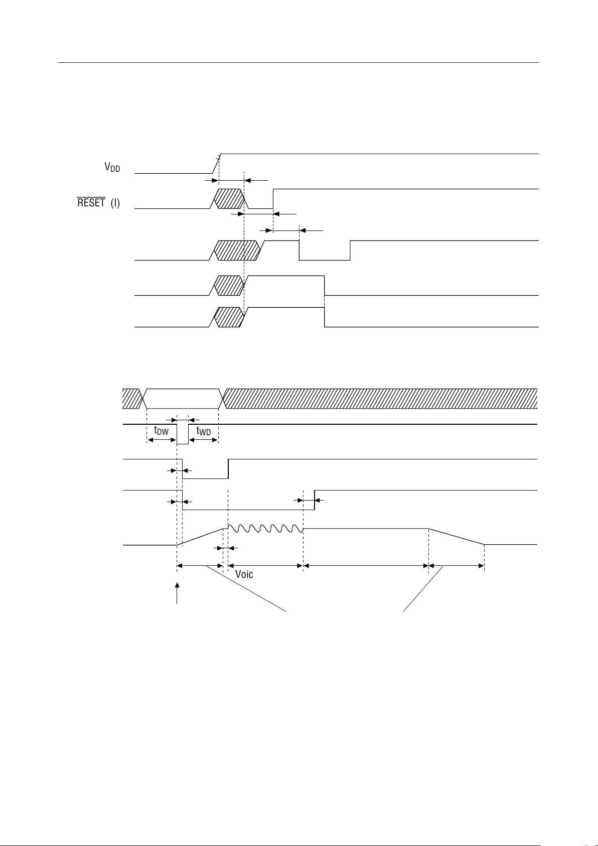
TIMING DIAGRAMS
1. AC Characteristics at Power-On
V
Min
V
DD
RESET (I)
ST (I)
NAR (O)
BUSY (O)
DD
t
D(RST)
t
W(RST)
t
MSM9836-xxx¡ Semiconductor
STP
2. AC Characteristics in Standby Status and when the IC is Activated
I6 to I0 (I)
t
(ST)
ST (
I
NAR (O)
BUSY (O)
AOUT (O)
t
)
DW
Oscillation start
t
DAR
t
t
SNS
t
WD
SBS
t
NAA
Voice playback
t
BSYA
t
STB
Standby transtion time
D/A converter change time
t
DAF
8/23
 Loading...