OKI MSM9810GS-BK Datasheet

E2D0020-39-93
¡ Semiconductor MSM9810
¡ Semiconductor
This version: Sep. 1999
Previous version: May 1997
MSM9810
8-channel Mixing OKI ADPCM Type Voice Synthesis LSI
GENERAL DESCRIPTION
The MSM9810 is an 8-channel mixing voice synthesis IC, to which up to 128 Mbits of ROM and/
or EPROM storing voice data can directly be connected externally.
The device is straight 8-bit PCM playback, non-linear 8-bit PCM playback, 4-bit ADPCM
playback, and 4-bit ADPCM2 playback selectable and provides 2-channel stereo output and
volume control. The MSM9810 contains a 14-bit D/A converter and LPF.
The MSM9810 can easily configure a system by connecting voice data storage memory, power
amplifier, and CPU externally.
FEATURES
• Non-linear 8-bit PCM / straight 8-bit PCM / 4-bit ADPCM / 4-bit ADPCM2
• Serial input or parallel input selectable
• Phrase Control Table function
• 8-channel mixing function
• Master clock frequency : 4.096 MHz
• Sampling frequency : 4.0 kHz, 5.3 kHz, 6.4 kHz, 8.0 kHz, 10.6 kHz,
12.8 kHz, 16.0 kHz, 21.2 kHz, 25.6kHz, 32.0kHz
• Maximum number of phrases : 256
• Output channel : L/R 2 channels
• Built-in volume control function (for each output channel)
• Built-in 14-bit D/A converter
• Built–in low–pass filter : Digital filter
• Package :
64-pin plastic QFP(QFP64-P-1414-0.80-BK)(Product name : MSM9810GS-BK)
New
1/31
RA23 RA0
ROE
RD7
RD0
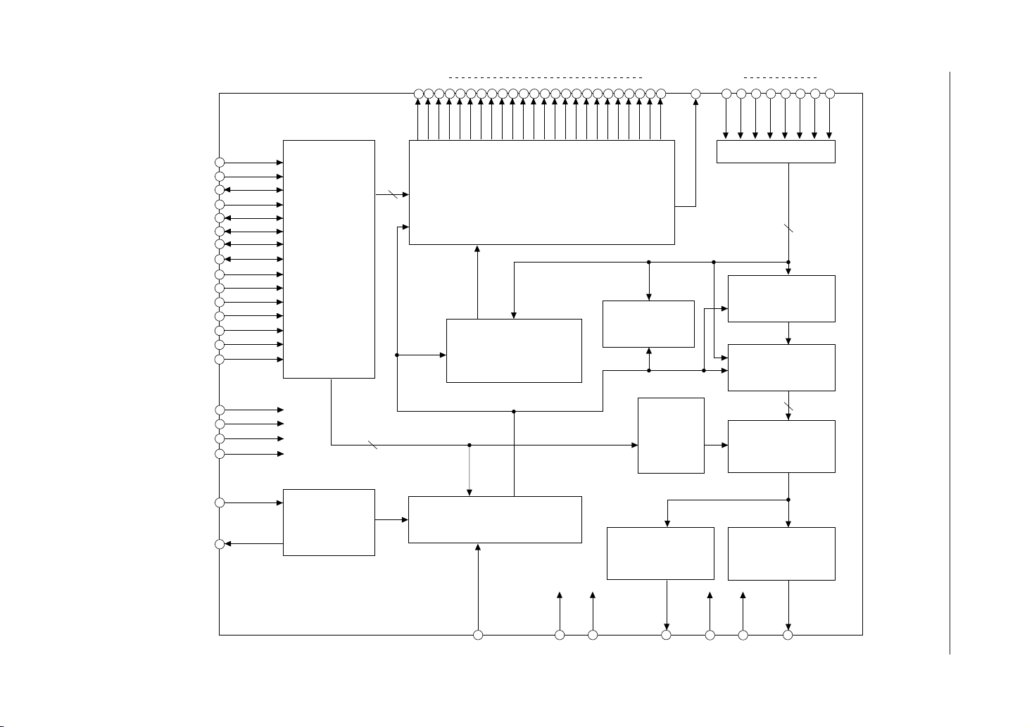
BLOCK DIAGRAM
¡ Semiconductor MSM9810
D7/SD
D6/SI
D5/SO
D4/UD
D3/SR3
D2/SR2
D1/SR1
D0/SR0
RCS
CS
WR
RD
CMD
SERIAL
NCR/BUSY
TEST1
TEST2
TEST3
TEST4
XT
XT
CPU
interface
OSC
8-Bit LATCH
8
23-Bit Multiplexer
8
ADPCM
DATA
Synthesizer
Controller
23-Bit Address
Counter
PCM
Synthesizer
16
8
PAN
Register
16*9 MPY
Timing Controller
14-Bit
DAC
14-Bit
DAC
2/31
RESET
DD
DGNDDV
LDAO
DD
AGNDAV
RDAO

¡ Semiconductor MSM9810
PIN CONFIGURATION (TOP VIEW)
RA23
RA22
RA21
RA20
RA0
RA17
RA16
RA15
RA14
RA13
RA12
DGND
AGND
TEST4
LDAO
RDAO
AV
DD
DV
DD
RCS
TEST1
TEST2
XT
6463626160595857565554
1
2
3
4
5
6
7
8
9
10
11
12XT
13TEST3
14SERIAL
15CMD
16RD
53 RA11
52 RA10
51 RA9
50 RA19
49 RA18
48
DV
RA8
47
RA7
46
RA6
45
RA5
44
RA4
43
RA3
42
RA2
41
RA1
40
ROE
39
RD0
38
37 RD1
36 RD2
35 RD3
34 RD4
33 RD5
DD
1718192021222324252627
WR
NCR/BUSY
CS
D0/SR0
D1/SR1
D2/SR2
D3/SR3
D5/SO
D4/UD
D6/SI
NC
NC: No connection
64-pin Plastic QFP
28D7/SD
29RESET
30RD7
31RD6
32DGND
3/31

¡ Semiconductor MSM9810
PIN DESCRIPTIONS
Pin
40-47, 49-64
30, 31, 33-38
39
8
15
16
18
20
14
28
27
26
Symbol Type
RA23-RA0 O
RD7-RD0 I
ROE O Output enable pin for external memory.
RCS I
CMD I
RD I
WR I
CS I
SERIAL I
D7/SD I/O
D6/SI I/O
D5/SO I/O
Address pins for external memory. These pins become high impedance
when RCS pin is "H".
Data pin for external memory. Pull-down resistors are internally
connected to these pins. These pull-down resistors become valid when
the RCS pin is "H", and become invalid when the RCS pin is "L".
When this pin is "L", RA23 to RA0 and ROE pins output address data and
output enable signal.
When this pin is "H", RA23 to RA0 and ROE pins become high impedance.
Select pin for Command data or Subcommand data.
When this pin is "H", subcommand input is selected. When this pin is "L",
command input is selected.
A pull-up resistor is internally connected to this pin.
Read pin for CPU interface.
A pull-up resistor is internally connected to this pin.
Write pin for CPU interface.
A pull-up resistor is internally connected to this pin.
Chip select pin for CPU interface. When CS is "H", WR signal is not
entered in this IC. A pull-up resistor is internally connected to this pin.
CPU interface select pin. When SERIAL is "H", serial input interface is
selected.
When it is "L", parallel input interface is selected.
Data bus pin for CPU interface when parallel input interface is selected.
When WR is "L", this pin serves as data input pin.
When RD is "L", this pin serves as channel status data output pin.
When serial input interface is selected, this pin serves as serial data
input pin.
Data bus pin for CPU interface when parallel input interface is selected.
When WR is "L", this pin serves as data input pin.
When RD is "L", this pin serves as channel status output pin.
When serial input interface is selected, this pin serves as serial clock
input pin.
Data bus pin for CPU interface when parallel input interface is selected.
When WR is "L", this pin serves as data input pin.
When RD is "L", this pin serves as channel status output pin.
When serial input interface is selected, this pin serves as channel status
output pin.
Description
4/31

¡ Semiconductor MSM9810
Symbol Type DescriptionPin
Data bus pin for CPU interface when parallel input interface is selected.
When WR is "L", this pin serves as data input pin.
When RD is "L", this pin serves as channel status output pin.
25
24
23
22
21
4
5
11
12
29
19
9
10
13
3
7, 48
6
1, 32
2
D4/UD I/O
D3/SR3
D2/SR2
D1/SR1
D0/SR0
LDA0 O LEFT side D/A output pin.
RDA0 O RIGHT side D/A output pin.
XT I
XT O
RESET I
NCR/BUSY I
TEST1
TEST2
TEST3
TEST4
DV
DD
AV
DD
DGND
AGND
When serial input interface is selected, this pin serves as channel status
selecter pin.
When UD is "H", channels 8 thru 5 are output to SR3 thru SR0, respectively.
When UD is "L", channels 4 thru 1 are output to SR3 thru SR0, respectively.
Data bus pin for CPU interface when parallel input interface is selected.
When WR is "L", this pin serves as data input pin.
When RD is "L", this pin serves as channel status output pin.
When serial input interface is selected, this pin serves as channel status
I/O
output pin.
When UD is "H", channels 8 thru 5 are output to SR3 thru SR0, respectively.
When UD is "L", channels 4 thru 1 are output to SR3 thru SR0, respectively.
Crystal or ceramic oscillator connection pin.
A feedback resistor of about 1MW is connected between XT and XT.
If necessary, enter external clocks into this pin.
Crystal or ceramic oscillator connection pin.
When external clocks are used, leave this pin open.
When this pin is "L" level, the LSI is initialized. At that time, oscillation
stopsand D/A outputs go to GND level.
Channel status select pin.
When this pin is "H", NCR signal is output. When it is "L", BUSY signal is
output.
Pins for IC testing. Apply "L" level to these pins.
Pull-down resistors are internally connected to these pins.
I
I Pins for IC testing. Apply "L" level to these pins.
Power supply pin.
—
GND pin.
—
5/31
¡ Semiconductor MSM9810
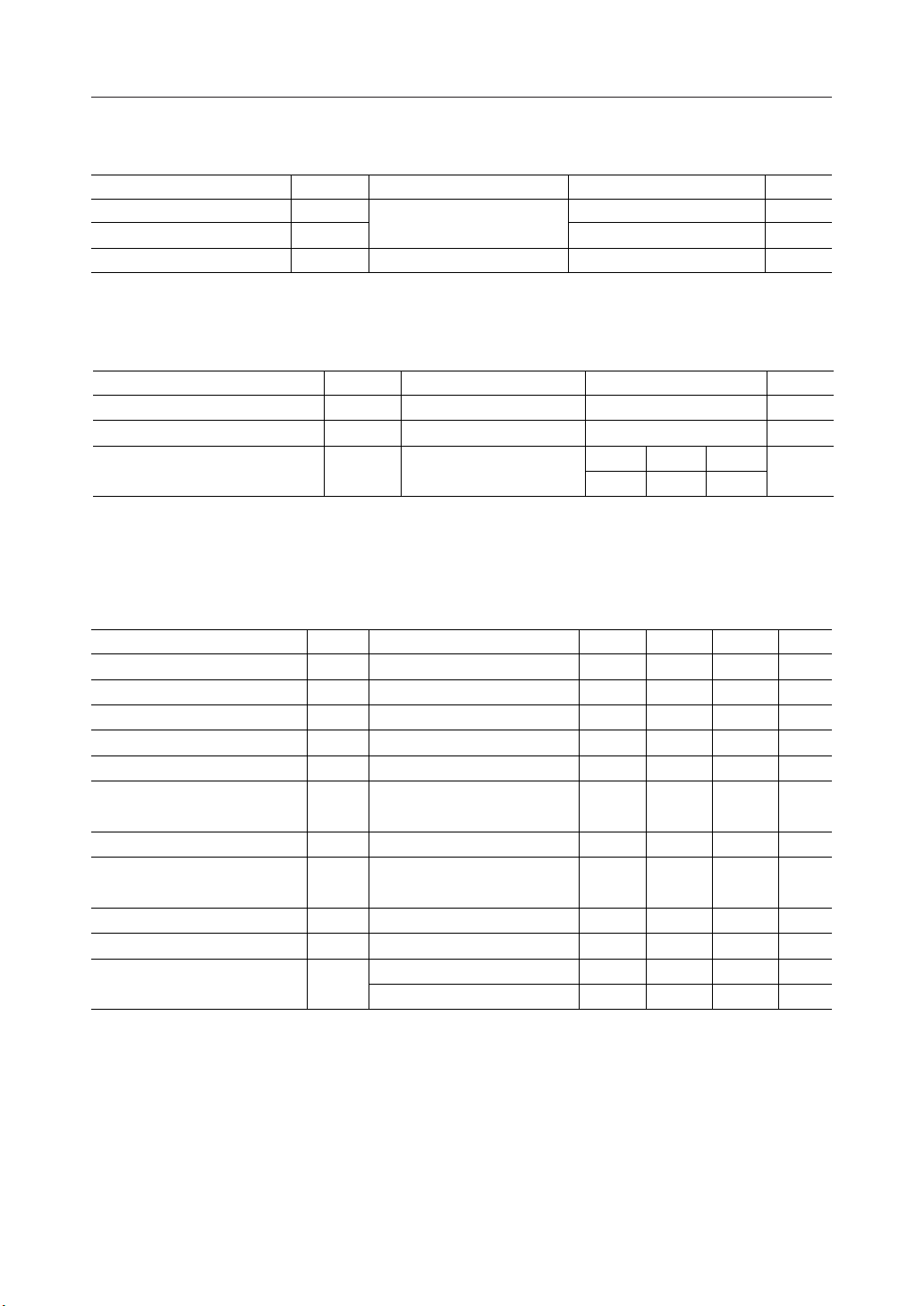
ABSOLUTE MAXIMUM RATINGS
Parameter Symbol Condition Rating Unit
Power Supply Voltage
Input Voltage
Storage Temperature
V
DD
V
IN
T
STG
Ta=25°C
—
RECOMMENDED OPERATING CONDITIONS
Parameter Symbol Condition Range Unit
Power Supply Voltage
Operating Temperature
Master Clock Frequency
V
T
f
OSC
DD
op
— 3.5 to 5.5 V
— –40 to +85 °C
—
ELECTRICAL CHARACTERISTICS
DC Characteristics
(DVDD=AVDD=4.5 to 5.5 V, DGND=AGND=0 V, Ta=–40 to +85°C)
Parameter Symbol Condition Min. Unit
High-level Input Voltage V
Low-level Input Voltage V
High-level Output Voltage V
Low-level Output Voltage V
High-level Input Current 1 I
High-level Input Current 2 I
Low-level Input Current 1 I
Low-level Input Current 2 I
Output Leakage Current I
Operating Current I
Standby Current I
IH1
IH2
IL1
IL2
LO
DD
DS
IH
IL
OH
OL
Applied to pins with internal
Applied to pins with internal
Ta = –40°C to +70°C — mA—15
Ta
— 0.84¥V
—— V— 0.16¥V
I
= –1mA VDD–0.4 V——
OH
I
= 2mA — V— 0.4
OL
V
= V
IH
DD
pull-down resistor
V
= GND –10 mA——
IL
pull-up resistor
0 £ V
OUT
£ V
—— mA615
= –40°C to +85°C — mA—50
DD
(GND=0 V)
–0.3 to +7.0
–0.3 to V
DD
+0.3
–55 to +150
(GND=0 V)
Min. Max.
3.5 4.5
Typ.
4.096
Typ. Max.
DD
DD
— mA—10
30 mA— 300
–300 mA— –30
–10 mA— +10
V
V
°C
MHz
V——
6/31

¡ Semiconductor MSM9810
AC Characteristics
(VDD=3.5 to 5.5V, GND=0 V, Ta=–40 to +85°C)
Parameter Symbol Min. Unit
Master Clock Duty Cycle
RESET Input Pulse Width
RESET Delay Time From Raising of Power Supply
Set up and Hold Time of CS for RD, at serial input I/F
RD Pulse Width
Output Data Valid Time after Fall of RD
Data Float Time after Rise of RD
Setup and Hold Time of CMD for WR
Setup and Hold Time of CS for WR
WR Pulse Width
Data Setup Time before Rise of WR
Data Hold Time after Rise of WR
WR-WR Pulse Interval
CS-CS Pulse Interval
Serial Data Setup Time
Serial Data Hold Time
Serial Clock Pulse Width
fduty
tw(RST)
tD(RST)
tCR
tRR
tDRE
tDRF
tDW
tCW
tWW
tDWS
tDWH
tWWS
tCC
tSDS
tSSD
tW(SCK)
40
1
0
30
200
—
—
50
30
200
100
30
160
100
30
30
200
Typ. Max.
50
—
—
—
—
—
10
—
—
—
—
—
—
—
—
—
—
60
—
—
—
—
100
50
—
—
—
—
—
—
—
—
—
—
%
ms
ms
ns
ns
ns
ns
ns
ns
ns
ns
ns
ns
ns
ns
ns
ns
7/31
¡ Semiconductor MSM9810
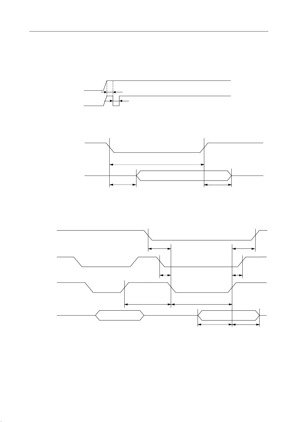
TIMING DIAGRAMS
Power-On Timing
V
DD
RESET (I)
Data Read Timing, Parallel Input
RD(I)
t
D(RST)
t
W(RST)
t
RR
D7 - D0(I/O)
Data Write Timing, Parallel Input
CMD(I)
CS(I)
WR(I)
D7 - D0(I)
Data Stable
t
DRE
t
WSS
Data out Valid
t
DW
t
CW
t
WW
t
DRF
Data Stable
t
DWS
t
DW
t
CW
t
DWH
8/31
¡ Semiconductor MSM9810
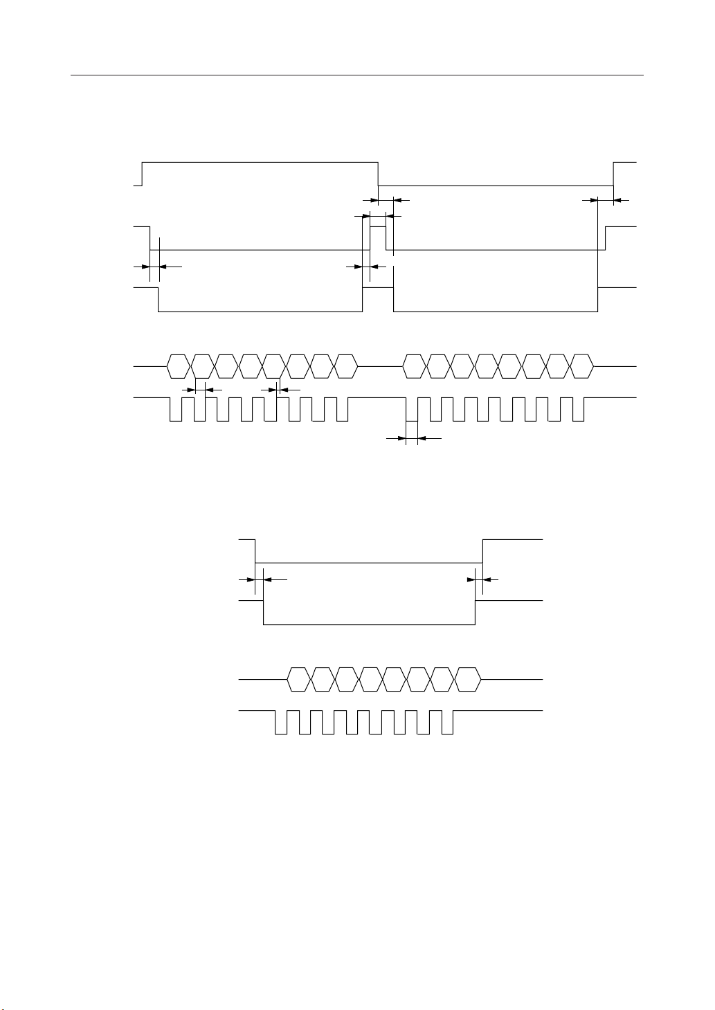
Data Write Timing, Serial Input
CMD(I)
CS(I)
WR(I)
SD(I)
SI(I)
t
DW
t
CC
t
CW
t
SDS
t
SSD
t
CW
t
W(SCK)
t
DW
Data Read Timing, Serial Input
CS(I)
RD(I)
SO(I)
SI(I)
t
CR
t
CR
9/31
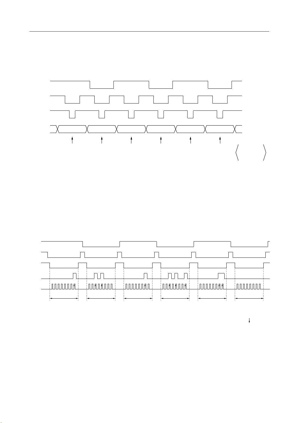
¡ Semiconductor MSM9810
Command input timing in parallel input interface
• The phrase address "25H" data is played back via channel 1
• The command options selected are 1/2 V
(P-P) sound volume for all channels, use of an
DD
internal low pass filter, secondary digital filter processing, and voltage follower output.
CMD
CS
WR
D7-D0
09H 18H 25H 28H 01H 00H
Set option data
Subcommand
(OPT)
Transfer option
data Command
(OPT)
Set address
data Subcommand
(FADR)
Transfer address
data to channel 1
Command
(FADR)
Set Start flag
to channel 1
Subcommand
(START)
Start flag execution
(Channel 1)
Command
(START)
Channel 1 voice
systhesis starts
See 9. "Command Data and Subcommand Data" for further information on commands and subcommands.
Command input timing in serial input interface
• Phrase address "08H" to channel 1 data and Phrase address "02H" to channel 2 data are played
back simultaneously.
• The command option is default setting.
CMD
CS
WR
SD
SI
(08H)
Set address "01H" data
Subcommand
(FADR)
See 3-1 "Channel Synthesis" for further information on channel synthesis.
(28H)
Transfer address
data to channel 1
Command
(FADR)
(02H)
Set address "02H" data
Subcommand
(FADR)
(29H)
Transfer address data
to channel 2
(FADR)
(03H)
Set start flag to channel 1
and channel 2
Subcommand
(START)
(00H)
Start flag execution
(channel 1 and channel 2)
Command (START)
Channel 1 and channel 2
voice synthesis starts
10/31
 Loading...