

OKI MSM9405MB Datasheet

E2F0007-18-11
Preliminary
This version: Jan. 1998
MSM9405¡ Semiconductor
¡ Semiconductor
MSM9405
IrDA Communication Controller
GENERAL DESCRIPTION
The MSM9405 is a communication controller conforming to IrDA, the international standard for
infrared data communication. The device covers the IrDA physical specifications Ver.1.0 and
1.1.
Since the device performs some of the functions concerning communication protocol control,
the load on the software (firmware) for protocol control can be reduced. By combining the
device with another microcontroller and an infrared transceiver module, a device provided
with IrDA-compliant communication function can be configured.
FEATURES
• Data transfer rates
IrDA 1.0 : 2400, 9600 bps; 19.2, 38.4, 57.6, 115.2 kbps
IrDA 1.1 : 0.576, 1.152, 4 Mbps
• Detection/removal for beginning of frame and end of frame (IrDA 1.0, 1.1)
Insertion for beginning of frame and end of frame (IrDA 1.0, 1.1)
• Generation/check for CRC (IrDA 1.0, 1.1)
• Host interface
8-bit data bus : D0-D
DMA transfer : DREQ, DACK, TC
Interrupt : INTR
Address : A0-A
Control signal : CS, RD, WR
• Infrared module control signal : SD
• Built-in 32-byte transmit-receive FIFOs
• Power down mode
• Built-in oscillator circuit
7
3
• Crystal oscillation frequency : 18.432 MHz (other than 4 Mbps data rate)
: 48 MHz (when 4 Mbps data rate used)
• Operating voltage (VDD) : 2.7 to 3.6 V
• Package:
30-pin plastic SSOP (SSOP30-P-56-0.65-K) (Product name : MSM9405MB)
1/30
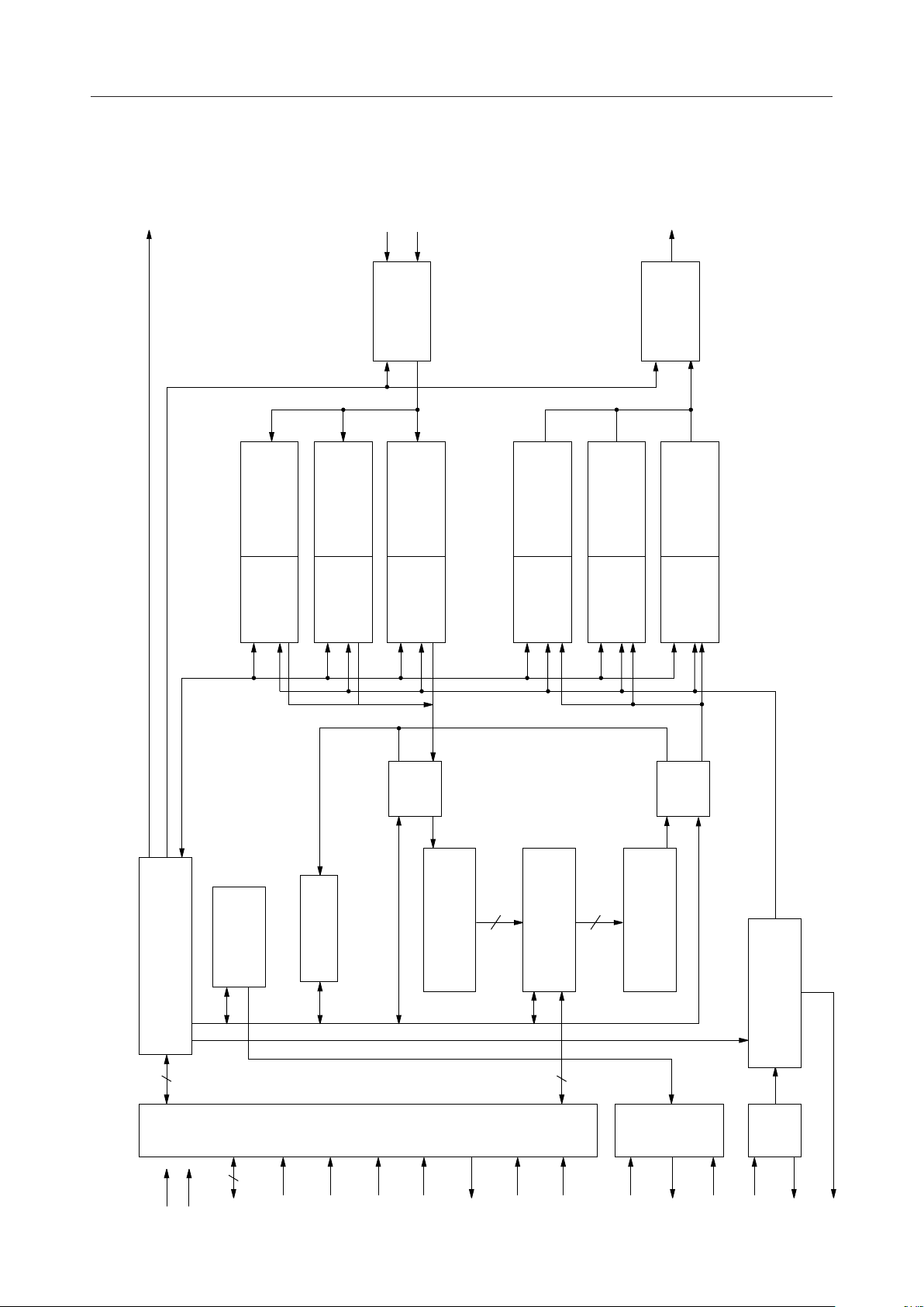
BLOCK DIAGRAM
SD
IRIN-A
IRIN-B
MSM9405¡ Semiconductor
IROUT
DEC
UART
Flag Detection/
Removal Circuit
IrDA
Flag Detection/
Removal Circuit
DEC
HDLC-
Demodulator
Removal Circuit
Preamble/Flag Detection/
DEC
4 PPM-
ENC
UART
Circuit
Flag Insertion
IrDA
Modulator
Flag Insertion Circuit
ENC
HDLC-
Preamble/Flag/
4 PPM-
Insertion Circuit
ENC
Register
Control/Status
8
DD
V
GND
DMA
Control Circuit
8
0-7
D
TCC/RCC
Microcontroller I/F
0-3
A
CS
RD
RX_
CRC
WR
Receive Shift
Register (RSR)
INTR
8
(32¥8bit)
Transmit-Receive FIFO
8
PWDN
RESET
8
(TSR)
Transmit Shift Register
DMA
TC
TX_
I/F
DREQ
CRC
DACK
Generator
Baud Rate
OSC
XIN
XOUT
TEST
2/30
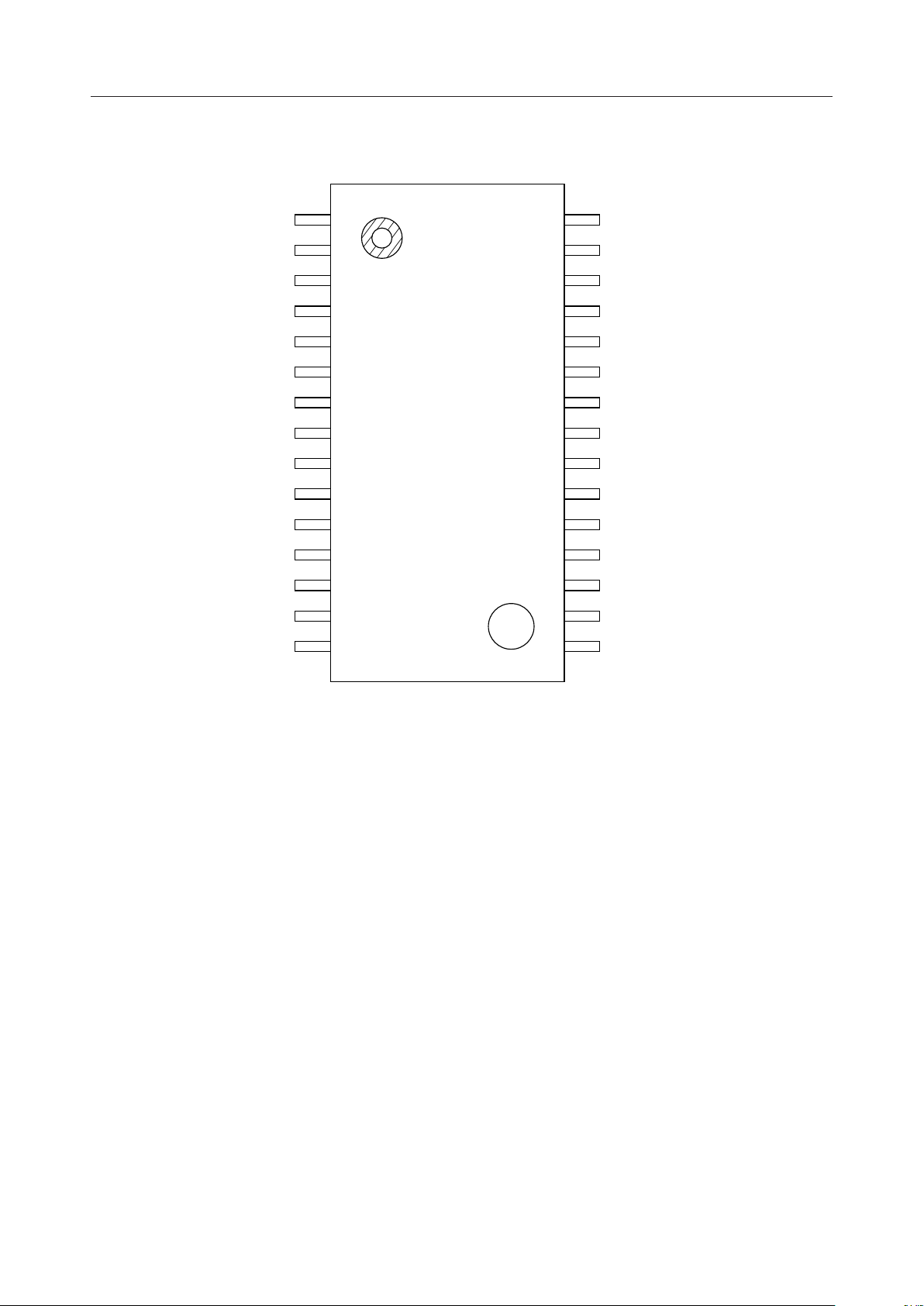
PIN CONFIGURATION (TOP VIEW)
MSM9405¡ Semiconductor
V
DD
D
D
D
D
D
D
D
D
A
A
A
A
CS
RD
1
2
7
3
6
4
5
5
4
6
3
7
2
8
1
9
0
10
3
11
2
12
1
13
0
14
15
30
XIN
29
XOUT
28
TEST
27
IRIN-A
26
IRIN-B
25
IROUT
24
SD
23
TC
22
DREQ
21
DACK
20
PWDN
19
RESET
18
INTR
17
WR
16
GND
30-Pin Plastic SSOP
3/30
PIN DESCRIPTIONS
MSM9405¡ Semiconductor
Transceiver
Module Interface
Microcontroller
Interface
DMA Controller
Interface
Others
27
26
25
9-2
13-10
14
15
17
18
22
21
23
20
19
Type
IRIN-A I
IRIN-B I
IROUT O
SD O24
D0-D
A0-A
I/O
7
3
CS
RD I
WR I
INTR O
DREQ O
DACK
TC I
PWDN I
RESET I
DescriptionSymbolPinFunction
Receive signal input A. (2.4 kbps to 4 Mbps)
*1
Receive signal input B. (0.576 to 4 Mbps)
When connecting this device to a transceiver module,
tie this pin high or low if the number of the receive signal
output pins that the module has is only one.
*1
Transmit signal output. Active high.
Transceiver module control signal output.
Becomes active when PWDN is set low.
*1
This pin must be left open if connecting this device to a
transceiver module having no shutdown pins.
Data input-output.
I
Register address inputs.
I
Chip select input. Active low.
When low, read and write signals are enabled.
Read signal input. Active low.
Write signal input. Active low.
Interrupt request signal output. Active low.
DMA Request signal output.
I
DMA acknowledge signal input.
*1
*1
DMA transfer end signal input. Active low.
Power down control. Active low.
When set low, oscillation stops and the device enters power
down (low supply current) mode.
System reset input. Active low.
When set low, the internal registers are initialized.
28
30
29
1
16
TEST O
XIN I
XOUT O
V
DD
—
GND —
Test. Must be left open.
Crystal connect.
Crystal connect.
Power supply.
Ground.
*1 Either active high or active low can be selected depending on the register setting.
4/30
ABSOLUTE MAXIMUM RATINGS
Parameter Symbol Condition Rating Unit
Supply Voltage V
Input Voltage V
Power Dissipation P
Storage Temperature T
DD
I
D
STG
— –0.5 to +4.0 V
— –0.5 to +6.0 V
— 230 mW
— –55 to +150 °C
RECOMMENDED OPERATING CONDITIONS
Parameter Symbol Condition Range Unit
Supply Voltage V
Operating Temperature T
Crystal Oscillation
Frequency
f
OSC
DD
op
— 2.7 to 3.6 V
— –20 to +70 °C
— 18.432 MHz ±200 ppm or 48 MHz ±100 ppm —
MSM9405¡ Semiconductor
ELECTRICAL CHARACTERISTICS
DC Characteristics
= 2.7 to 3.6 V, Ta = –20 to +70°C)
(V
DD
Parameter Symbol Condition Applicable Pin
"H" Input Voltage V
"L" Input Voltage V
Input Leakage Current I
"H" Input Voltage V
"L" Input Voltage V
Input Leakage Current I
"H" Output Voltage V
"L" Output Voltage V
"H" Output Voltage V
"L" Output Voltage V
Supply Current I
IH
IL
LI
IH
IL
LI
OH
OL
OH
OL
DD
— IRIN-A, IRIN-B, PWDN
—A
VI = VDD/0 V TC, RESET, DACK
—
—
VI = VDD/0 V
IO = –4 mA
IO = 4 mA — — 0.4
IO = –4 mA 2.4 — —
IO = 4 mA — — 0.4
———20 V
Supply Current
(during Power Down)
I
DPN
When PWDN = "L" — — — V
Min.
2.2
0
—
2.2
0
—
2.4
Typ.
—
—
—
—
—
—
—
Max.
5.5
*1
0.8
±1
5.5
*1
0.8
±10—mA
Unit
V
mA
V
V
V
mA
mA
0-A3
IROUT, INTR, DREQ
, CS, RD, WR,
D
0-D7
DD
DD
*1 1.0 V when V
= 3.0 to 3.6 V
DD
5/30

AC Characteristics
Parameter Symbol Condition Note
Read Pulse Width t
Read Data Delay Time t
Read Data Hold Time t
Read/Write Recovery Time t
CS Setup Time t
CS Hold Time t
Write Address Hold Time t
Write Pulse Width t
Write Data Setup Time t
Write Data Hold Time t
Write Address Setup Time t
Interrupt Clear Time t
DACK Pulse Width t
DACK Setup Time t
DREQ Clear Time t
DACK Hold Time (during Read) t
DACK Hold Time (during Write) t
TC Pulse Width t
TC Setup Time t
TC Hold Time t
SIR Pulse Width t
SIR Data Rate Tolerance SDRT
MIR Pulse width t
MIR Data Rate Tolerance MDRT
FIR Single Pulse Width t
FIR Data Rate Tolerance FDRT
FIR Double Pulse Width t
Reset Pulse Width t
rpw
rdd
rdh
rcv
css
csh
wah
wpw
wds
wdh
was
intr
dak
acs
drqr
achr
achw
tcw
tcs
tch
spw
mpw
fpw
fdpw
rstw
= 2.7 to 3.6 V, Ta = –20 to +70°C)
(V
DD
Min.
—
— *2
— *3
120/70
—
0
Typ.
—
—
—
Max.
—
60
20
Unit
ns
ns
ns
—ns——60
—ns——60
—ns——0
—ns——0
—ns——120/70
—ns——60
—ns——–10
—ns——–10
—ns120/70——
—ns——60
—ns——10
—ns120/70——
—ns——–5
—ns——10
—ns——50
—ns——0
—ns——0
Transmitter ms—1.63—
Receiver ms——0.9
Transmitter %±0.87——
Receiver %±2.0——
Transmitter ns—218—
Receiver ns——100
Transmitter %±0.1——
Receiver %±0.2——
Transmitter ns—125—
Receiver ns165—70
Transmitter %±0.01——
Receiver %±0.1——
Transmitter ns—250—
Receiver ns285—195
—ns——70
MSM9405¡ Semiconductor
*1
*1
*1
*1
*1 120 ns when crystal oscillation frequency = 18.432 MHz,
70 ns when crystal oscillation frequency = 48 MHz
*2 That which occurs latest of the following is to be used for the data delay time (t
the change of the state of A0-A3, the change from CS high to low, and the change from
RD high to low.
*3 That which occurs first of the following is to be used for the read data hold time (t
the change of the state of A0-A3, the change from CS low to high, and the change from
RD low to high.
rdd
rdh
6/30
) :
) :

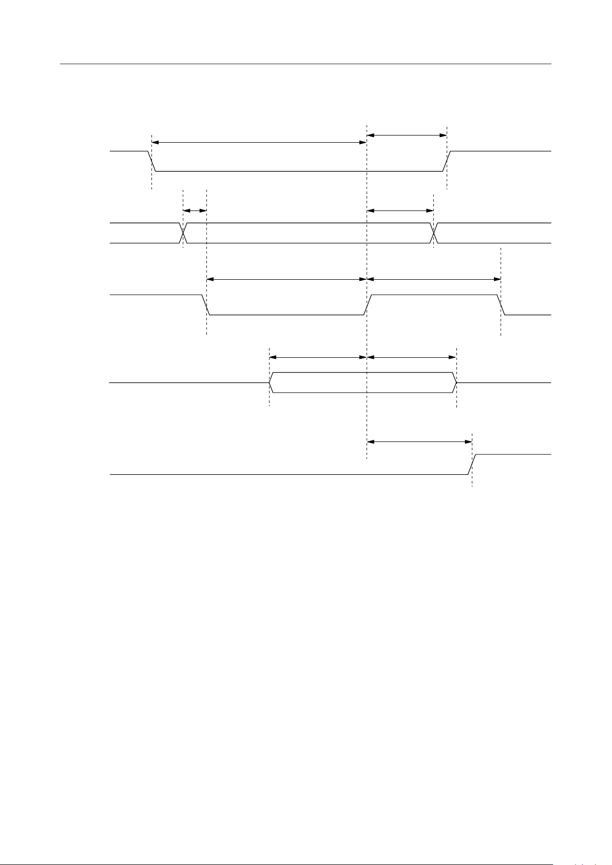
• Read timing
MSM9405¡ Semiconductor
t
rdd
CS
A
RD
D
0-A3
-D
0
t
rpw
t
rdd
t
rpw
t
rpw
t
rdd
7
t
rdh
t
rdh
t
rdh
t
rcv
INTR
t
intr
7/30
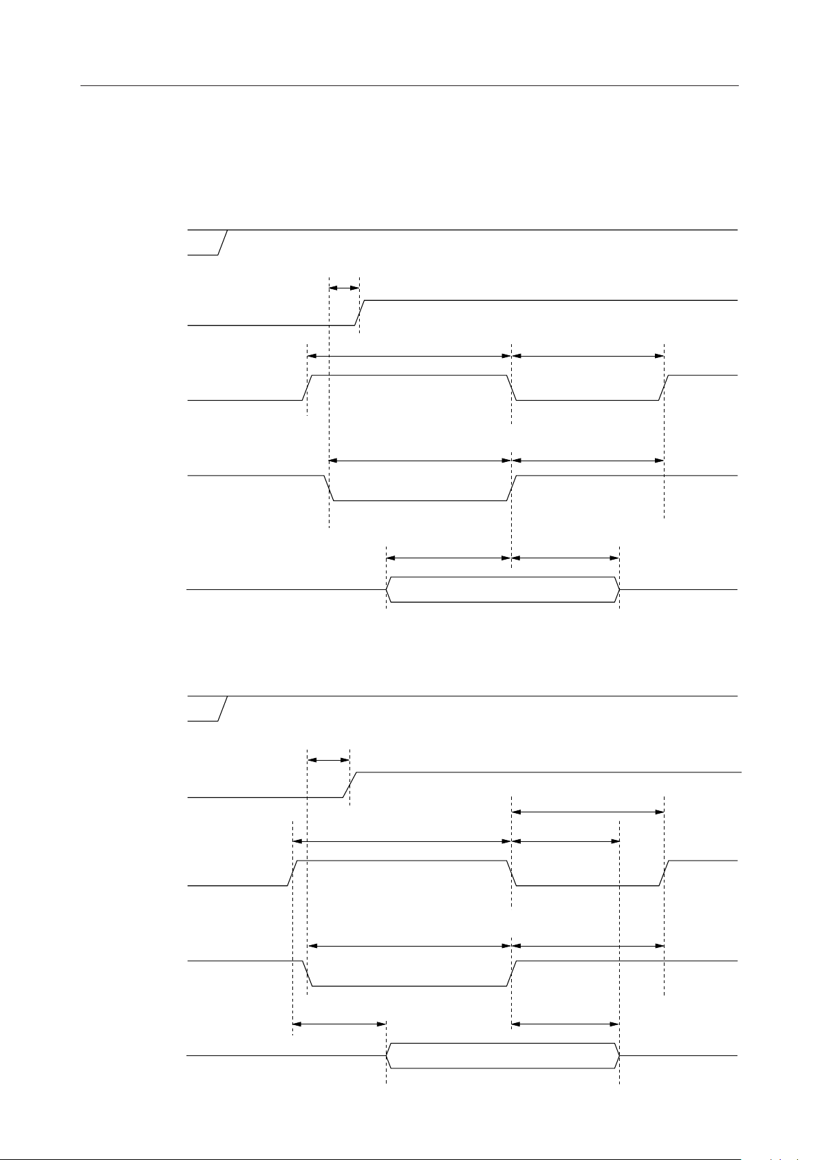
• Write timing
CS
t
css
t
MSM9405¡ Semiconductor
csh
A
0-A3
WR
D
0-D7
INTR
t
was
t
wpw
t
wds
t
wah
t
wdh
t
intr
t
rcv
8/30
• DMAC access timing 1
DMA_EN = "1", DMA_SL1 = "0", DMA_SL0 = "0"
MemoryÆM9405
CS
DREQ
(Active low)
DACK
t
drqr
MSM9405¡ Semiconductor
t
dak
t
rcv
RD
D
0-D7
M9405ÆMemory
CS
DREQ
(Active low)
t
drqr
t
t
rpw
dak
t
wds
t
wdh
t
rdh
t
rcv
t
rcv
DACK
WR
D
0-D7
t
wpw
t
rdd
t
rcv
t
rdh
9/30
 Loading...