

OKI MSM9225GS-2K Datasheet

E2F0016-19-43
This version: Aug. 1998
¡ Semiconductor
This version: Apr. 1999
MSM9225
¡ Semiconductor
MSM9225
CAN (Controller Area Network) Controller
GENERAL DESCRIPTION
The MSM9225 is a microcontroller peripheral LSI which conforms to the CAN protocol for
high-speed LANs in automobiles.
FEATURES
•Conforms to CAN protocol specification (Bosch Co., V.2.0 part b/Full CAN)
• Maximum 1 Mbps real-time communication control (programmable)
• Communication system:
Transmission line is bi-directional, two-wire serial communications
NRZ (Non-Return to Zero) system using bit stuff function
Multi-master system
Broadcast system
• Maximum 16 messages ¥ 8 bytes of message buffer
Number of messages can be extended by group message function (max: 2 groups)
• Priority control by identifier
Normally 2032 types, 2032 ¥ 218 types at extension
• Microcontroller interface
Corresponding to both parallel and serial interface
Parallel interface: separate address/data bus type (with address latch signal/no
address latch signal) and multiplexed address/data bus type.
Serial interface: Synchronous communication type
Interrupt is used for three outputs: transmission/receive/error
• Error control:
Bit error/stuff error/CRC error/form error/acknowledge error detection functions
Retransmission / error status monitoring function when error occurs
• Communication control by transmission request function
• Sleep/Stop mode function
• Supply voltage: 5 V ±10%
• Operating temperature: -40 to +115˚C
• Package: 44-pin plastic QFP (QFP44-P-910-0.80-2K) (Product name: MSM9225GA-2K)
Preliminary
1/73
¡ Semiconductor
BLOCK DIAGRAM
MSM9225
CS
A7-0
AD7-0/D7-0
PALE
PWR
PRD/SRW
PRDY/SWAIT
SCLK
SDI
SDO
INT
Mode1, 0
8
8
XT
XT
RESET
RD
RDY
RW
WAIT
microcontroller interface
Serial I/F Parallel I/F
Timing
generator
Bit timing logic (BTL)
Data
memory
manege-
Data
ment
logic
Bit stream
logic
(BSL)
Transmission
control logic
(TCL)
Error
management
logic (EML)
Receive
control logic
(RCL)
Tx0
Tx1
Rx0
Rx1
V
DD
GND
AV
DD
AGND
CONFIGURATION EXAMPLE
ABS
CAN
Engine
controller
CAN
CAN
Transmission
Power steering
CAN
CAN
Automatic
air conditioner
Seat-position controller
CAN
CAN
CAN
Outside mirror controller
Power window
Suspention
CAN
CAN Bus
2/73
¡ Semiconductor
PIN CONFIGURATION (TOP VIEW)
A3
44
A2
43
A1
42
A0
41
DD
V
40
GND
39
AD7/D7
AD6/D6
38
37
AD5/D5
AD4/D4
36
35
MSM9225
AD3/D3
34
A4
A5
A6
A7
SDO
GND
SDI
SCLK
PRD/SRW
CS
INT
10
11
AD2/D2
22
Tx0
33
32
31
30
29
28
27
26
25
24
23
AD1/D1
AD0/D0
Mode1
Mode0
GND
PALE
PWR
RESET
V
DD
Tx1
1
2
3
4
5
6
7
8
9
12
13
14
15
16
17
18
19
20
21
DD
XT
V
XT
GND
Rx0
AGND
Rx1
DD
AV
GND
PRDY/SWAIT
44-Pin Plastic QFP
3/73
¡ Semiconductor
PIN DESCRIPTIONS
MSM9225
Symbol Type
CS I
A7-0 I
AD7-0
/D7-0
PWR I
RPD/SRW I
PALE I
SDI I
SDO O
SCLK I
PRDY
/SWAIT
Pin
10
41-44,
1-4
31-38
26
9
27
7
5
8
16
I/O
O
Description
Chip select pin. When "L", PALE, PWR, PRD/SRW, SCLK and SDO pins are valid.
Address bus pins (when using separate buses). If used with a multiplexed bus or if
used in the serial mode, fix these pins at "H" or "L" levels.
Multiplexed bus: Address/data pins
Separate buses: Data pins
If used in the serial mode, fix these pins at "H" or "L" levels.
Write input pin during parallel mode. Data is captured when this pin is at a "L" level.
If used in the serial mode, fix this pin at a "H" or "L" level.
Parallel mode: Read signal pin.
When at a "L" level, data is output from the data pin.
Serial mode: Read/write signal pin.
When at a "H" level, data is output from the SDO pin.
When at a "L" level, the SDO pin is at high impedance, and data is captured beginning
with the second byte of data input from the SDI pin.
Address latch signal pin.
When at a "H" level, addresses are captured.
If used in the parallel mode and the address latch signal is unnecessary or in the
serial mode, fix this pin at a "H" or "L" level.
Serial data input pin.
Addresses (1st byte) and data (beginning from the 2nd byte) are input to this pin,
LSB first. If used in the parallel mode, fix this pin at a "H" or "L" level.
Serial data output pin.
When the CS pin is at a "H" level, this pin is at high impedance. When CS is at a "L"
level, data is output from this pin LSB first.
If used in the parallel mode, fix this pin at a "H" or "L" level.
Shift clock input pin for serial data.
At the rising edge of the shift clock, SDI pin data is captured. At the falling edge, data
is output from the SDO pin.
Ready output pin.
If the microcontroller's bus cycle is fast, a signal is output to extend the bus cycle
until the internal access is completed.
Internal access in progress After completion of access
Parallel mode
Serial mode
"L" level output High impedance output
"H" level output "L" level output
4/73
¡ Semiconductor
Symbol Type DescriptionPin
MSM9225
Microcontroller interface select pins.
Mode1, 0 I
29, 30
INT O11
RESET I25
XT I13
XT O14
12, 24,
DD
40
6, 15, 21
28, 39
DD
Mode1
0
0
1
1
Mode0
0
1
0
1
Parallel mode
Serial mode
Separate buses No address latch signal
Multiplexed buses
Interface
With address latch signal
Interrupt request output pin.
When an interrupt request occurs, a "L" level is output.
Three types of interrupts share this pin: transmission complete, reception complete,
and error.
Reset pin.
System is reset when this pin is at a "L" level.
Clock pins. If internal oscillator is used, connect a crystal oscillator. If external
clock is input, input clock via XT pin. The XT pin should be left open.
Receive input pin. Differential amplifier included.RX0, RX1 I18, 19
Transmission output pin.TX0, TX1 O22, 23
—
Internal logic power supply pin.V
Internal logic GND pin.GND —
Power supply pin for receive input differential amplifier.AV
—20
GND pin for receive input differential amplifier.AGND —17
5/73
¡ Semiconductor
MSM9225
FUNCTIONAL DESCRIPTION
Data Memory
Before starting communication, messages for communication and various control registers
must be set at the data memory.
Addresses X0hex to XDhex are the message memory, which stores control registers, identifiers
and the contents of each message.
In this address space, the higher 4 bits of an address corresponds to the number of messages,
and a maximum of 16 (0Xhex to FXhex) can be stored. Each message has an area to store a
maximum of 8 bytes of data memory, 1 byte of control register, and a maximum of 5 bytes of
an identifier.
This means that the data memory capacity for messages is: 16 messages ¥ (8 bytes for a message
+ 1 byte for a control register + 5 bytes for an identifier) = 224 bytes.
Addresses XEhex to XFhex are allocated to the control registers.
The configuration of data memory is as follows
Data memory configuration
Address Function
A7 A6 A5 A4 A3 A2 A1 A0 IDFM = 0 (standard) IDFM = 1 (extended)
Message control register
Identifier 0
Identifier 1
— Message 5
— Message 6
— Message 7
number of
messages
0000
1111
Ø
0000
0Corresponds to
001
0010
0011
0100
0101
0110
0111
1000
1001
1010
1011
1100
1101
Message 0 Identifier 2
Message 1 Identifier 3
Message 2 Identifier 4
Message 3 Message 0
Message 4 Message 1
Message 5 Message 2
Message 6 Message 3
Message 7 Message 4
0000
Ø
1111
1110
Various control registers
1111
6/73
¡ Semiconductor
MSM9225
Message Memory
The message memory stores messages to be transmitted/received.
For transmission, only messages stored in the message memory can be transmitted. A message
with the highest priority among messages requested for transmission is sent.
For receiving, only messages that have an identifier stored in the message memory can be
received. When a message is received normally, and its identifier matches with the identifier
stored in the message memory, data of the received message is written to the message area of
the corresponding message in the message memory.
The message memory can store a maximum of 16 messages. Set messages at the NMES register.
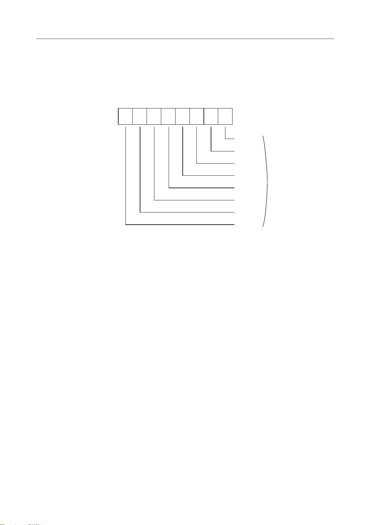
1. Inside message control register (X0hex)
This register performs various controls for a message.
Set this register for each message.
The bit configuration is as follows:
Address MSB
¥ 0h
76543210
LSB
ARES : Automatic transmission
FRM : Message format setting
EIT : Transmission completion interrupt enable
EIR : Receive completion interrupt enable
RCS : Receive status
TRQ : Transmission request
Not used
MMA : Message memory access enable
(1) Message memory access request/enable bit: MMA
This bit prevents contention between the microcontroller and CAN when accessing the
message memory.
When the microcontroller accesses the message memory, "1" is written to the MMA bit
regularly. The microcontroller confirms that the MMA bit is "1", and then accesses the
message memory. Write "0" to the MMA bit when the microcontroller accessing ends.
Operations by the MMA bit are shown in the following table.
At reset, the MMA bit is set to "0".
MMA
0
1
Microcontroller
Accesses from microcontroller
to message memory are disabled
Accesses from microcontroller
to message memory are enabled
Reception
Operate
Reading of received data
Stop
Rewriting of control area
Transmission
Operate
Stop
Rewriting of control area
Rewriting of transmission data
7/73
¡ Semiconductor
(2) Transmission request: TRQ
When a message is transmitted, the microcontroller writes "1" to this bit. When
transmission ends normally, CAN writes "0". This means that the TRQ bit is "1" during
transmission. Therefore, to request transmission, confirm that the TRQ bit is "0" first,
then write "1" to the TRQ bit. When the remote frame is received while the ARES bit is
"1", the TRQ bit is set to "1".
At reset, the TRQ bit is set to "0".
(3) Receive status: RCS
When receiving completes, the RCS bit becomes "1". Write "0" to the RCS bit before the
microcontroller calls up receive data. When receiving the remote frame, the RCS bit
becomes "1" just after the reception.
At reset, the RCS bit is set to "0".
(4) Receive completion interrupt enable: EIR
The microcontroller sets interrupt request signal generation disable/enable when
receiving completes.
The EIR bit is valid when the EINTR bit of the CANI register is “1”.
At reset, the EIR bit is set to "0".
MSM9225
(5) Transmission completion interrupt enable: EIT
The microcontroller sets interrupt request signal generation disable/enable when
transmission completes.
The EIT bit is valid when the EINTT bit of the CANI register is “1”.
At reset, the EIT bit is set to "0".
(6) Message format setting: FRM
The microcontroller sets the format of the message to be sent/received. A message in a
format other than the specified format cannot be sent/received.
For the relationship between setting and format, see the table below.
When a message specified to a group message is received, the content of the RTR bit is
written.
At reset, the FRM bit is set to "0".
FRM Message Type Transmission Format Receive Format
0
1
Standard message Data frame Remote frame
Group message Transmission disable Data frame
Standard message
Group message
Remote frame
Transmission disable
Data frame
Remote frame
(7) Automatic transmission : ARES
If the data frame is automatically transmitted after remote frame reception, the ARES bit
should be set to "1".
At reset, the ARES bit is set to "0".
8/73
¡ Semiconductor
g
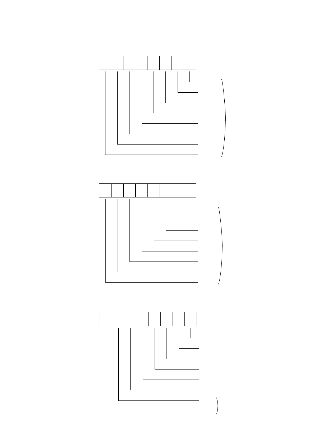
2. Identifier 0 (X1hex)
This register sets the data length code and a part of the identifier.
Set this register for each message.
The bit configuration is as follows:
MSM9225
Address MSB
¥ 1h
76543210
(1) Format setting: IDFM
The microcontroller sets the message format.
At reset, the IDFM bit is undefined.
IDFM Operation
0 Standard format (ID = 11 bits)
Extended format (ID = 29 bits)I
LSB
IDB26 :
IDB27 :
IDB28 :
DLC0 :
DLC1 :
DLC2 :
DLC3 :
IDFM : Format settin
Identifier
Data length code
(2) Data length code: DLC3 to DLC0
This is control field data to set the number of bytes of a data field. 0 to 8 can be set.
At reset, these bits are undefined.
(3) Identifier: IDB28 to IDB26
These bits set the identifier field.
For standard format (IDFM = 0), the higher 3 bits of the 11 bits are set.
For extended format (IDFM = 1), the higher 3 bits (ID28 to ID26) of the 29 bits (ID28 to
ID0) are set.
At reset, these bits are undefined.
9/73
¡ Semiconductor
3. Identifier 1 (X2hex)
This register sets the identifier.
Set this register for each message.
The bit configuration is as follows:
MSM9225
Address MSB
¥ 2h
76543210
LSB
IDB18 :
IDB19 :
IDB20 :
IDB21 :
Identifier
IDB22 :
IDB23 :
IDB24 :
IDB25 :
(1) Identifier: IDB25 to IDB18
These bits set the lower 8 bits of the 11 bits of the identifier field.
For standard format (IDFM = 0), the lower 8 bits of the 11 bits are set.
For extended format (IDFM = 1), ID25 to ID18 of the 29 bits (ID28 to ID0) are set.
At reset, these bits are undefined.
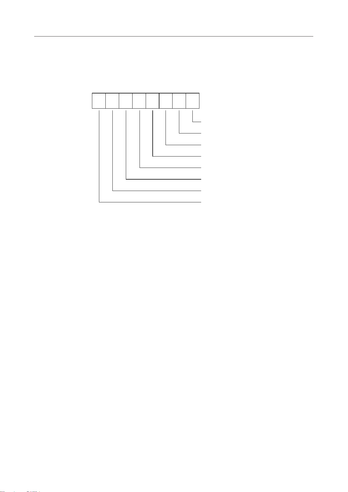
4. Address: X3 to XDhex
For standard format (IDFM = 0), addresses X3 to XAhex become the transmission/receive
data storage area.
For extended format (IDFM = 1), addresses X3 to X5hex are used to set the identifier field, and
addresses X6 to XDhex become the transmission/receive data storage area.
For both, a maximum of 8 bytes of transmission/receive data can be stored, but the number
of transmittable/receivable bytes must have been set by data length code.
At reset, message content is undefined.
The relationship between address and identifier bits for extended format (IDFM = 1) is as
follows:
10/73
¡ Semiconductor
MSM9225
Adderss MSB
¥ 3h
Address MSB
¥ 4h
LSB
76543210
IDB10 :
IDB11 :
IDB12 :
IDB13 :
Identifier 2
IDB14 :
IDB15 :
IDB16 :
IDB17 :
LSB
76543210
Address MSB
¥ 5h
IDB2 :
IDB3 :
IDB4 :
IDB5 :
Identifier 3
IDB6 :
IDB7 :
IDB8 :
IDB9 :
LSB
76543210
Not used (Don't care)
Not used (Don't care)
Not used (Don't care)
Not used (Don't care)
Not used (Don't care)
Not used (Don't care)
IDB0 :
Identifier 4
IDB1 :
11/73

¡ Semiconductor
Control Register
These registers listed below control various operations of CAN.
MSM9225
Address Symbol
0EH CANC
0FH CANI
1EH NMES Number of message specification registers
1FH BTR0 CAN bus timing register 0
2EH BTR1 CAN bus timing register 1
2FH TIOC Communication input/output control register
3EH GMR0 Group message register 0
3FH GMR1 Group message register 1
4EH GMSK00 Message mask register 00
4FH GMSK01 Message mask register 01
5EH GMSK02 Message mask register 02
5FH GMSK03 Message mask register 03
6EH GMSK10 Message mask register 10
6FH GMSK11 Message mask register 11
7EH GMSK12 Message mask register 12
7FH GMSK13 Message mask register 13
8EH STBY Standby control register
8FH Not used (reserve area)
9EH TMN Communication message number register
9FH CANS CAN status register
AEH TEC Transmission error counter
AFH REC Receive error counter
BEH
BFH
CEH
CFH
DEH
DFH
EEH
EFH
FEH
FFH
CAN control register
CAN interrupt control register
Not used (reserve area)
Name
12/73
¡ Semiconductor
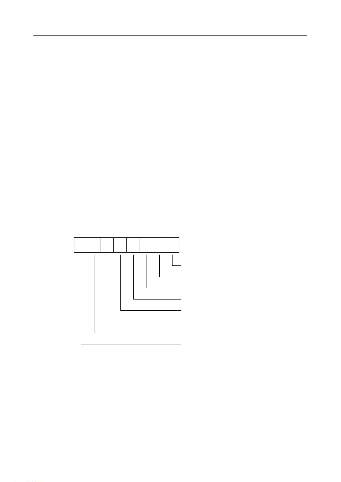
1. CAN control register (CANC: 0Ehex)
This register controls the operation of CAN.
The bit configuration is as follows:
MSM9225
Address MSB
0Eh
76543210
LSB
INIT : Initialize
TIRS : Transmission identifier retrieval
Not used
SYNC : Bit synchronization
CANA : CAN write flag
T x F : Transmission flag
R x F : Receive flag
Not used
(1) Initialize: INIT
This bit is used to initialize the communication control area. To start initialization, write
"1" to INIT, read INIT and confirm that INIT is "1", then initialize. To end initialization,
write "0" to INIT, read INIT, and confirm that INIT is "0". For both, initialization mode
is not set/cleared until the above procedure is executed.
If the INIT bit is set to "1" during the transmission or receive operation, the initialization
will start after the communication completes.
When the INIT bit is set to "1", the communication operation stops but the error counter
and data memory are held.
To initialize message memory, write the number of messages to be used to the number
of messages setting register, NMES, then write the inside message control register,
identifier 1, and identifier 2 sequentially from message 0 for all messages.
At reset, INIT is set to "1".
(2) Transmission identifier retrieval: TIRS
This bit is used to scan identifiers sequentially from message 0 to the last message of the
message memory, detecting priority of the message for which the transmission request
TRQ is "1" and starting to transmit the messages. TIRS will be set to "0" when there are
no transmission request messages after scanning or transmitting.
At reset, TIRS is set to "0".
(3) Bit synchronization: SYNC
This bit is used to set the bit synchronization edge to synchronize at the CAN bus.
When SYNC is "0", the synchronization edge is set at the falling edge of data.
When SYNC is "1", the synchronization edge is set at both the rising and falling edges of
data.
At reset, SYNC is set to "0".
13/73
¡ Semiconductor
p
(4) CAN write flag: CANA
This bit is used to indicate receive data write status to the message memory. CANA is
"1" while CAN is writing receive data to the message memory.
This is a read-only flag.
(5) Transmission flag: TxF
This bit is used to indicate transmission operation status.
When TxF is "0", CAN is in transmission operation stop status.
When TxF is "1", CAN is in transmission operation status. TxF becomes "0" when
transmission completes.
This is a read-only flag.
(6) Receive flag: RxF
This bit is used to indicate receive operation status.
When RxF is "0", CAN is in receive operation stop status.
When RxF is "1", CAN is in receive operation status. RxF becomes "0" when receiving
completes.
This is a read-only flag.
MSM9225
2. CAN interrupt register (CANI: 0Fhex)
This register controls CAN interrupts.
The bit configuration is as follows:
Address MSB
0Fh
76543210
(1) Transmission interrupt output enable: EINTT
This bit is used to output transmission interrupt signal INTT from interrupt pin INT
when transmission completes.
When EINTT is "0", a transmission interrupt signal is not output from the interrupt pin.
When EINTT is "1", a transmission interrupt signal is output from the interrupt pin.
At reset, EINTT is set to "0".
LSB
EINTT : Transmission interrupt output enable
EINTR : Receive interrupt output enable
EINTE : Error interrupt output enable
Not used
ITF : Transmission interrupt request flag
IRF : Receive interrupt request flag
IEF : Error interrupt request flag
MEINT : Master interru
t control enable
(2) Receive interrupt output enable: EINTR
This bit is used to output receive interrupt signal INTR from interrupt pin INT when
reception completes.
When EINTR is "0", a receive interrupt signal is not output from the interrupt pin.
When EINTR is "1", a receive interrupt signal is output from the interrupt pin.
At reset, EINTR is set to "0".
14/73
¡ Semiconductor
(3) Error interrupt output enable: EINTE
When an error occurs, this bit is used to output error interrupt signal INTE from interrupt
pin INT.
When EINTE is "0", an error interrupt signal is not output from the interrupt pin.
When EINTE is "1", an error interrupt signal is output from the interrupt pin.
At reset, EINTE is set to "0".
(4) Transmission interrupt request flag: ITF
ITF becomes "1" when a transmission interrupt is generated. Only "0" can be written to
this bit.
At reset, ITF is set to "0".
(5) Receive interrupt request flag: IRF
IRF becomes "1" when a receive interrupt is generated. Only "0" can be written to this bit.
At reset, IRF is set to "0".
(6) Error interrupt request flag: IEF
IEF becomes "1" when an error occurs. Only "0" can be written to this bit.
At reset, IEF is set to "0".
MSM9225
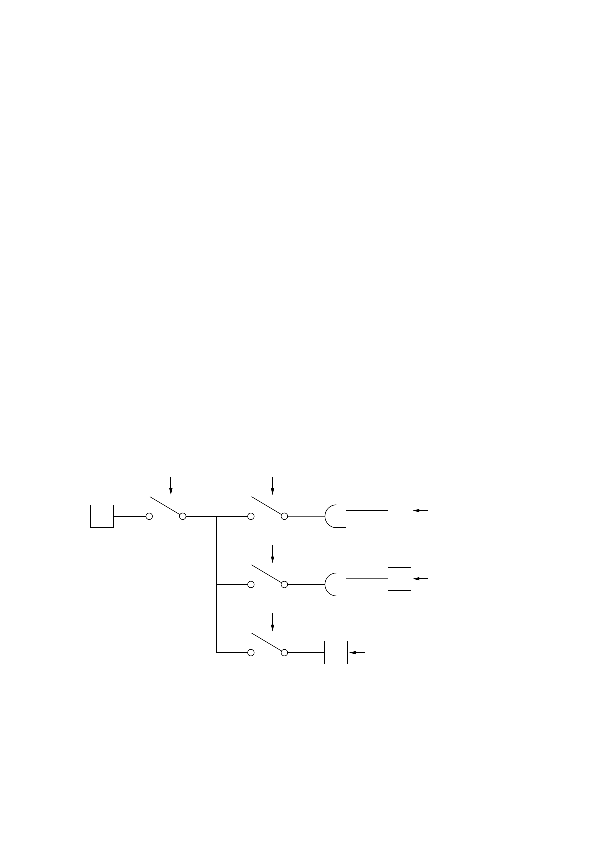
(7) Master interrupt control enable: MEINT
This bit is used to set enable/disable of communication interrupts.
The flowchart of interrupt control is shown below.
When MEINT is "0", interrupt request control is disabled.
When MEINT is "1", interrupt request control is enabled.
At reset, MEINT is set to "0".
MEINT
0
1
0
1
0
1
INT pin
0
1
EINTT
EINTR
EINTE
ITF
Interrupt factor
(transmission completion)
EIT (each message)
IRF
Interrupt factor
(reception completion)
EIR (each message)
IEF
Interrupt factor (An error occurs)
15/73
¡ Semiconductor
3. Number of messages specification register (NMES: 1Ehex)
This is a register to set the number of messages to be stored in the message memory.
A maximum of 16 messages can be set, with message numbers 0 to 15.
Writing to NMES is enabled when initialize bit INIT of the CAN control register (CANC:
OEhex) is "1".
At reset, NMES is set to "0000".
The bit configuration and relationship between message number and number of messages
are as follows:
MSM9225
Address MSB
1Eh
***
*
****
****
········
···· · · · ·
****
****
: Don't Care
*
4. CAN bus timing register 0 (BTR0: 1Fhex)
This register sets the baud rate prescaler and synchronization jump width (SJW) used for bus
timing. Writing to the BTR0 bit is enabled, when the INIT bit of the CAN control register
(CANC: 0Ehex) is "1".
The bit configuration is as follows:
Address MSB
1Fh
76543210
NMES3 NMES2 NMES1 NMES0
0000
0000
1110
1111
LSB
LSB
Number of message
1
2
·
·
15
16
BRP0 :
BRP1 :
BRP2 :
BRP3 :
BRP4 :
BRP5 :
SJWA :
SJWB :
Baud rate
prescaler
Synchronization
Jump Width
16/73
¡ Semiconductor
(1) Baud rate prescaler: BRP5 to BRP0
This is a 6-bit prescaler to set the BTL cycle time and SJW of the basic clock for
communication operation.
The relationship between the bit content and BTL is as follows:
At reset, BRP5 to BRP0 are set to "000000".
BRP5 BRP3 BRP2 BRP1 BRP0
BRP4
00000
00001
·····
·····
11110
1
0
0
·
·
1
11111
The BTL cycle time is given by the following operation.
BTL cycle time = 2 ¥ (25 ¥ BRP5 + 24 ¥ BRP4 + 23 ¥ BRP3 + 22 ¥ BRP2 + 21 ¥ BRP1 + BRP0
+ 1)/f
OSC
*) System clock is 1/2 division of oscillation frequency.
f
is the oscillation frequency.
OSC
MSM9225
BTL cycle time
1X system clock cycle
2X system clock cycle
·
·
63X system clock cycle
64X system clock cycle
(2) SJW: SJWA, SJWB
This is a 2-bit register to set SJW.
The relationship between bit content and SJW is as follows:
At reset, SJWA and SJWB are set to “00”.
SJWB SJWA SJW1, SJW2
001 ¥ BTL cycle
012 ¥ BTL cycle
103 ¥ BTL cycle
114 ¥ BTL cycle
17/73
¡ Semiconductor
MSM9225
5. CAN bus timing register 1 (BTR1: 2Ehex)
This register sets the sampling count, sampling point and transmit point used for bus timing.
Writing to the BTR1 bit is enabled, when the INIT bit of the CAN control register (CANC:
0Ehex) is "1".
The bit configuration is as follows:
Address MSB
2Eh
76543210
LSB
(1) Time segment 1: TSEG13 to TSEG10
This is a 4-bit register to set the sampling point.
The relationship between bit content and TSEG1 is as follows:
At reset, TSEG13 to TSEG10 are set to "0000".
TSEG10 :
TSEG11 :
TSEG12 :
TSEG13 :
TSEG20 :
TSEG21 :
TSEG22 :
Not used :
Time
segment 1
Time
segment 2
TSEG13 TSEG12 TSEG11 TSEG10 TSEG1
0000
0001
····
····
1110
1111
1 ¥ BTL cycle
2 ¥ BTL cycle
·
·
15 ¥ BTL cycle
16 ¥ BTL cycle
(2) Time segment 2: TSEG22 to TSEG20
This is a 3-bit register to set the transmit point.
The relationship between the bit content and TSEG2 is as follows:
At reset, TSEG22 to TSEG20 are set to "000".
TSEG22 TSEG21 TSEG20 TSEG2
000
001
···
···
110
111
1 ¥ BTL cycle
2 ¥ BTL cycle
·
·
7 ¥ BTL cycle
8 ¥ BTL cycle
18/73
¡ Semiconductor
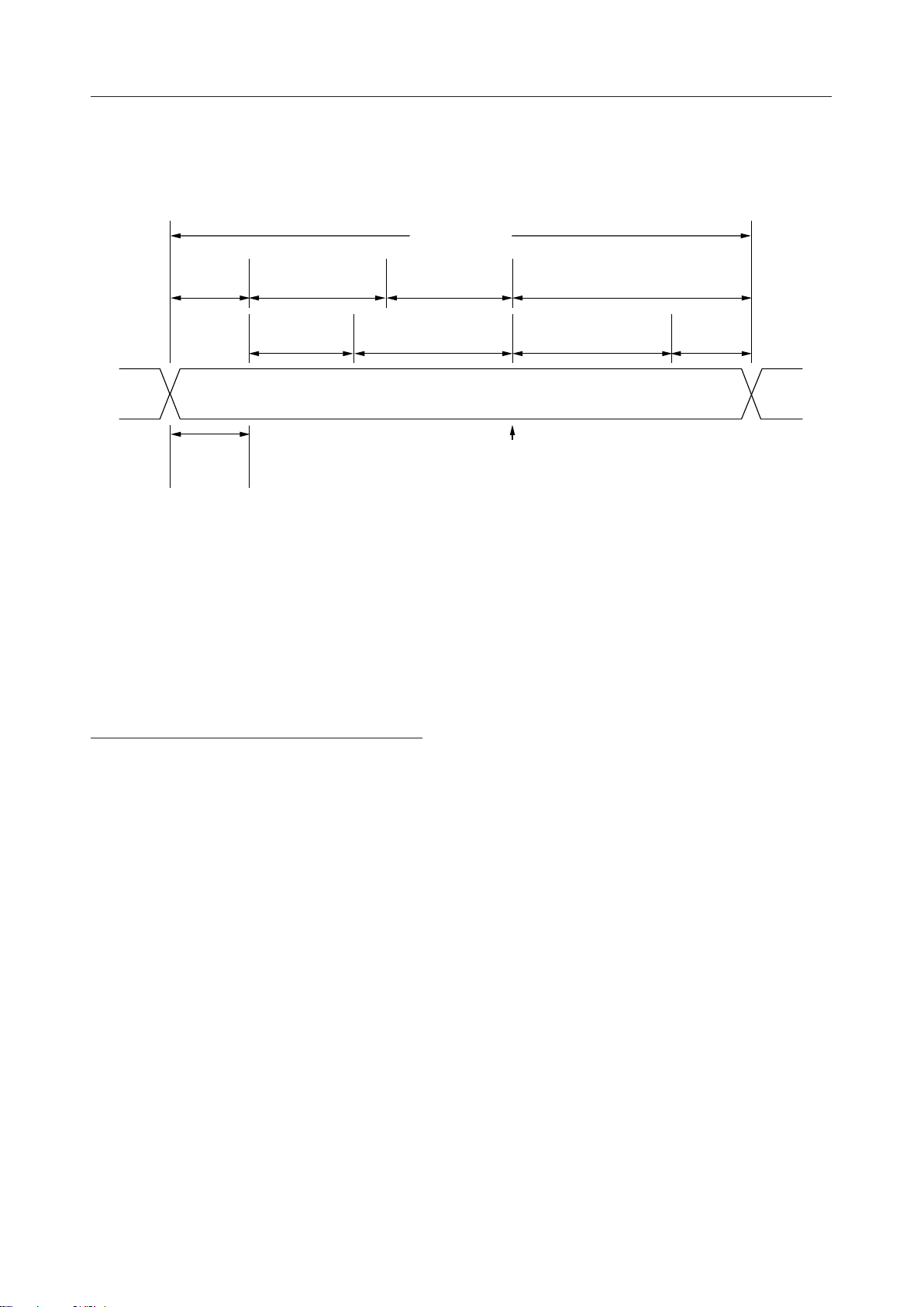
(3) Bit timing
Bit timing is set by CAN bus timing registers 0 and 1. The relationship between 1 bit time
of a message and a CAN bus timing (the MSM9225 register) is as follows:
MSM9225
1 bit time
PROP-SEGSYNC-SEG PHASE-SEG1 PHASE-SEG2
SJW1
(BTR0 : SJWB/A)
1BTL
cycle
If setting is :
BTR0 = "01000001" ...SJWB = "0" SJWA = "1" BRP5-0 = "000001"
BTR1 = "00000001"...TSEG2 = "000" TSEG1 = "0001"
then the bit timing is as follows
Sync segment 1 BTL cycle (fixed)
SJW 1 2 BTL cycle
TSEG 1 2 BTL cycle
TSEG 2 1 BTL cycle
SJW 2 2 BTL cycle
1 bit time 8 BTL cycle
TSEG1
(BTR1 : TSEG13-10)
Sampling
TSEG2
(BTR1 : TSEG22-20)
point
SJW2
(= SJW1)
Sampling point = 5 BTL cycle
If f
= 16 MHz, then 1 BTL cycle is :
osc
BTL cycle = 2 ¥ (25 ¥ 0 + 24 ¥ 0 + 23 ¥ 0 + 22 ¥ 0 + 21 ¥ 0 + 1 + 1) / 16 MHz = 0.25 ms
Therefore 1 bit time is :
8 BTL cycle = 8 ¥ 0.25 ms = 2.0 ms
(= 500 Kb/s)
6. Communication input/output control register (TIOC: 2Fhex)
This register sets the communication mode and output buffer format.
Writing to the TIOC bit is enabled, when the INIT bit of the CAN control register (CANC:
0Ehex) is "1".
The bit configuration is as follows:
19/73
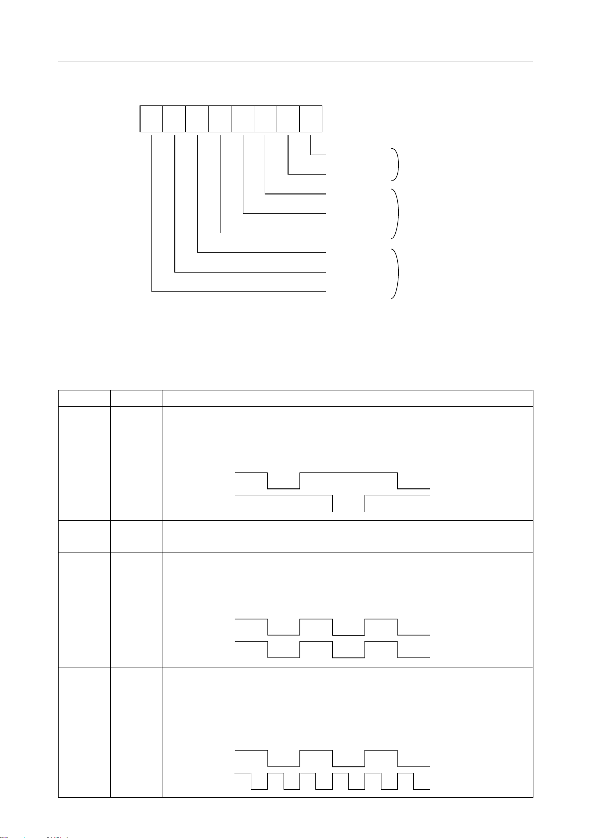
¡ Semiconductor
MSM9225
Address MSB
2Fh
76543210
LSB
OCMD0
OCMD1
OCPOL0
OCTN0
OCTP0
OCPOL1
OCTN1
OCTP1
:
Output mode
:
:
:
buffer format
:
:
:
buffer format
:
Tx0 output
Tx1 output
(1) Time segment 1: OCMD1 to OCMD0
These bits are used to set the output mode of output pins Tx0 and Tx1.
The relationship between the bit content and output mode is as follows:
At reset, OCMD1 to OCMD0 are set to “00”.
setting
OCMD1 OCMD0
00
01
10
11
Output mode of Tx0 and Tx1
[Double layer mode]
Transmission data "0" is output from Tx0 and Tx1 altermately.
Output example
Data
Tx0
Tx1
[Disabled]
[Single layer mode]
Same bit string data is output from both Tx0 qnd Tx1.
Output example
Data
Tx0
Tx1
[Clock output mode]
Bit string data is output from Tx0.
Synchrinization clock is output from Tx1.
Output example
Data
101010
101010
101010
Tx0
Tx1
20/73
¡ Semiconductor
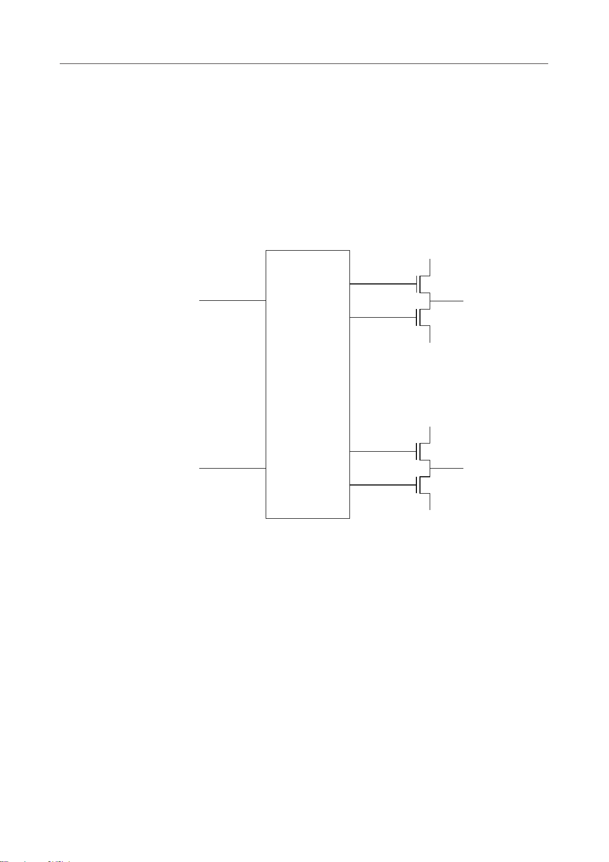
(2) Output driver format setting: OCPOL, OCTN, OCTP
OCPOL is used to set the polarity of output.
OCTN is used to set the open/drain mode of the Nch transistor of the output driver.
OCTP is used to set the open/drain mode of the Pch transistor of the output driver.
The circuit configuration of the output driver and the relationship between bit content
and output driver format are as follows:
At reset, all bits are set to "0".
MSM9225
Output data
Synchronization
clock
Circuit configuration
Output control
circuit
V
DD
P
ch
N
ch
GND
V
DD
P
ch
N
ch
GND
Tx0
Tx1
21/73

¡ Semiconductor
Mode OCTP OCTN OCPOL Output data Pch Tr Nch Tr Tx pin output level
Floating
Pulldown
Pullup
Push-pull
Output driver format
0 0 0 0 off off
0 0 0 1 off off
0 0 1 0 off off
0 0 1 1 off off
0 1 0 0 off on
0 1 0 1 off off
0 1 1 0 off off
0 1 1 1 off on
1 0 0 0 off off
100 1 onoff
101 0 onoff
1 0 1 1 off off
1 1 0 0 off on
110 1 onoff
111 0 onoff
1 1 1 1 off on
MSM9225
Floating
Floating
Floating
Floating
"0"
Floating
Floating
"0"
Floating
"1"
"1"
Floating
"0"
"1"
"1"
"0"
22/73
¡ Semiconductor
MSM9225
7. Group message register (GMR0: 3Ehex, GMR1: 3Fhex)
These are registers to set the group message mode.
Two messages can be set to the group message mode.
At reset, all bits are set to "0".
The group message mode is valid when the EGM0/EGM1 bit is "1".
Using GMR03 to GMR00 and GMR13 to GMR10, set the message numbers of messages that
are to be set to the group message mode.
The bit configuration is as follows:
Address MSB
3Eh
3Fh
EGM0
EGM1 0 0 0 GMR11 GMR12 GMR11 GMR10
0 0 0 GMR03 GMR02 GMR01 GMR00
LSB
8. Group message mask register (GMSK)
This is a register to judge identifiers when a message with a message number specified by the
group message mode GMR is received.
Using MiID28 to MiID0, set the bits to mask the identifier of a message set by the GMR bit.
Setting "1" masks the bit, setting "0" does not mask the bit.
(M0ID28 to M0ID0 are for GMR0, and M1ID28 to M1ID0 are for GMR1.)
At reset, all bits are set to "0".
The bit configuration is as follows:
Address MSB
4Eh
4Fh
M0ID28
M0ID20 M0ID19 M0ID18 M0ID17 M0ID16 M0ID15 M0ID14 M0ID13
M0ID27 M0ID26 M0ID25 M0ID24 M0ID23 M0ID22 M0ID21
LSB
GMR0
GMR1
GMSK00
GMSK01
5Eh
5Fh
Address MSB
6Eh
6Fh
7Eh
7Fh
M0ID12
M0ID4 M0ID3 M0ID2 M0ID1 M0ID0 0 0 0
M1ID28
M1ID20 M1ID19 M1ID18 M1ID17 M1ID16 M1ID15 M1ID14 M1ID13
M1ID12
M1ID4 M1ID3 M1ID2 M1ID1 M1ID0 0 0 0
M0ID11 M0ID10 M0ID9 M0ID8 M0ID7 M0ID6 M0ID5
LSB
M1ID27 M1ID26 M1ID25 M1ID24 M1ID23 M1ID22 M1ID21
M1ID11 M1ID10 M1ID9 M1ID8 M1ID7 M1ID6 M1ID5
GMSK02
GMSK03
GMSK10
GMSK11
GMSK12
GMSK13
23/73
 Loading...