

OKI MSM9210GS-BK, MSM9210GS-2K Datasheet

E2C0038-39-95
¡ Semiconductor
¡ Semiconductor
This version: Sep. 1999
Previous version: Aug. 1999
MSM9210
MSM9210
32-Bit Duplex/Triplex (1/2 duty / 1/3 duty) VF Controller/Driver with Digital Dimming
GENERAL DESCRIPTION
The MSM9210 is a full CMOS controller/driver for Duplex or Triplex (1/2 duty or 1/3 duty)
vacuum fluorescent display tube. It consists of a 32-segment driver multiplexed to drive up to
96 segments, and 10-bit digital dimming circuit.
MSM9210 features a selection of a master mode and a slave mode, and therefore it can be used
to expand segments for the VFD driver with keyscan and A/D converter function.
MSM9210 provides an interface with a microcontroller only by three signal lines: DATA IN,
CLOCK and CS.
FEATURES
• Logic supply voltage (VDD) : 4.5 to 5.5V
• Driver supply voltage (V
• Duplex/Triplex (1/2 duty / 1/3 duty) selectable
DUP/TRI=1/2 duty selectable at "H" level
DUP/TRI=1/3 duty selectable at "L" level
• Number of display segments
Max. 64-segment display (during 1/2 duty mode)
Max. 96-segment display (during 1/3 duty mode)
• Master/Slave selectable
M/S=Master mode selectable at "H" level
M/S=Slave mode selectable at "L" level
• Interface with a microcontroller
Three lines: CS, CLOCK, and DATA IN
• 32-segment driver outputs : IOH=–5mA at VOH=V
(can be directly connected to VFD tube : IOH=–10mA at VOH=V
and require no external resisters) : IOL=500mA at VOL=2V (SEG1 to 32)
• 3-grid pre-driver outputs : IOH=–5.0mA at VOH=V
(require external drivers) IOL=10mA at VOL=2V
• Logic outputs : IOH=–200mA at VOH=VDD–0.8V
• Built-in digital dimming circuit (10-bit resolution)
• Built-in oscillation circuit (external R and C)
• Built-in Power-On-Reset circuit
• Package options:
56-pin plastic QFP (QFP56-P-910-0.65-2K) Product name: MSM9210GS-2K
64-pin plastic QFP (QFP64-P-1414-0.80-BK) Product name: MSM9210GS-BK
) : 8 to 18V
DISP
IOL=200mA at VOL=0.8V
–0.8V (SEG1 to 22)
DISP
–0.8V (SEG23 to 32)
DISP
–0.8V
DISP
1/19
¡ Semiconductor
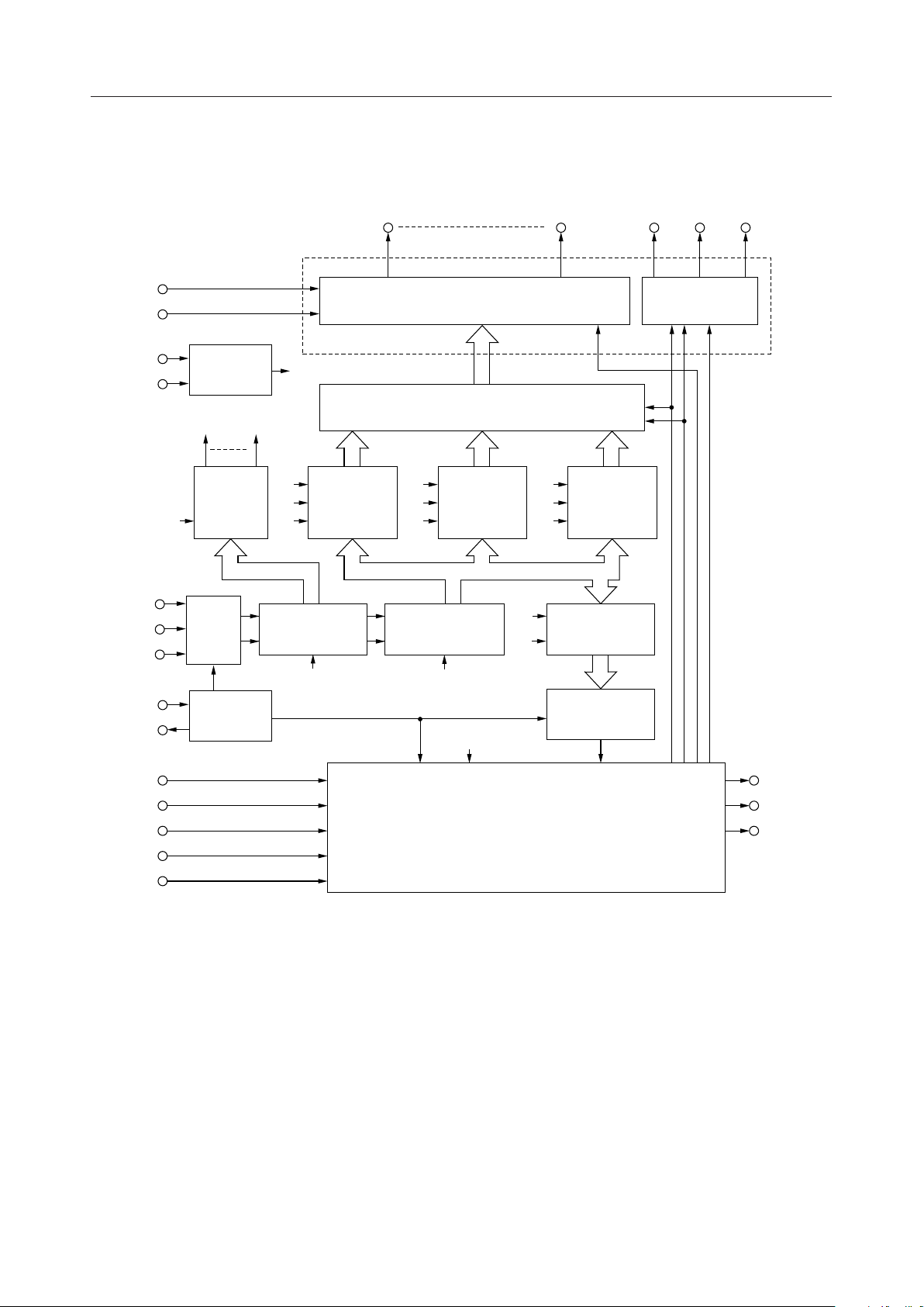
BLOCK DIAGRAM
V
DISP
D-GND
32 Segment Driver
MSM9210
GRID2 GRID3GRID1SEG32SEG1
3 Grid pre Driver
V
DD
L-GND
CS
CLOCK
DATA IN
OSC0
OSC1
DIM IN
SYNC IN1
SYNC IN2
M/S
DUP/TRI
POR
Power
On
Reset
0H 4H
Mode Select
in1-3
Control
OSC
POR
1H
0H
POR
Out1-32
Segment Latch
1
in1-32
Out1-3
3bit Shift Register
POR
Out1-32
96 to 32 Segment Control
in1-32in1-32 in1-32in1-32
2H
0H
POR
Out1-32
Segment Latch
2
in1-32
Out1-32
32bit Shift Register
POR
POR
Timing Generator
4H
POR
3H
Segment Latch
0H
POR
Dimming Latch
Out1-10
10bit Digital
Dimming
Out1-32
3
in1-32
in1-10
DIM OUT
SYNC OUT1
SYNC OUT2
2/19
¡ Semiconductor
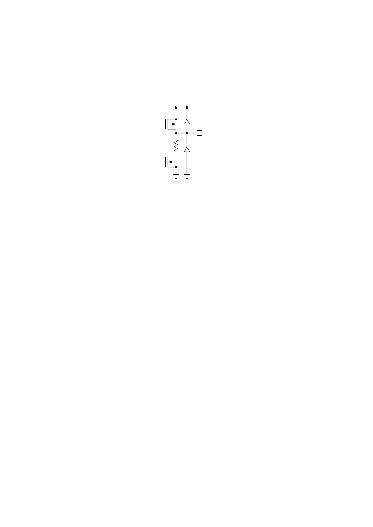
INPUT AND OUTPUT CONFIGURATION
Schematic Diagram of Driver Output Circuit
MSM9210
V
D-GND
DISP
V
DISP
OUTPUT
D-GND
3/19
¡ Semiconductor
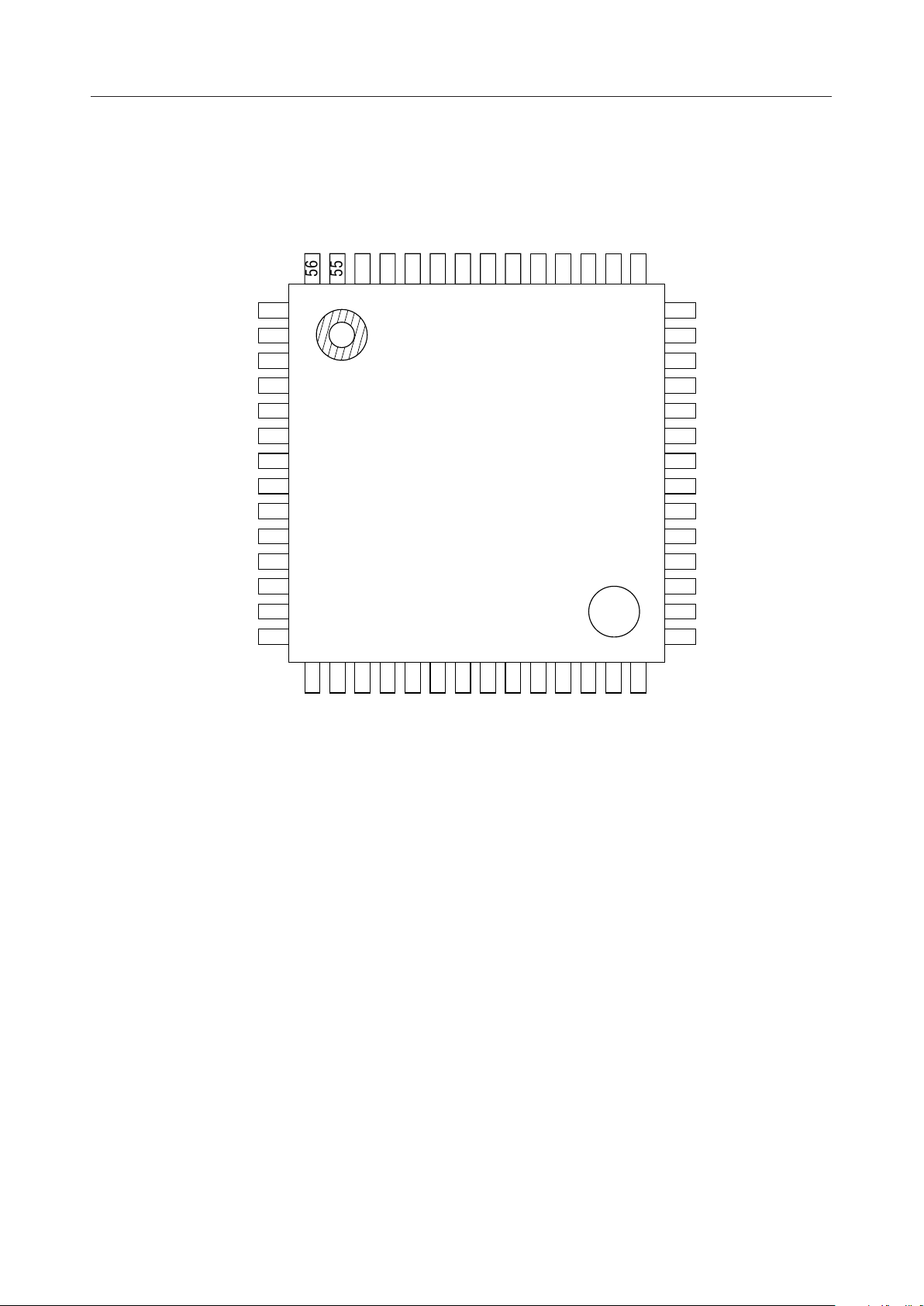
PIN CONFIGURATION (TOP VIEW)
MSM9210
SEG25
SEG26
SEG27
SEG28
SEG29
SEG30
SEG31
SEG32
GRID1
GRID2
GRID3
DD
10
11
12D-GND
13NC
14V
DISP
SEG24
SEG23
SEG22
SEG21
SEG20
SEG19
D-GND
49
22
SEG18
48
47 SEG17
23
24DUP/TRI
46 SEG16
45 SEG15
25M/S
26SYNC OUT 2
V
56
55
54
53
52
51
50
1
2
3
4
5
6
7
8
9
15
16
17
18
19
20
21
DISP
44 SEG14
43 V
42
41
40
39
38
37
36
35
34
33
32
31 SEG2
30 SEG1
29 NC
27SYNC OUT 1
28DIM OUT
SEG13
SEG12
SEG11
SEG10
SEG9
SEG8
SEG7
SEG6
SEG5
SEG4
SEG3
DIM IN
SYNC IN 1
CS
OSC1
CLOCK
SYNC IN 2
L-GND
DATA IN
NC: No connection
56-pin Plastic QFP
OSC0
4/19
¡ Semiconductor
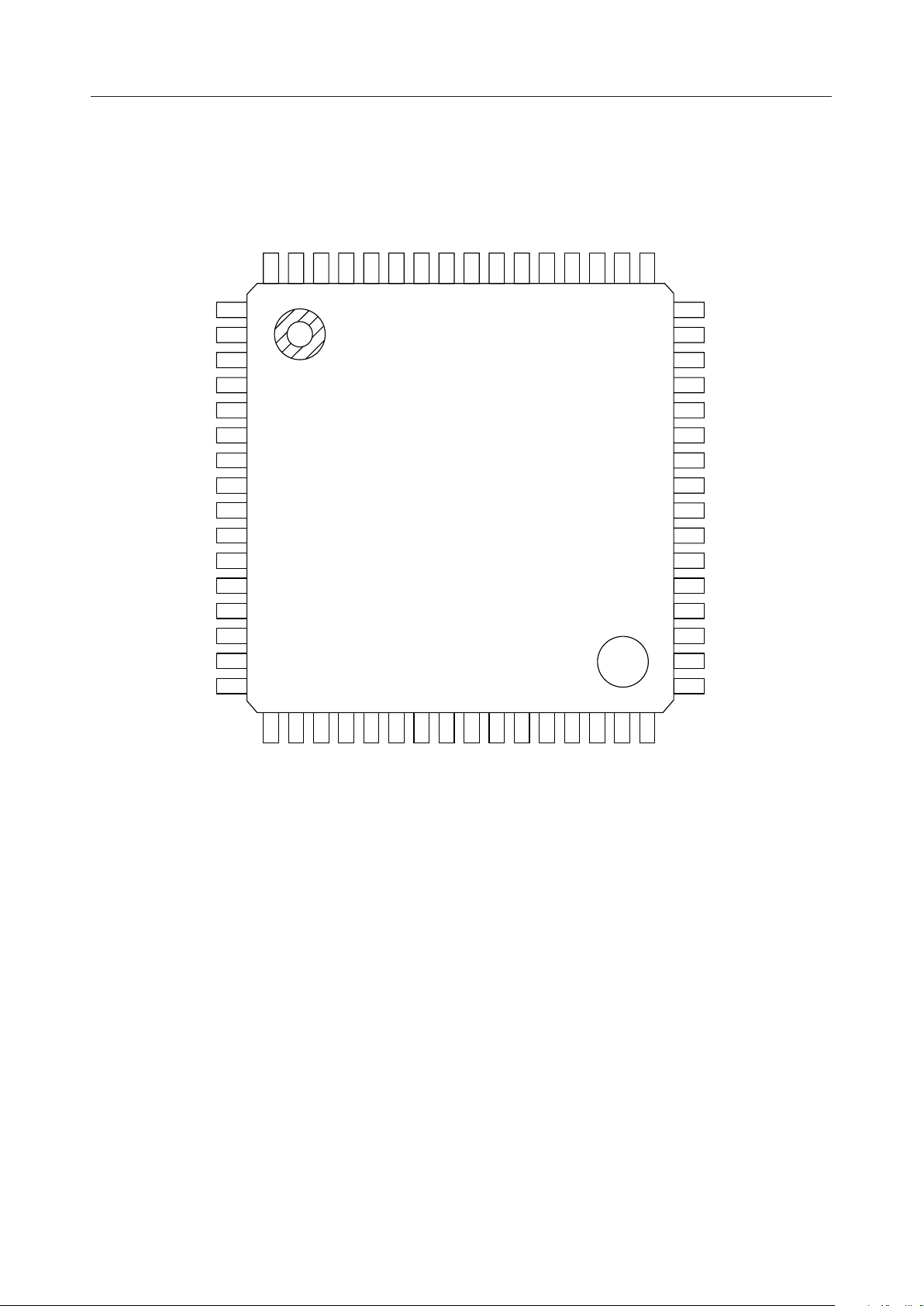
MSM9210
NC
SEG25
SEG26
SEG27
SEG28
SEG29
SEG30
SEG31
SEG32
GRID1
GRID2
GRID3
D-GND
NC
V
DD
NC
10
11
12
13
14
15
16
DISP
NC
SEG24
SEG23
SEG22
SEG21
SEG20
SEG19
D-GND
SEG18
55
SEG17
SEG1652SEG1551SEG1450NC49V
54
53
V
64
63
62
61
60
59
58
57
56
1
2
3
4
5
6
7
8
9
DISP
48
47
46
45
44
43
42
41
40
39
38
37
36
35
34
33
NC
NC
SEG13
SEG12
SEG11
SEG10
SEG9
SEG8
SEG7
SEG6
SEG5
SEG4
SEG3
SEG2
SEG1
NC
17
NC
18
19
DIM IN
SYNC IN1
20
21
22
23
24
CS
CLOCK
SYNC IN2
L-GND
DATA IN
NC: No connection
64-pin Plastic QFP
25
OSC1
26
OSC0
27
DUP/TRI
28
29
M/S
SYNC OUT2
30
31
32
NC
DIM OUT
SYNC OUT1
5/19
¡ Semiconductor
PIN DESCRIPTIONS
MSM9210
Symbol
QFP56
V
DISP
V
DD
43,56 —
14 —
D-GND 12, 49 —
L-GND 21 —
30 to 42,
SEG1 to 22
44 to 48,
50 to 53
1 to 8,
SEG23 to 32
54, 55
GRID1 to 3 9, 10, 11 O
CS 18 I
CLOCK 19 I
DATA IN 20 I
DUP/TRI 24 I
QFP64
49,64
15
13, 56
24
34 to 46,
51 to 55,
57 to 60
2 to 9,
61, 62
10, 11, 12
21
22
23
27
Type Description
Pin
Power supply pins for VFD driver circuit.
43 pin and 56 pin should be connected externally.
Power supply pin for logic drive.
D-GND is ground pin for the VFD driver circuit. L-GND is ground
pin for the logic circuit. 12pin, 21pin and 49pin should be
connected externally.
Segment (anode) signal output pins for a VFD tube.
These pins can be directly connected to the VFD tube.
O
External circuit is not required.
IOH£–5 mA
Segment (anode) signal output pins for a VFD tube.
These pins can be directly connected to the VFD tube.
O
External circuit is not required.
IOH£–10 mA
Inverted Grid signal output pins.
For pre-driver, the external circuit is required.
IOL£10 mA
Chip select input pin.
Data is not transferred when CS is set to a Low level.
Shift clock input pin.
Serial data shifts at the rising edge of the CLOCK.
Serial data input pin (positive logic).
Data is input to the shift register at the rising edge of the CLOCK signal.
Duplex/Triplex operation select input pin.
Duplex (1/2 duty) operation is selected when this pin is set to V
Triplex (1/3 duty) operation is selected when this pin is set to L-GND.
DD
.
M/S 25 I
DIM IN 15 I
28
18
Master/Slave mode select input pin.
Master mode is selected when this pin is set to V
DD
.
Slave mode is selected when this pin is set to L-GND.
Dimming pulse input.
When the slave mode is selected, the pulse width of the all segment
output are controlled by a input pulse width of DIM IN.
Connect this pin to the master side DIM OUT pin at the slave mode.
When the master mode is selected, the input level of this pin is
ignored and the pulse width of the all grids and segment outputs are
controlled by a built-in 10-bit dimming circuit.
Connect this pin to V
or L-GND at the master mode.
DD
6/19
 Loading...