

OKI MSM9000-xxAV-Z-xx, MSM9000-xx Datasheet

E2B0041-27-Y3
¡ Semiconductor
¡ Semiconductor
This version: Nov. 1997
Previous version: Mar. 1996
MSM9000B-xx
MSM9000B-xx
DOT MATRIX LCD CONTROLLER
GENERAL DESCRIPTION
The MSM9000B-xx is a dot-matrix LCD control driver which has functions of displaying 12 (5
x 7 dots) characters (2 lines) and 120-dot arbitrators.
The MSM9000B-xx is provided with a 16-dot common driver, 60-dot segment driver, Display
Data RAM (DDRAM), and Character Generator ROM (CGROM).
This device can be controlled with commands entered through the serial interface or parallel
interface.
The font data in the CGROM can be changed by mask option.
Since the MSM9000B-xx has an LCD driving bias generator circuit, LCD bias voltages can be
obtained by merely providing a required capacitance externally.
The MSM9000B-xx is applicable to a variety of LCD panels by controlling the contrast.
FEATURES
• Logic voltage(VDD): 2.5 to 3.3 V
• LCD driving voltage(VBI) : 3.0 to 5.5 V
• Low current consumption: 35 mA max.(operating)
• Switchable between 8-bit serial interface and 8-bit parallel interface
• Contains a 16-dot common driver and a 60-dot segment driver
• Contains CGROM with character fonts of (5 x 7 dots) x 256
• Built-in bias voltage generator circuit
• Built-in contrast adjusting circuit
• Built-in 32.768 kHz crystal oscillator circuit
• Provided with 120 dot arbitrators
• 1/9 duty mode (1 line : characters, 2 lines : arbitrators)
1/16 duty mode (2 lines : characters, 2 lines : arbitrators)
• Character blink operation can be switched between all-character lighting-on mode and allcharacter lighting-off mode.
• Package:
TCP mounting with 35 mm wide film ; Tin-plated (Product name : MSM9000B-xx AV-Z-xx)
Chip (Product name : MSM9000B-xx)
xx indicates code number.
1/38
¡ Semiconductor
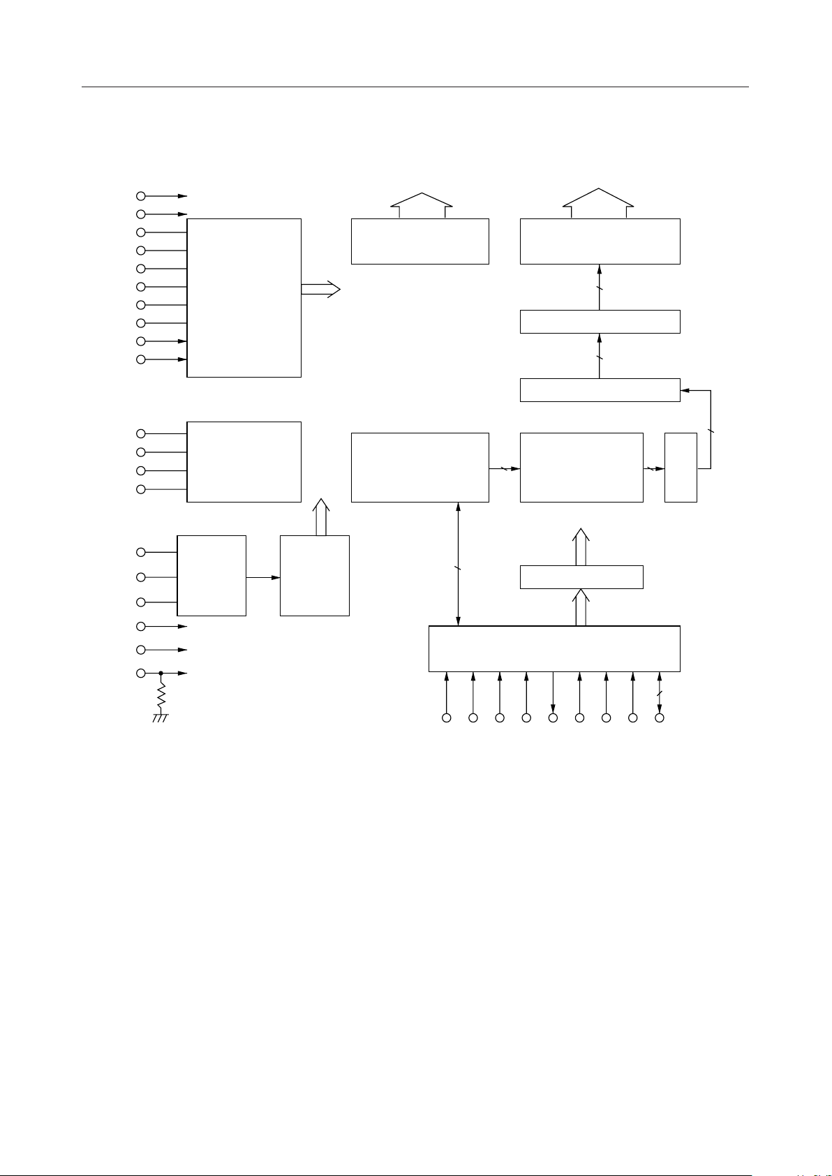
BLOCK DIAGRAM
MSM9000B-xx
V
DD
V
SS
V
SS1
V
SS2, 3
V
SS4
V
SS5
V
C2
V
CC2
N1
N2
V
SS6
V
SH
V
C1
V
CC1
XT
XT
32K/EXT
Regulator
+
Halver & Voltage
Multiplier(4-fold)
Voltage Multiplier
(3/2-fold)
Crystal OSC
Circuit
Timing
Circuit
C1-C16
Common
Driver
LCD bias
Display Data RAM
(DDRAM) (456 Bits)
S1-S60
6016
Segment Driver
60
Latch
60
Shift Register
5
Character Generator
8
ROM (CGROM)
F/F
5
Gate
(256 ¥ 5 ¥ 7 Dots)
8
Registers
9D/16D
RESET
TEST
I/O Interface
8
P/S CS C/D SHT SO SI WR RD DB7-0
2/38
¡ Semiconductor
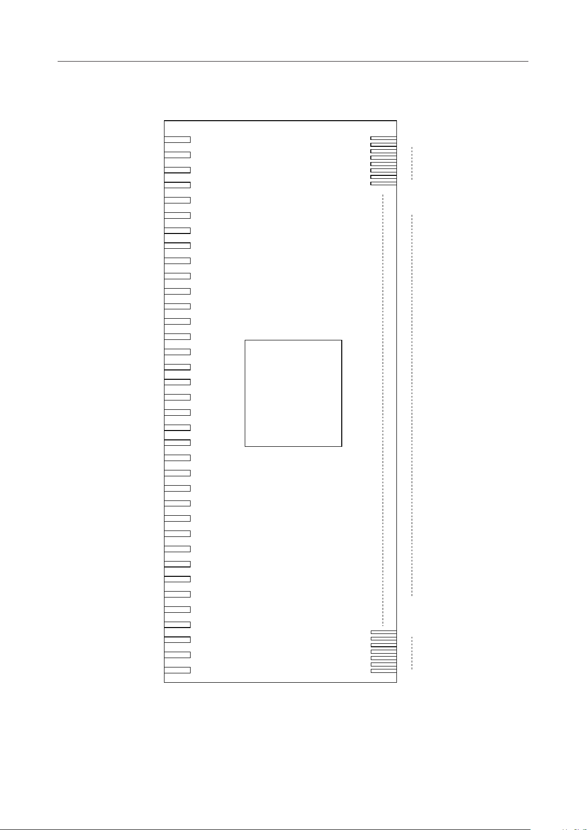
PIN CONFIGURATION
MSM9000B-xx
RESET
32K/EXT
9D/16D
P/S
XT
XT
V
SS
CS
C/D
RD
WR
SI
SHT
SO
DB7
DB6
DB5
DB4
DB3
DB2
DB1
DB0
V
DD
TEST
N1
N2
V
CC1
V
C1
V
SH
V
SS6
V
CC2
V
C2
V
SS1
V
SS2, 3
V
SS4
V
SS5
COM1
COM8
SEG1
SEG2
SEG59
SEG60
COM16
COM9
Pin Configuration Viewed From Pattern
3/38
¡ Semiconductor
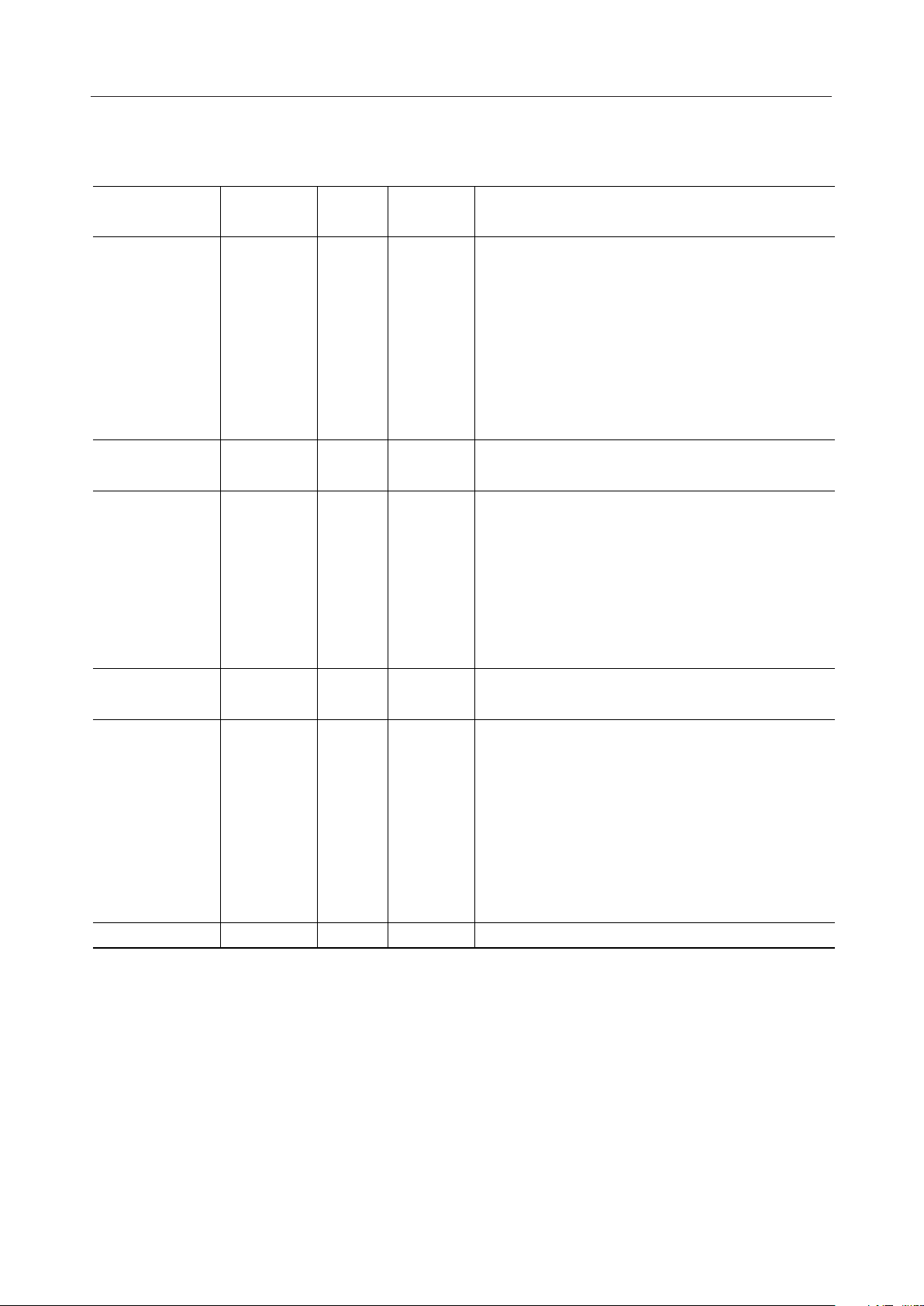
PIN DESCRIPTIONS
MSM9000B-xx
Function Type Description
Symbol
Number
of Pins
CPU Interface I Chip select input signal
Oscillation I Crystal oscillation input, clock input
Control Signal I Parallel/Serial interface switching signal input
CS
WR
RD
C/D
DB0-7
SI
SO
SHT
XT
XT
P/S
9D/16D
32K/EXT
RESET
1
1
1
1
8
1
1
1
I Write enable signal, latch for serial interface
I Read enable signal
Command/Data select input signalI
I/O 8-bit parallel data inputs/outputs
I Serial data input
O Serial data output
I Shift clock input for data input in serial interface mode
1
1
O Crystal oscillation output
1
1
1
1
I Duty select signal input
I Clock select signal input
I Reset is performed by setting the RESET input to "L"
level
N1, N2
TEST
LCD Driving
Output
Power Supply — Positive + power supply pin for LOGIC
SEG1-SEG60
COM1-COM16
V
DD
V
SS
V
, V
SS1
SS2, 3
V
, V
SS4
SS5
V
SS6
V
SH
VC1, V
CC1
VC2, V
CC2
60
16
2
1
I Contrast control signal input
I Test signal input. Fix to "L" Level or leave open
O Segment outputs for LCD driving
O Common outputs for LCD driving
1
1
4
1
1
2
2
— GND pin
— Boosted voltage output pins & bias power supply pins
— Voltage multiplier output pin (3-/2-fold)
— Haver output pin
— Voltage multiplier (3-/2-fold)
— Voltage multiplier (4-fold)
112Total
4/38
¡ Semiconductor
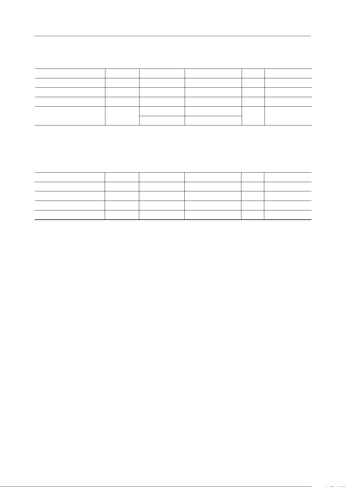
ABSOLUTE MAXIMUM RATINGS
MSM9000B-xx
Parameter Symbol Condition Rating Unit
Power supply voltage V
Bias voltage V
Input voltage V
DD
Ta=25°C, V
BI
I
Ta=25°C, VDD–V
DD–VSS
SS5
Ta=25°C V
–0.3 to +4.6
–0.3 to +7 V
–0.3 to VDD + 0.3
Applicable pin
V
V
, V
DD
SS
, V
V
DD
SS5
All input pins
Chip –55 to +150
Storage temperature
T
STG
TCP –30 to +85
°C
—
Ta: Ambient temperature
RECOMMENDED OPERATING CONDITIONS
Parameter Symbol Condition Range Unit
Power supply voltage V
Bias voltage V
IC source oscillation f
Operating temperature — –30 to +85T
DD
BI
int
op
*1 VDD is the highest pin and V
V
DD–VSS
*1, VDD–V
SS5
*2 kHz
the lowest for the bias voltage.
SS5
2.5 to 3.3
3 to 5.5 V
26 to 47
°C
*2 Connect the specified capacitors to the voltage doubler and LCD bias generator.
*3 Make sure that the crystal oscillation frequency or the divided clock frequency falls within
this range.
Applicable pin
V
, V
V
DD
V
DD, VSS5
*3
—
SS
Note 1: Ensure the chip is not exposed to any light.
Note 2: The bias voltage may exceed 5.5 V at some contrast stages. Adjust the stage with
software so that the bias voltage does not exceed 5.5 V.
5/38
¡ Semiconductor
MSM9000B-xx
ELECTRICAL CHARACTERISTICS
DC Characteristics (1)
(V
= 2.5 to 3.3 V, VBI = 3 to 5.5 V, Ta = –30 to +85°C)
DD
Parameter Symbol Condition Min. Typ. Max. Unit
Input high voltage 1 V
Input high voltage 2 V
Input low voltage 1 V
Input low voltage 2 V
Input high current 1
Input high current 2
Input low current 1
Off leakage current
Output high voltage 1
Output low voltage 1 V SO and DB0 to
COM output resistance
I
I
I
V
IH1
IH2
IL1
IL2
IH1
IH2
IL1
off
OH
OL1
C
S
—V
— 0.8V
–0.25 — V
DD
DD
—VDDV Other inputs
DD
— 0 — 0.55 V
— 0 — 0.2V
VI=V
VI=V
DD
DD
—— 1
10 — 60
VI=0 V –1 — —
/0 V –1 — 1
V
I=VDD
I
=–500 mA
O
IO=500 mAV
=±50 mAR
I
O
I
=±20 mAR
O
0.9V
DD
——
— — 0.1V
——10
——30SEG output resistance kW SEG1 to SEG60
DD
DD
During operation *1
Drain current 1
DD1
Crystal oscillation
—1535
f = 32.768 kHz
During operation *1
Drain current 2
I
DD2
External clock
—1535mA
f = 32 kHz
Applicable pin
XT
V
XT
V Other input pins
Input pins other
mA
than XT and TEST
TEST (pull-down
mA
resistor)
mA
Input pins other
than XT and TEST
SO and DB0 to
mAI
DB7
V
SO and DB0 to
DB7
DB7
kW COM1 to COM16
mAI
V
DD
V
DD
I
DD3
During standby
—— 7Drain current 3 mAV
*1 No output load
Note : The values in this table are assured when the chip is not exposed to light.
DD
6/38
¡ Semiconductor
MSM9000B-xx
DC Characteristics (2)
=0 V, VSS=–3 V, Ta=–30 to +85°C)
(V
DD
Parameter Symbol Condition Min. Typ. Max. Unit
Bias voltage 1 –V
SS1
–V
= "A"V 1/2A–0.1 1/2A 1/2A+0.1 V
SS2, 3
Applicable pin
V
N1 = "L", N2 = "L"
Bias voltages 2 and 3 –V
Bias voltage 4 –V
Bias voltage 5
Contrast pitch
–V
–V
SS2, 3
SS4
SS5
con
Contrast = "5"
–V
–V
= "A"V 3/2A–0.1 3/2A 3/2A+0.1 V V
SS2, 3
= "A"V 2A–0.2 2A 2A+0.2
SS2, 3
VBI for each stage 0.18 0.21 0.26
1.9 2.2 2.5 V V
V
V
V
Note 1: Connect a 0.1 µF capacitor to the LCD bias generator.
Note 2: The values in this table are assured when the chip is not exposed to light.
AC Characteristics
Parallel interface
(VDD=2.5 to 3.3 V, VBI=3 to 5.5 V, Ta=–30 to +85°C)
Parameter Symbol Condition Min.
RD high-level width t
WR high-level width t
WR low-level width —t
WR-RD high-level width —t
CS or C/D setup time —t
CS or C/D hold time —t
Write data setup time —t
Write data hold time —t
Read data output delay time CL=50 pFt
Read data hold time —t
External clock high-level width —t
External clock low-level width —t
RESET pulse width —t
Rise and fall time of external
clock
WRH
WRL
WWH
WWL
WWRH
AS
AH
DSW
DHW
DDR
DHR
WCH
WCL
WRE
, t
r
— 200
—RD low-level width t
200
— 200
200
200 — ns
50 — ns
0—ns
50 — ns
50 — ns
— 200 ns
20 — ns
1—ms
1—ms
2.0 — ms
f
—t
— 100 ns
Max.
—
—
—
—
SS1
SS2, 3
SS4
SS5
—
Unit
ns
ns
ns
ns
Note: The values in this table are assured when the chip is not exposed to light.
7/38

¡ Semiconductor
Serial interface
Parameter Symbol Condition Min.
CS or C/D setup time t
SI setup time t
SI hold time —t
SHT high-level pulse width —t
SHT low-level pulse width —t
SHT clock cycle time —t
SO ON delay time CL= 50 pFt
SO output delay time CL= 50 pFt
SO OFF delay time —t
BUSY delay time CL= 50 pFt
WR setup time —t
WR low-level pulse width —t
RESET pulse width —t
Rise and fall time of external
clock
SAS
SAH
IS
IH
WSHH
WSHL
SYS
ON
DS
OFF
BUSY
SHS
WWL
WRE
, t
r
MSM9000B-xx
(VDD = 2.5 to 3.3 V, VBI = 3 to 5.5 V, Ta = –30 to +85°C)
Max.
— 100
—CS or C/D hold time t
20
— 100
20
—
—
—
—
100 — ns
100 — ns
400 — ns
— 200 ns
0 200 ns
— 100 ns
— 200 ns
200 — ns
120 — ns
2.0 — ms
f
—t
— 100 ns
Unit
ns
ns
ns
ns
Note: The values in this table are assured when the chip is not exposed to light.
8/38
¡ Semiconductor
Timing Diagram for the Parallel Interface
—
V
CS
C/D
WR
IH
—
V
IL
—
V
IH
—
V
IL
t
AS
—
V
IH
—
V
IL
t
WRH
t
WWL
MSM9000B-xx
t
AH
t
WWH
t
WWRH
t
AS
t
WRL
t
AH
RD
DB0-7
RESET
XT
—
V
IH
—
V
IL
t
DSW
V
IH
V
IL
t
WRE
—
V
IL
t
r
—
V
IH
—
V
IL
t
DHW
t
f
t
WCL
t
DDR
V
OH
V
OL
t
WCH
t
DHR
V
IH
V
OH
= 0.8VDD,
= 0.9VDD,
V
V
= 0.2V
IL
OL
= 0.1V
DD
DD
9/38
¡ Semiconductor
Timing Diagram for the Serial Interface
—
V
CS
C/D
SI
SHT
IH
—
V
IL
—
V
IH
—
V
IL
—
V
IH
—
V
IL
t
SAS
—
V
IH
t
t
IS
IH
50%
—
V
IL
t
WSHL
t
WSHH
t
SHS
MSM9000B-xx
t
SAH
WR
SO
RESET
XT
—
V
IH
—
V
IL
t
ON
—
V
OH
V
OL
V
IL
"Z"
—
—
t
—
V
IH
—
V
IL
t
SYS
t
DS
t
WWLtBUSY
t
OFF
"Z"
t
WRE
t
r
f
V
= 0.8 VDD,
IH
V
= 0.2 V
IL
DD
V
OH
= 0.9 VDD,
V
OL
= 0.1 V
DD
10/38

¡ Semiconductor
MSM9000B-xx
FUNCTIONAL DESCRIPTION
Pin Functional Description
• CS (Chip Select)
Chip select input pin. A logic low on the CS input selects the chip and a logic high on the CS
input does not select the chip. Command and display data inputs can be enabled only when
the chip is selected.
When the input is high, the SO pin and DB0 to DB7 pins are in the high impedance state,
causing SHT, WR and RD pins high level internally.
• WR (Write Enable)
When the parallel interface is used, this pin is the write signal input. Data is written into the
register at the rising edge of WR pulse. When the serial interface is used, this pin is the latch
signal input. This pin is normally high.
• RD (Read Enable)
When the parallel interface is used, this pin is the read signal input. While the pulse is low,
data can be read. The pin is normally high. When this pin is made low with C/D set low, the
display data pointed to by the address pointer is output from DB0 to DB7. When the pin is
made low with C/D set high, busy data is output from DB0 and low signals are output from
DB1 to DB7. After the rising edge of WR, busy data (H) is output. The data automatically
changes to non-busy (L) after the specified time elapses.
When the serial interface is used, fix this pin to "H" or "L".
•C/D (Command/Data Select)
This input pin selects whether the data to be input to the SI pin and the DB7 to DB0 pins is
handled as a command or display data, depending on the state of the pin at the rising edge
of WR. When the pin is H, the input data is handled as a command. When the pin is L, display
data is input.
• DB0 to DB7 (Data Buses 0 to 7)
Data input and output pins for the parallel interface. Normally data buses 0 to 7 are in high
impedance, when RD is driven low, display data and the busy signal are output.
When the serial interface is used, leave this pin open.
• SI (Serial Data Input)
Data input pin for the serial interface. Commands and display data are read at the rising edge
of SHT and written to registers at the rising edge of WR. The eight-bit data immediately before
the rising edge of WR is valid.
When the parallel interface is used, fix this pin to "H" or "L".
• SO (Serial Data Output)
Data output pin for the serial interface. The display data pointed to by the address pointer is
output at the rising edge of SHT. After the rising edge of WR, busy data (H) is output.
The data automatically changes to non-busy (L) after the specified time elapses.
When the parallel interface is used, this pin remains in the high impedance state.
• SHT (Shift Clock)
Clock input pin to input and output serial interface data. Data input is synchronous with the
rising edge of the clock, and the data output is synchronous with the falling edge of the clock.
This pin is normally high.
When the parallel interface is used, fix this pin to "H" or "L".
11/38
¡ Semiconductor
MSM9000B-xx
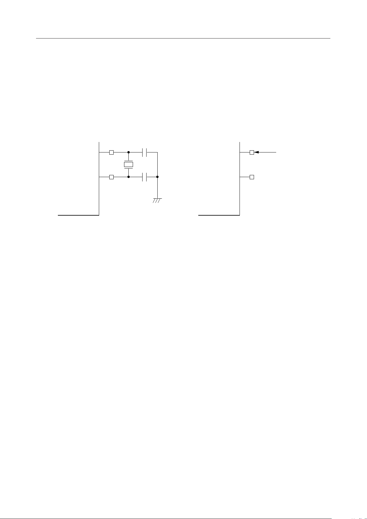
• XT (Crystal)
Input pin for crystal oscillation. By connecting a 32.768-kHz crystal and capacitors to this pin
and the XT pin, a crystal oscillation circuit is formed. When an external clock is used, input
the clock to the XT pin.
• XT (Crystal)
Output pin for crystal oscillation. By connecting a 32.768-kHz crystal and capacitors to this
pin and the XT pin, a crystal oscillation circuit is formed. When the external clock is used,
leave this pin open.
XT
18 pF
XT
18 pF
32.768 kHz
When forming a crystal oscillation circuit When inputting an external clock
XT
XT
External
clocks
OPEN
Oscillation circuit diagram
• P/S (Parallel/Serial Select)
Input pin to choose between the parallel interface and serial interface. To select the parallel
interface, make this pin low. To select the serial interface, make this pin high. After power
is turned on, do not change the setting of this pin.
• 9D/16D (Duty Select)
Input pin to set a duty cycle. When this pin is set to "H", a duty cycle of 1/9 is selected.
When the pin is set to "L", a duty cycle of 1/16 is selected. Choose either according to the panel
to be used. When a duty cycle of 1/9 is chosen, leave common output pins COM10 to COM16
open.
• 32K/EXT (Clock Select)
Input pin to choose crystal oscillation mode or external clock input mode. Leave this pin at
a "L" level.
• RESET (Reset)
Reset signal input pin. Setting this pin to L results in the initial state. For modes and the
display after a reset input, see "Mode Settings after a Reset Input".
• N1, N2 (Contrast Change)
Input pins that determine the voltages of V
SS2
and V
together with contrast adjustment by
SS3
a command. The table below shows the relationships between pin states and contrast
adjustment ranges.
12/38
 Loading...