


E2E1024-27-Y4
This version: Jan. 1998
MSM85C154HVS¡ Semiconductor
¡ Semiconductor
Previous version: Nov. 1996
MSM85C154HVS
MSM83C154S Piggy Back
GENERAL DESCRIPTION
The MSM85C154HVS is an 8-bit microcontroller that has been developed assuming that it is used
for evaluation of programs of MSM83C154S. ES (Engineering Sample) only.
FEATURES
• Operating range
Operating frequency : 1 to 22 MHz (16 to 22 MHz is recommended
for program development)
Operating voltage : 4.75 to 5.25 V (Use MSM85C154VS for 1 to 16
MHz)
Operating temperature : Room temperature
• Fully static circuit
• On-chip program memory : 16K ¥ 8-bit ROM (EPROM)
• On-chip data memory : 256 ¥ 8-bit RAM
• External program memory address space : 64 Kbytes
• External data memory address space : 64 Kbytes
• I/O port
(Port 1, 2, 3, impedance programmable) : 4 ports ¥ 8 bits
• 16-bit timer/counters : 3
• Multifunctional serial port : I/O Expansion mode
: UART mode (featuring error detection)
• 6-source 2-priority level
Interrupt and multi-level
Interrupt available by programming IP and IE registers
• Memory-mapped special function registers
• Bit addressable data memory and SFRs
• Minimum instruction cycle : 545 ns @ 22 MHz operation
• "Multiply"/"divide" instruction cycle : 2.18 ms @ 22 MHz operation
• Standby functions : Power-down mode (oscillator stop)
Activated by software or hardware; providing ports with floating or active status
The software power-down stet mode is terminated by interrupt signal enabling execution from the interrupted address.
• Package
40-pin ceramic Piggyback (ADIP40-C-600-2.54) (Product name: MSM85C154HVS)
1/15
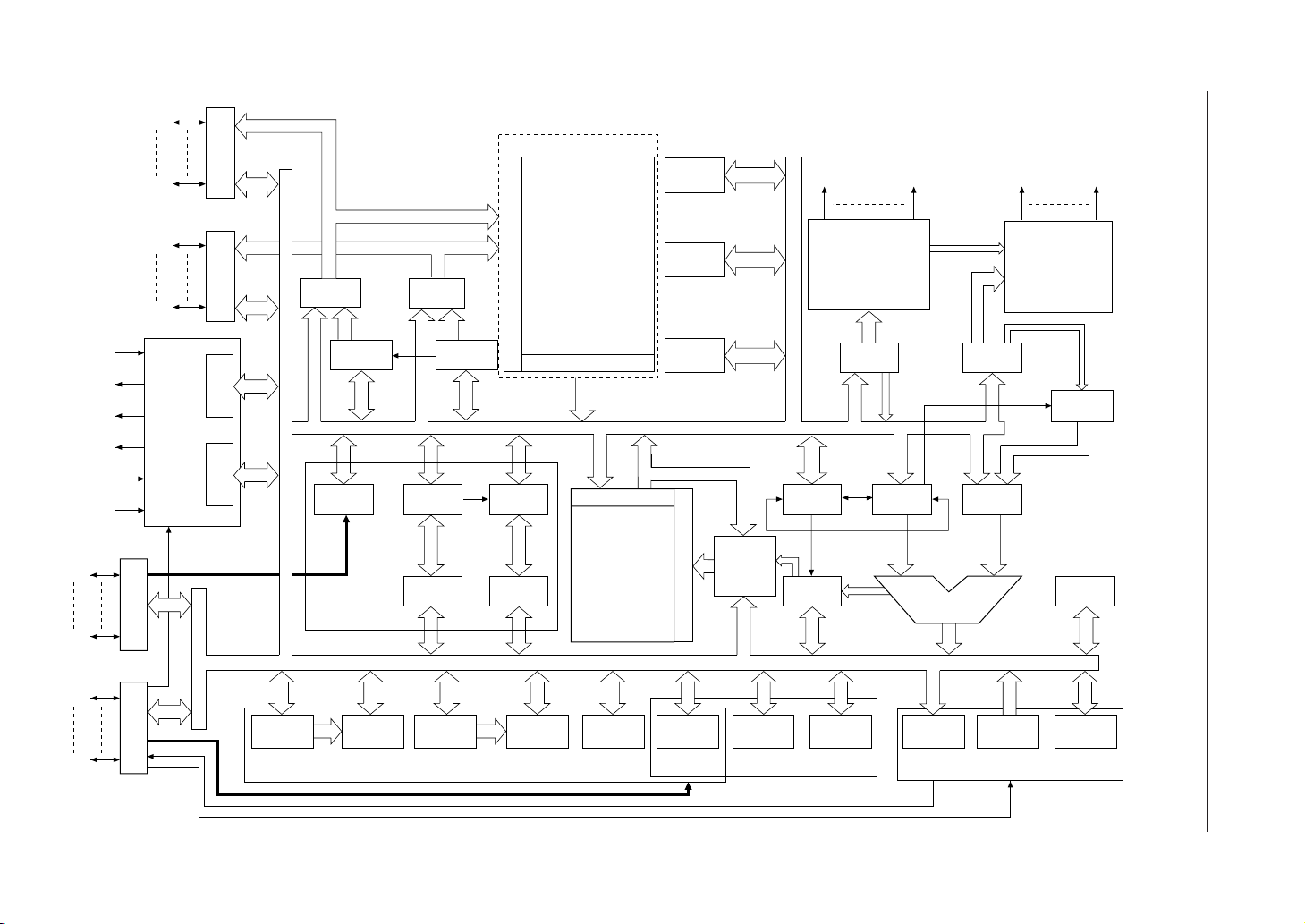
BLOCK DIAGRAM
P1.0
P1.7
XTAL1
XTAL2
ALE
PSEN
EA
RESET
P2.0
P2.7
P0.0
P0.7
OSC AND TIMING
PORT 1 PORT 3
PORT 2 PORT 0
PCON IOCON
PCHL
PCH
T2CON
TIMER/
COUNTER 2
PCLL
PCL
A0-A13
16K words ¥ 8 bits
TH2TL2
RCAP2H RCAP2L
SOCKET
EPROM
D0-7
R/W AMP
256 words
¥ 8 bits
DPH
DPL
SP
RAMDP
CONTROL SIGNAL
PLA
IR AIR
TR2ACC
PSW
SIGNALR/W
SPECIAL
FUNCTION
REGISTER
ADDRESS
DECODER
C-ROM
TR1
BR
ALU
2/15
P3.0
P3.7
TH1 TL1 TH0 TL0 TMOD TCON IE IP SBUF(T) SBUF(R)
TIMER/COUNTER 0 & 1
INTERRUPT
SERIAL IO
MSM85C154HVS¡ Semiconductor
SCON
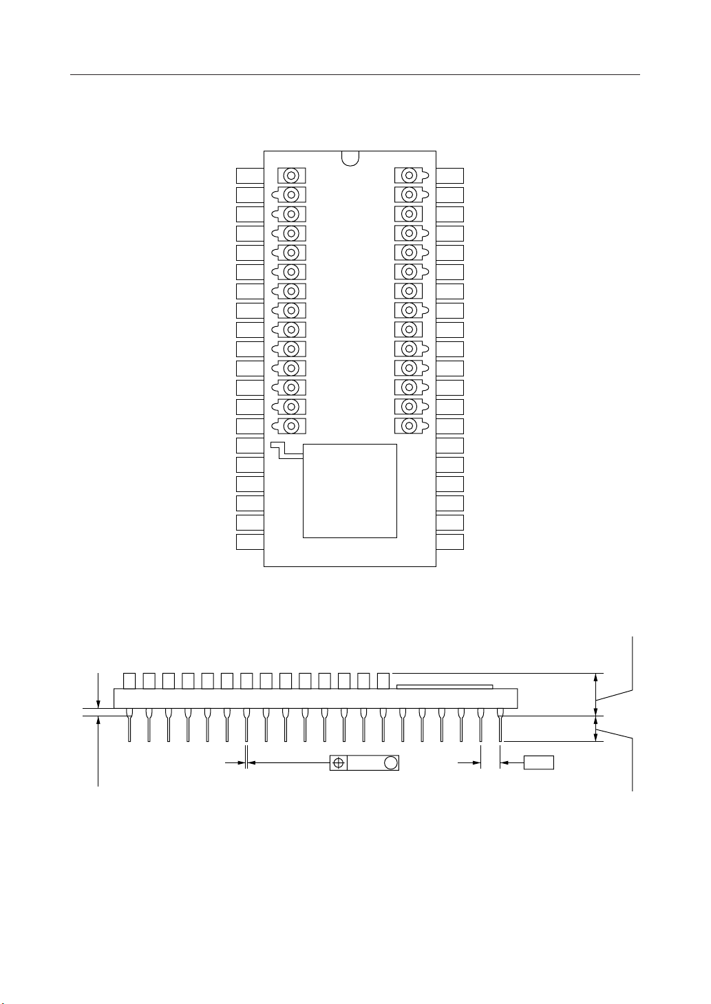
PIN CONFIGURATION (TOP VIEW)
MSM85C154HVS¡ Semiconductor
P1.0/T2
P1.1/T2EX
P1.2
P1.3
P1.4
P1.5
P1.6
P1.7
RESET
P3.0/RXD
P3.1/TXD
P3.2/INT0
P3.3/INT1
P3.4/T0
P3.5/T1/HPDI
P3.6/WR
P3.7/RD
XTAL2
XTAL1
V
1
2
3
4
5
6
7
8
9
10
11
12
13
14
VPP (VCC)
12
A
7
A
6
A
5
A
4
3
A
2
1
A
0
O
0
O
1
O
2
GND (VSS)
15
16
17
18
19
20
SS
V
CC
(V
) PGMA
CC
A
13
A
8
A
9
A
11
V
(OE)A
SS
A
10
CEA
O
7
O
6
O
5
O
4
O
3
40
39
38
37
36
35
34
33
32
31
30
29
28
27
26
25
24
23
22
21
V
CC
P0.0
P0.1
P0.2
P0.3
P0.4
P0.5
P0.6
P0.7
EA
ALE
PSEN
P2.7
P2.6
P2.5
P2.4
P2.3
P2.2
P2.1
P2.0
0.95MIN
0.46±0.10
f 0.25
M
40-Pin Package (Piggy back)
2.54
2.54MIN 7.6MAX
3/15

ABSOLUTE MAXIMUM RATINGS
Parameter Symbol Condition Rating Unit
Power Supply Voltage
Input Voltage
Storage Temperature
V
CC
V
I
T
STG
Ta=25°C –0.5 to 7 V
Ta=25°C –0.5 to VCC+0.5 V
— –55 to +150 °C
RECOMMENDED OPERATING CONDITIONS
Parameter Symbol Condition Range Unit
Power Supply Voltage
Oscillation Frequency
External Clock Operating
Frequency
Ambient Temperature
*1 Depends on the specification for crystal or ceramic resonator.
*1
V
CC
V
OSC
f
EXTCLK
See below. 4.75 to 5.25 V
See below. 1 to 22 MHz
See below. 0 to 22 MHz
Ta — room temp °C
MSM85C154HVS¡ Semiconductor
t
CY
(ms)
12
5
4
3
2
1
0.6
0.545
2.2
23456
4.75 5.25
Power Supply Voltage VCC (V)
1
3
6
12
20
22
f
OSC
f
EXTCLK
(MHz)
4/15

ELECTRICAL CHARACTERISTICS
DC Characteristics
Parameter Symbol Condition Min. Typ. Max. Unit
Input Low Voltage V
Input High Voltage V
Input High Voltage V
Output Low Voltage
(PORT 1, 2, 3)
Output Low Voltage
(PORT 0, ALE, PSEN)
Output High Voltage
(PORT 1, 2, 3)
Output High Voltage
(PORT 0, ALE, PSEN)
Logical 0 Input Current/
Logical 1 Output Current/
(PORT 1, 2, 3)
Logical 1 to 0 Transition
Current (PORT 1, 2, 3)
Input Leakage Current
(PORT 0 floating, EA)
RESET Pulldown Resistor R
Pin Capacitance C
Power Down Current I
IL
Except XTAL1, EA,
IH
XTAL1, RESET and EA 0.7 V
IH1
V
OL
V
OL1
V
OH
V
OH1
I
/ I
IL
OH
I
TL
I
LI
RST
VI=0.45V
Ta=25°C, f=1 MHz
IO
PD
(except XTAL1)
MSM85C154HVS¡ Semiconductor
=4.75 to 5.25V, VSS=0V, Ta=room temp)
(V
CC
Meas-
circuit
— –0.5 — V
0.2 V
+0.9 — V
and RESET
CC
CC
IOL=1.6 mA — — V
IOL=3.2 mA — — V
IOH=–60 mA
V
=5 V±10%
CC
=–30 mA 0.75 V
I
OH
=–10 mA 0.9 V
I
OH
IOH=–400 mA
V
=5 V±10%
CC
=–150 mA 0.75 V
I
OH
=–40 mA 0.9 V
I
OH
V
=0.45V
O
2.4 — V
CC
CC
2.4 — V
CC
CC
–5 –60 mA
VIL=2.0V — –240 mA
V
< VI < V
SS
CC
—— mA
—2040 kW
—— pF
——1 mA
0.2 VCC–0.1
V
+0.5
CC
—V
V
+0.5
CC
0.45
0.45
—
—V
—V
—
—
—
—V
—V
—
—
–80
–500
±10
125
10
50
uring
1
2
3
2
—
4
5/15

Maximum power supply current normal operation ICC (mA)
MSM85C154HVS¡ Semiconductor
V
CC
Freq
4.75V 5V 5.25V
2.2 3.1 4.11 MHz
3.9 5.2 7.03 MHz
15.0 16.0 17.012 MHz
19.0 20.0 22.016 MHz
25.0 27.0 29.022 MHz
Maximum power supply current idle mode ICC (mA)
V
CC
Freq
4.75V 5V 5.25V
0.8 1.2 1.61 MHz
1.2 1.7 2.33 MHz
4.1 4.4 4.812 MHz
5.1 5.5 6.016 MHz
6.5 7.0 7.522 MHz
Note: The values of Power-down current, operating current, and IDLE current do not include
the current dissipated by EPROM.
6/15

Measuring circuits
MSM85C154HVS¡ Semiconductor
1
V
CC
V
IH
(*3)
V
IL
INPUT
V
SS
(*2)
OUTPUT
V A
(*1)
I
O
V
A
3
2
V
CC
INPUT
V
SS
4
OUTPUT
A
V
CC
V
IH
(*3)
V
IL
INPUT
V
SS
(*2)
OUTPUT
V A
V
CC
V
IH
(*3)
V
IL
INPUT
OUTPUT
V
SS
*1: Repeated for specified input pins.
*2: Repeated for specified output pins.
*3: Input logic for specified status.
7/15

AC Characteristics
External program memory access AC characteristics
= 4.75 to 5.25V, VSS = 0V, Ta = room temp
V
CC
PORT 0, ALE, and PSEN connected with 100 pF load, other connected with 80 pF load
Variable clock from
Parameter Symble Unit
Min. Max.
XTAL1, XTAL 2 Oscillation Cycle
ALE Signal Width
Address Setup Time
(to ALE Falling Edge)
Address Hold Time
(from ALE Falling Edge)
Instruction Data Read Time
(from ALE Falling Edge)
From ALE Falling Edge to PSEN
Falling Edge
PSEN Signal Width
Instruction Data Read Time
(from PSEN Falling Edge)
Instruction Data Hold Time
(from PSEN Rising Edge)
Bus Floating Time after Instruction
Data Read (from PSEN Rising Edge)
Instruction Data Read Time
(from Address Output)
Bus Floating Time(PSEN Rising
Edge from Address float)
Address Output Time from PSEN
Rising Edge
t
CLCL
t
LHLL
t
AVLL
t
LLAX
t
LLPL
t
LLPL
t
PLPH
t
PLIV
t
PXIX
t
PXIZ
t
AVIV
t
AZPL
t
PXAV
45.5 1000 ns
2t
CLCL
1t
CLCL
1t
CLCL
1t
CLCL
3t
CLCL
1t
CLCL
*1 The variable check is from 0 to 22 MHz when the external check is used.
1 to 22 MHz
-40 — ns
-15 — ns
-35 — ns
—4t
-30 — ns
-35 — ns
—3t
0—ns
—1t
—5t
0—ns
-20 — ns
MSM85C154HVS¡ Semiconductor
*1
-100 ns
CLCL
-45 ns
CLCL
-20 ns
CLCL
-105 ns
CLCL
8/15

External program memory read cycle
t
LHLL
ALE
MSM85C154HVS¡ Semiconductor
PSEN
PORT2
t
AVLLtLLPL
t
LLAXtAZPL
A0 to A7
t
AVIV
t
LLIV
t
PLIV
t
PLPH
t
PXIX
INSTR
IN
t
PXIZ
t
PXAV
A0 to A7PORT0
A8 to A15 A8 to A15 A8 to A15
9/15

External data memory access AC characteristics
= 4.75 to 5.25V, VSS = 0V, Ta = room temp
V
CC
PORT 0, ALE, and PSEN connected with 100 pF load, other connected with 80 pF load
Variable clock from
Parameter Symble Unit
1 to 22 MHz
Min. Max.
XTAL1, XTAL2 Oscillator Cycle
ALE Signal Width
Address Setup Time
(to ALE Falling Edge)
Address Hold Time
(from ALE Falling Edge)
RD Signal Width
WR Signal Width
RAM Data Read Time
(from RD Signal Falling Edge)
RAM Data Read Hold Time
(from RD Signal Rising Edge)
Data Bus Floating Time
(from RD Signal Rising Edge)
RAM Data Read Time
(from ALE Signal Falling Edge)
RAM Data Read Time
(from Address Output)
RD/WR Output Time from ALE
Falling Edge
RD/WR Output Time from Address
Output
WR Output Time from Data Output
Time from Data to WR Rising Edge
Data Hold Time
(from WR Rising Edge)
Time from to Address Float RD
Output
Time from RD/WR Rising Edge to
ALE Rising Edge
t
CLCL
t
LHLL
t
AVLL
t
LLAX
t
RLRL
t
WLWH
t
RLDV
t
RHDX
t
RHDZ
t
LLDV
t
AVDV
t
LLWL
t
AVWL
t
QVWX
t
QVWH
t
WHQX
t
RLAZ
t
WHLH
45.5 1000 ns
2t
CLCL
1t
CLCL
1t
CLCL
6t
CLCL
6t
CLCL
—5t
—2t
—8t
—9t
3t
CLCL
4t
CLCL
2t
CLCL
7t
CLCL
2t
CLCL
1t
CLCL
-40 — ns
-15 — ns
-35 — ns
-100 — ns
-100 — ns
CLCL
0—ns
CLCL
CLCL
-40 3t
-70 — ns
-40 — ns
-105 — ns
-50 — ns
0—ns
-30 1t
*1 The variable check is from 0 to 22 MHz when the external check is used.
MSM85C154HVS¡ Semiconductor
*1
-105 ns
-70 ns
CLCL
-100 ns
-105 ns
+40 ns
CLCL
+40 ns
CLCL
10/15

External data memory read cycle
ALE
PSEN
RD
PORT 0
INSTR
IN
A0 to A7
PCL
t
LHLL
t
AVLL
A0 to A7
Rr or DPL
t
LLAX
t
AVWL
t
LLWL
t
AZRL
t
LLDV
t
AVDV
t
RLDV
t
RLRH
t
RHDX
DATA IN
MSM85C154HVS¡ Semiconductor
t
WHLH
t
RHDZ
A0 to A7
PCL
PORT 2
PCH A8 to A15 PCH P2.0 to P2.7 DATA A8 to A15 DPHor A8 to A15 PCH
External data memory write cycle
ALE
PSEN
WR
PORT 0
PORT 2
INSTR
IN
A8 to A15
PCH
A0 to A7
PCL
A8 to A15 PCH P2.0 to P2.7 DATA A8 to A15 DPHor A8 to A15 PCH
t
LHLL
t
AVLL
A0 to A7
Rr or DPL
t
t
AVWL
t
LLWL
LLAX
t
QVWX
t
WLWH
t
QVWH
DATA (ACC)
t
WHLH
t
WHQX
A0 to A7
PCL
11/15

Serial port (I/O extension mode) AC characteristics
Parameter Symbol Min. Max. Unit
Serial Port Clock Cycle Time t
Output Data Setup to Clock Rising Edge t
Output Data Hold After Clock Rising Edge t
Input Data Hold After Clock Rising Edge t
Clock Rising Edge to Input Data Valid t
XLXL
QVXH
XHQX
XHDX
XHDV
10t
2t
MSM85C154HVS¡ Semiconductor
= 4.75 to 5.25V, VSS = 0V, Ta = room temp)
(V
CC
12t
CLCL
-133 —
CLCL
-75 —
CLCL
0—
— 10t
—ns
-133
CLCL
ns
ns
ns
ns
12/15

MACHINE
CYCLE
ALE
SHIFT
CLOCK
t
XLXL
13/15
OUTPUT
DATA
INPUT
DATA
t
QVXH
VALID VALID VALID VALID VALID VALID VALID VALID
t
XHDV
t
XHQX
t
XHDX
MSM85C154HVS¡ Semiconductor

AC characteristics measuring conditions
1.Input/output signal
MSM85C154HVS¡ Semiconductor
V
OH
V
IH
V
IH
V
OH
TEST POINT
V
V
OL
IL
* The input signals in AC test mode are either VOH (logic "1") or V
V
IL
V
OL
(logic "0") input signals
OL
where logic "1" corresponds to a CPU output signal waveform measuring point in excess of
VIH, and logic "0" to a point below VIL.
2.Floating
V
OH
V
OL
V
IH
V
IL
Floating
V
V
IH
V
IL
OH
V
OL
* The port 0 floating interval is measured from the time the port 0 pin voltage drops below V
after sinking to GND at 2.4 mA when switching to floating status from a "1" output, and from
the time the port 0 pin voltage exceeds VIL after connecting to a 400 mA source when switching
to floating status from a "0" output.
XTAL1 external clock input waveform conditions
Parameter Symbol Min. Max. Unit
External Clock Freq. 1/t
Clock Pulse width 1 t
Clock Pulse width 2 t
Rise Time t
Fall Time t
CLCL
CHCx
CLCX
CLCH
CHCL
0 22 MHz
15 —
15 —
—5
—5
ns
ns
ns
ns
IH
External clock drive waveform
- 0.5
V
CC
0.45 V
EXTERNAL
OSCILLATOR
SIGNAL
0.7V
CC
0.2VCC - 0.1
t
CHCL
t
CLCX
NC
t
CLCH
t
CLCL
XTAL2
XTAL1
V
SS
t
CHCX
14/15
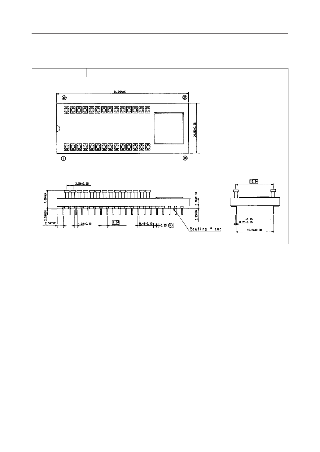
PACKAGE DIMENSIONS
ADIP40-C-600-2.54
MSM85C154HVS¡ Semiconductor
(Unit : mm)
Notes for Mounting the Surface Mount Type Package
The SOP, QFP, TSOP, SOJ, QFJ (PLCC), SHP and BGA are surface mount type packages, which
are very susceptible to heat in reflow mounting and humidity absorbed in storage.
Therefore, before you perform reflow mounting, contact Oki’s responsible sales person for the
product name, package name, pin number, package code and desired mounting conditions
(reflow method, temperature and times).
15/15
 Loading...