OKI MSM6782-01MS-K, MSM6782-01RS Datasheet

¡ SemiconductorMSM6782-01
¡ Semiconductor
MSM6782-01
REAL TIME CLOCK
GENERAL DESCRIPTION
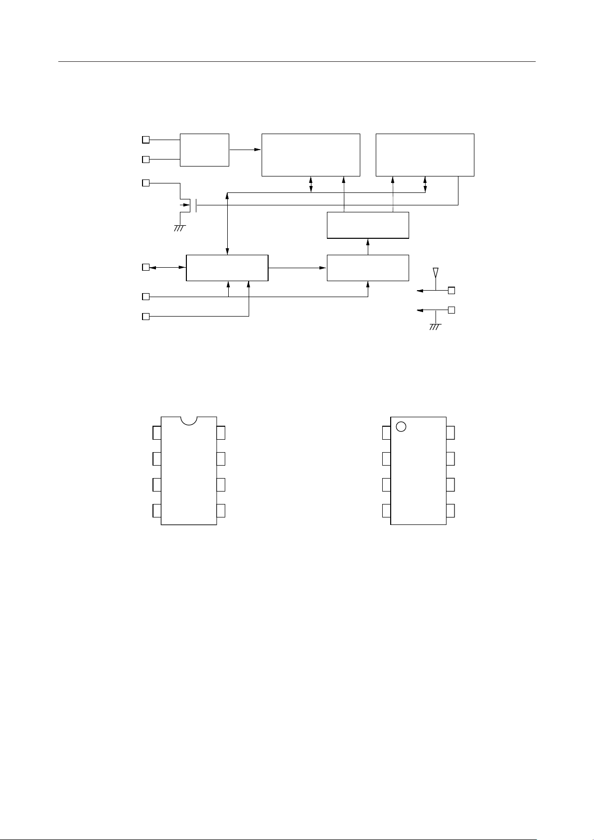
The MSM6782 - 01 is a CMOS Serial Interface Real Time Clock/Calendar.
The serial interface that can be controlled by mere 3 signal lines has minimized the number of
CPU terminals required .
The MSM6782 - 01 provides 30-second adjustment, oscillation stop detection, and periodic flag
setting and signal output in 4 diferent cycle periods.
The clock ranges are seconds, minutes, hours, days, months, years, and days of the week.
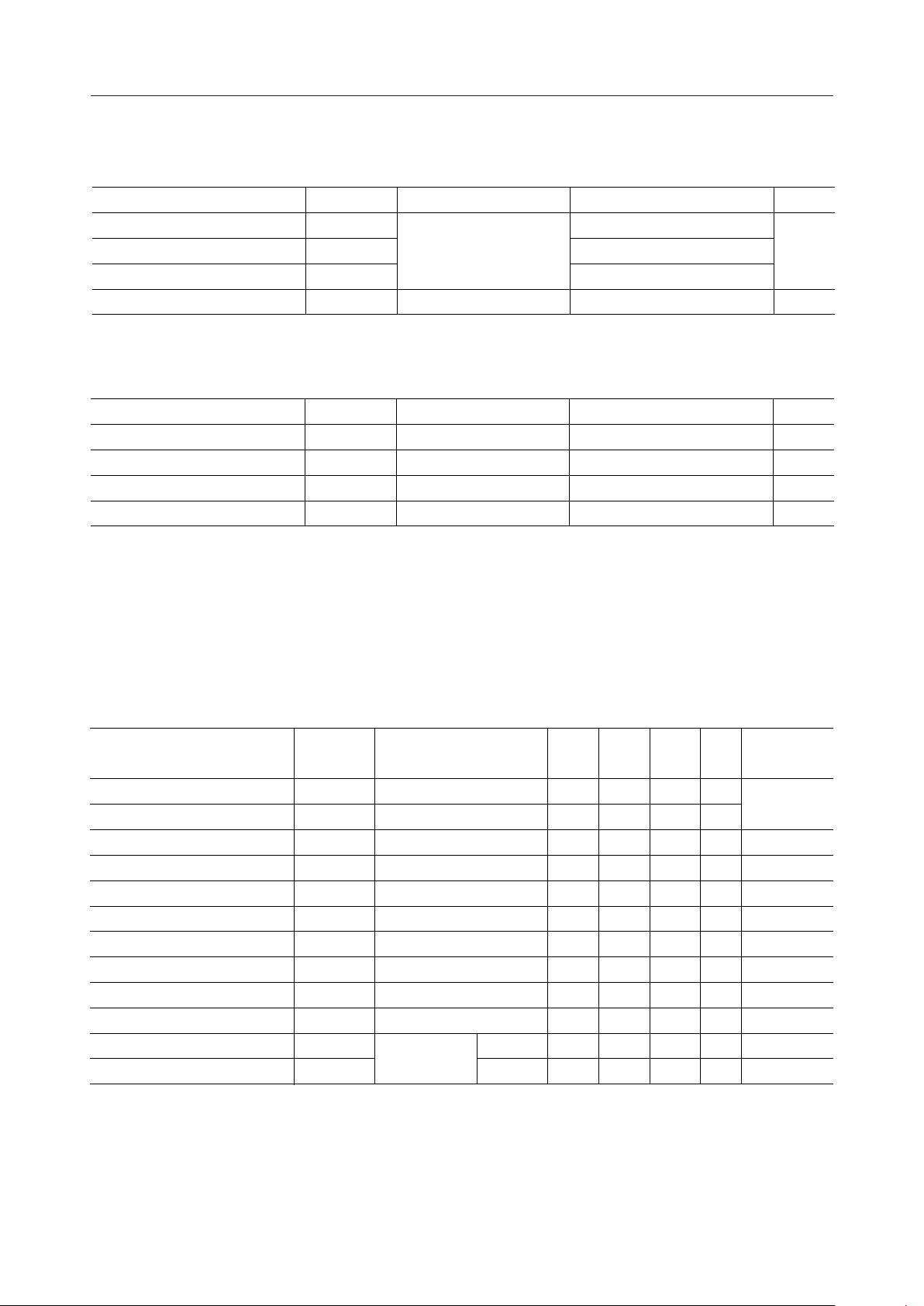
The interface supply voltage is 2.7V to 5.5V and the clock supply voltage is 2.0V to 5.5V.
The MSM6782 - 01 comes in an 8-pin DIP package or an 8-pin SOP package.
The MSM6782 - 01 is highly integrated and is suitable for use in a variety of portable applications.
FEATURES
• Real time clock providing seconds, minutes, hours, days, months, and days of the week.
• Serial interface controlled by 3 signal lines
• A periodic interrupt output in 4 different cycle periods (or periodic waveform output)
• Automatic leap year calendar
• 30-second adjustment controlled by software
• Stop and restart of clock
• Wide range of interface power supply: 2.7V to 5.5V
• Wide range of clock power supply: 2.0V to 5.5V
• 32.768kHz external quart crystal
• Low current consumption
• 8-pin plastic DIP (DIP8-P-300) (MSM6782-01RS)
• 8-pin plastic SOP (SOP8-P-250-K) (MSM6782-01MS-K)
120
BLOCK DIAGRAM
MSM6782-01¡ Semiconductor
XT
XT
STD.P
DATA I/O
CLK
CE
PIN CONFIGURATION
OSC
Data buffer
Clock/calendar
registers
Control registers
Decoder
Address counter
(C
D
, CE, CF)
V
DD
V
SS
8
STD.P
DATA I/O
Note : Note :
1
2
3
CLK
4
CE
The actual type name is displayed
V
DD
7
XT
6
XT
5
V
SS
STD.P
DATA I/O
as 6782-01.
8
V
DD
7
XT
6
XT
5
V
SS
CLK
CE
1
2
3
4
8-Pin Plastic SOP8-Pin Plastic DIP
The actual type name is displayed
as 82-01.
121
¡ SemiconductorMSM6782-01
PIN DESCRIPTION
• STD.P (Pin No. 1)
Periodic output of N-CH OPEN DRAIN type or interrupt signal output of N-CH OPEN
DRAIN type for the CPU. The periodic output is used to check the reference signal and
oscillation frequency.
This pin is set as periodic output or interrupt signal output by writing “1” or “0” to the INT/
STND bit.
This output is not inhibited by CE. For more information, see “FUNCTIONAL DESCRIPTION OF REGISTERS”.
• DATA I/O (Pin No.2)
Input/output pin for setting of WRITE mode or READ mode, writing of addresses, or
writing/reading of data.
This pin is used as an input or output pin in high impedance state depending on whether
WRITE mode or READ mode is selected in the first 8-bit data cycle after the rising of the CE
input pulse.
• CLK (Pin No. 3)
Shift clock input pin. Data is taken in on the rising edge of a shift clock pulse when in WRITE
mode and data is output when in READ mode.
• CE (Pin No. 4)
Chip enable input pin. “H” level on this pin means “enable”.
When this pin is low, the DATA I/O pin goes into high impedance state, and DATA I/O and
CLK are disabled inside the LSI and current stops flowing through those pins.
“L” level on this pin forces the TEST and REST bits of the CF registers and the fr flag to be set
to “0”.
When turning the power ON, set this pin to “L” level.
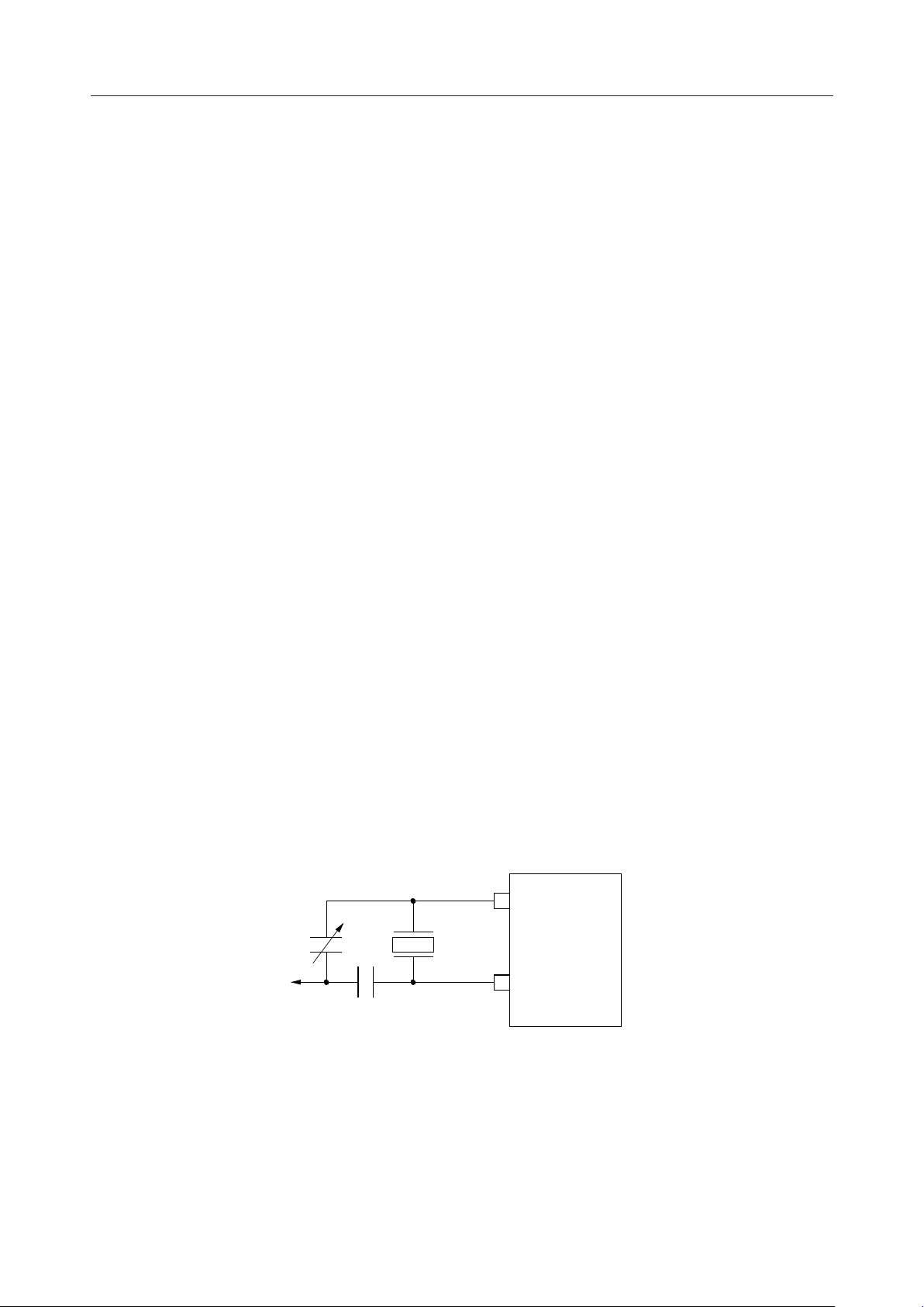
• XT, XT (Pin Nos. 7 and 6)
32.768kHz crystal is to be connected to these pins.
XT
C
1
V
DD
MSM6782-01XT
XT
C
2
When an external clock is used, it is to be input from XT, while XT should be left open.
The oscillation crystal and capacitors should be placed as close to the IC as possible.
The oscillation circuit and other signal lines on any side of the LSI should be distant from each
other.
•VDD, VSS (Pin No.5)
Power supply pins. VDD is used for positive supply and VSS is for negative supply.
122
ABSOLUTE MAXIMUM RATINGS
Parameter Symbol UnitRatingCondition
T
V
DD
V
V
STG
I
O
Ta = 25°C
—
Power supply voltage
Input voltage
Output voltage
Storage temperature
RECOMMENDED OPERATING CONDITIONS
Parameter Symbol UnitRatingCondition
Power supply voltage
Clock power supply
Crystal frequency
Operating temperature
V
DD
V
CLK
f
X
T
OP
—V
—
—
—
–0.3 to 7.0
–0.3 to VDD+0.3
V
ss
–0.3 to VDD+0.3
V
ss
–55 to +150
2.7 to 5.5
2.0 to 5.5
32.768
–40 to +85
MSM6782-01¡ Semiconductor
V
°C
V
kHz
°C
(Note) Clock power supply : Crystal oscillation and clock must be assured
ELECTRICAL CHARACTERISTICS
DC Characteristics
(VDD = 2.7 to 5.5.V, Ta = –40 to +85°C)
Parameter Symbol
"H" Input Voltage
"L" Input Voltage
"H" Input Current (1)
"L" Input Current (1)
"H" Input Current (2)
"L" Input Current (2)
"L" Output Current (1)
"H" Output Current
"L" Output Current (2)
OFF Leak Current
Current Consumption(1)
Current Consumption(2)
V
V
V
V
V
V
V
I
IH1
I
IL1
I
IH2
I
IL2
OL1
V
OH
OL2
OFLK
DD1
DD2
IH
IL
VI=V
DD
VI=V
SS
VI=V
DD
VI=V
SS
—
—
IO=1.0mA
=–400mA
I
O
=1.0mA
I
O
V
O=VDD
fX=32.768kHz
V
(CE)=0V
I
VDD=5V
VDD=2V
MINCondition
0.8V
0.8V
TYP MAX Unit
—
DD
—
—
—
—
—
—
—
—
DD
—
—
—
—
—
—
—
—
—
0.2V
–10
0.2V
0.2V
10.0
— — 20.0 mAV
—
—
2.5
—
–1
10
—
Applicable
terminal
V
All input pins
except XT
V
DD
1
mA
mA
mA
mA
DD
DD
mA
mA
V
V
V
CE, CLK
CE, CLK
DATA I/O
DATA I/O
DATA I/O
DATA I/O
STD.P
STD.P
DD
V
DD
123
• AC Characteristics
Parameter Symbol MINCondition
CLK "H" Pulse Width
CLK "L" Pulse Width
CE Setup Time
CE Hold Time
CE Recovery Time
CLK Setup Time
CLK Hold Time
WRITE Data Setup Time
WRITE Data Hold Time
READ Data Delay Time
Output Disable Delay Time
Input Rise, Fall Time
t
t
t
t
t
t
CKS
t
CKH
t
t
t
t
t
WH
WL
CS
CH
CR
DS
DH
RD
RZ
RF
= 50pF
C
L
—
—
—
—
—
—
—
—
—
—
—
¡ SemiconductorMSM6782-01
(VDD = 2.7 to 5.5V, Ta = –40 to +85°C)
TYP MAX Unit
300
300
150
200
300
20
20
50
50
—
— — 100
—
—
—
—
—
—
—
—
—
—
—
—
—
—
—
—
—
—
—
—
—
250
20
ns
ns
ns
ns
ns
ns
ns
ns
ns
ns
ns
ns
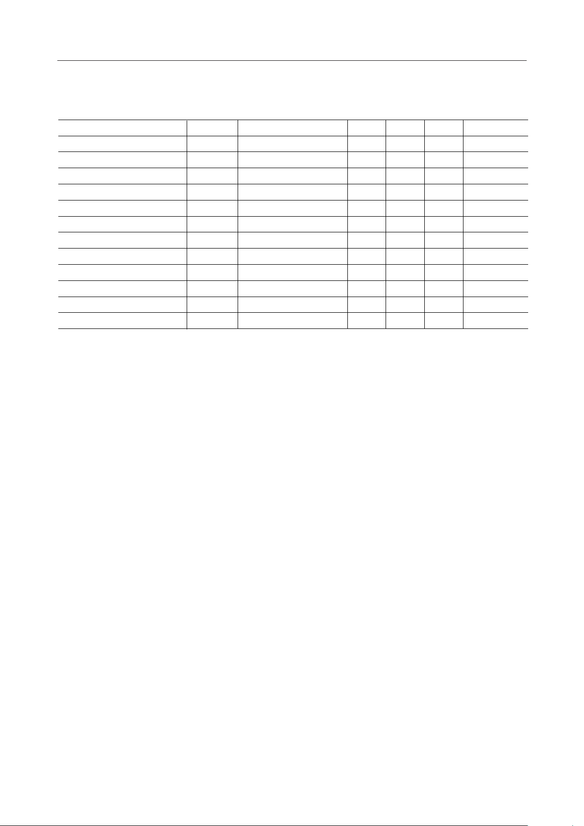
(Note) See Timing Chart.
124
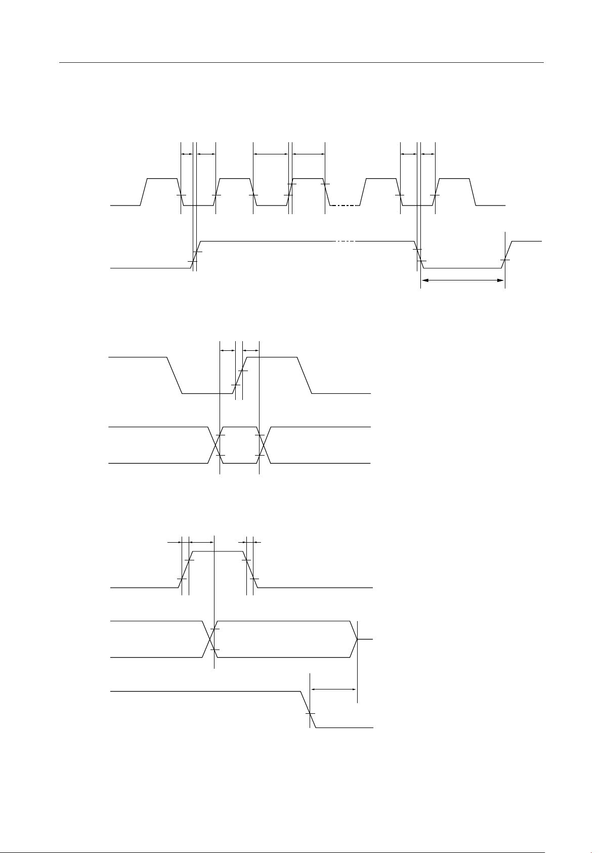
TIMING CHART
MSM6782-01¡ Semiconductor
CLK
CE
WRITE mode
CLK
t
CKS
V
IL
V
IH
V
IL
t
CS
V
t
DS
V
IL
t
WL
IL
t
DH
V
IH
t
WH
V
IH
V
V
IH
IL
t
V
IL
CH
t
CKH
V
IL
V
IH
V
IL
t
CR
V
IL
DATA I/O
READ mode
CLK
DATA I/O
CE
V
IH
V
IL
tRFt
RD
V
IH
V
IL
V
IH
V
IL
V
OH
V
OL1
V
IH
V
IL
t
RF
HiZ
t
RZ
V
IL
125
 Loading...