OKI MSM6775TS-K Datasheet

E2B0012-27-Y2
¡ Semiconductor MSM6775
¡ Semiconductor
This version: Nov. 1997
Previous version: Mar. 1996
MSM6775
1/3, 1/4, 1/5 DUTY LCD DRIVER WITH 5-DOT COMMON DRIVER AND 80-DOT
SEGMENT DRIVER
GENERAL DESCRIPTION
The MSM6775 is an LCD driver for dynamic display providing 3-duty-switchable pins (1/3, 1/
4 and 1/5 duty). It can directly drive LCDs of up to 400, 320 and 240 segments when 1/5, 1/4
and 1/3 duty are selected, respectively.
FEATURES
• Operating range
Supply voltage (VDD) : 2.7 to 5.5V
Operating temperature (T
LCD driving voltage (VDD-V
• Segment output : 80 pins
1/5 duty : Up to 400 segments can be displayed.
1/4 duty : Up to 320 segments can be displayed.
1/3 duty : Up to 240 segments can be displayed.
• Serial transfer clock frequency : 4MHz
• Serial interface with CPU : Through three input pins (DATA, LOAD, and
• One-to-one corresponcence between input data and its output
When input data is at "H" level : Display goes on.
When input data is at "L" level : Display goes off.
• Built-in oscillator circuit for COMMON signals
• The entire display can be turned off. (BLANK pin)
• Package:
100-pin plastic TQFP (TQFP100-P-1414-0.50-K) (Product name : MSM6775TS-K)
) : –40 to +85°C
op
) : 3.5 to 5.5V
LC3
CLOCK)
1/13

¡ Semiconductor MSM6775
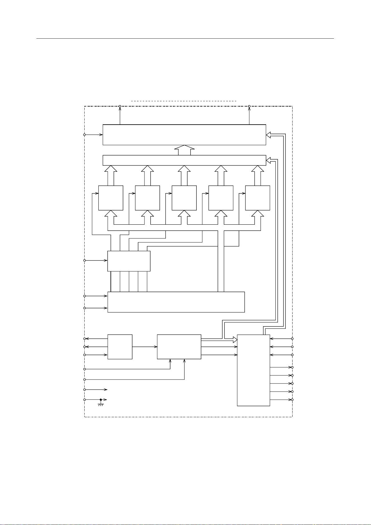
BLOCK DIAGRAM
SEG1 SEG80
BLANK
LOAD
DATA
CLOCK
80-BIT
LATCH 5
SELECTOR
LATCH
80-DOT SEGMENT DRIVER
80-CH DATA SELECTOR
80-BIT
LATCH 4
80-BIT
LATCH 3
88-BIT SHIFT REGISTER
80-BIT
LATCH 2
80-BIT
LATCH 1
80
OSC–R
OSC–C
OSC–IN
DSEL1
DSEL2
V
DD
V
SS
OSC
TIMING
GENERATOR
COMMON
DRIVER
V
LC1
V
LC2
V
LC3
COM1
COM2
COM3
COM4
COM5
2/13

¡ Semiconductor MSM6775
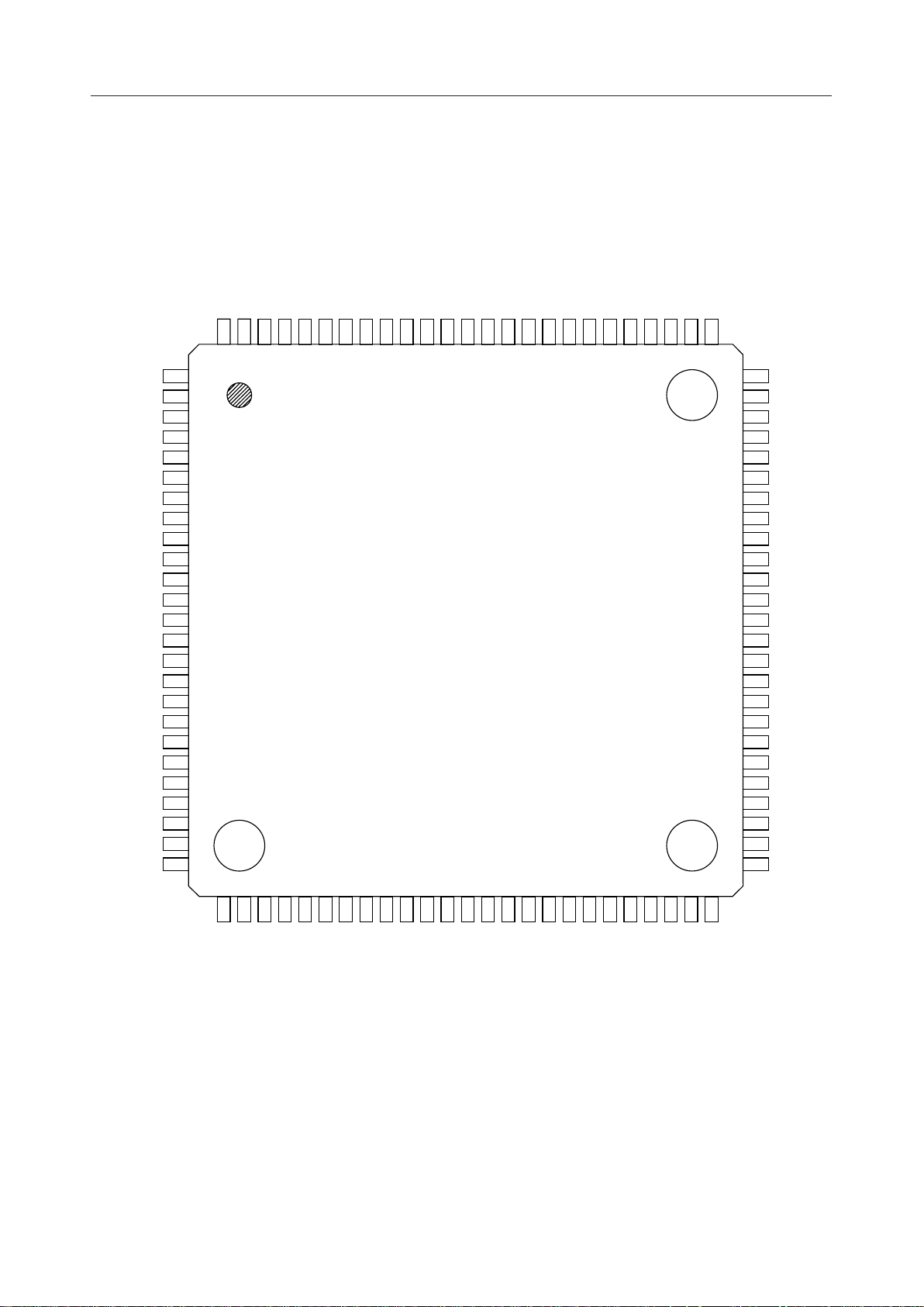
PIN CONFIGURATION (TOP VIEW)
SEG26
SEG27
SEG28
SEG29
SEG30
SEG31
SEG32
SEG33
SEG34
SEG35
SEG36
SEG37
SEG38
SEG39
SEG40
SEG41
SEG42
SEG43
SEG44
SEG45
SEG46
SEG47
SEG48
SEG49
SEG50
76
77
78
79
80
81
82
83
84
85
86
87
88
89
90
91
92
93
94
95
96
97
98
99
100
SEG51
1
2SEG52
3SEG53
4SEG54
5SEG55
6SEG56
7SEG57
8SEG58
9SEG59
10SEG60
11SEG61
12SEG62
13SEG63
14SEG64
15SEG65
16SEG66
17SEG67
18SEG68
19SEG69
20SEG70
21SEG71
22SEG72
23SEG73
24SEG74
25SEG75
75
74
73
72
71
70
69
68
67
66
65
64
63
62
61
60
59
58
57
56
55
54
53
52
51
SEG25
SEG24
SEG23
SEG22
SEG21
SEG20
SEG19
SEG18
SEG17
SEG16
SEG15
SEG14
SEG13
SEG12
SEG11
SEG10
SEG9
SEG8
SEG7
SEG6
SEG5
SEG4
SEG3
SEG2
SEG1
26
27
SEG77
SEG76
29
28
SEG79
SEG78
31
30
NC
SEG80
39
38
37
36
35
34
33
32
DD
V
LOAD
DATA
CLOCK
DSEL2
BLANK
OSC-R
DSEL1
NC : No connection
100-Pin Plastic TQFP
40
OSC-C
42
41
SS
V
OSC-IN
43
V
LC3
44
V
LC2
45
V
LC1
46
COM5
47
COM4
48
COM3
49
COM2
50
COM1
3/13

¡ Semiconductor MSM6775
PIN DESCRIPTIONS
Symbol Type
OSC-IN I
OSC-C O
OSC-R O
DATA I
CLOCK I
LOAD I
BLANK I
DSEL1 I
DSEL2 I
Description
Pins for oscillation. The oscillator circuit is configured by externally connecting two
resistors and a capacitor. Make the wiring length as short as possible, because the
resistor connected to the OSC-IN pin has a higher value and the circuit is susceptible
to external noise.
Serial data input pin. The display goes on when input data is at "H" level, and it goes
off when input data is at "L" level.
Shift clock input pin. Data from the DATA pin is transferred in synchronization with the
rising edge of the shift clock. (Built-in Schmitt circuit is used.)
Load signal input pin. Serially input data is transferred to the 80-bit latch at "H" level
of this load signal, then held at "L" level.
Input pin that turns off all segments. The entire display goes off when "L" level is
applied to this pin. The display returns to the previous state when "H" level is applied.
Input pins to select 1/3, 1/4, or 1/5 duty. Following shows how each duty is selected.
DSEL2 DSEL1
L
L
H
L
H
X
Duty selected
1/3
1/4
1/5
X: Don't care
COM1 to
COM5
SEG1 to
SEG80
V
LC1
V
LC2
V
LC3
V
DD
V
SS
O
O
—
—
Display output pins for LCD. These pins are connected to the COMMON side on the
LCD panel.
Display output pins for LCD. These pins are connected to the SEGMENT side on the
LCD panel. For the correspondence between the output of these pins and input data,
see Section, "Data Structure".
Bias pins for LCD drive. Through these pins, bias voltages for the LCD
are externally supplied. The bias potential must meet the following condition:
V
DD>VLC1≥VLC2>VLC3
Supply voltage pin and ground pin.
4/13
 Loading...