OKI MSM58321 Datasheet
¡ Semiconductor MSM58321
¡ Semiconductor
MSM58321
REAL TIME CLOCK/CALENDAR
DESCRIPTION
The MSM 58321 is a metal gate CMOS Real
Time Clock/Calendar with a battery backup
function for use in bus-oriented microprocessor applications.
The 4-bit bidirectional bus line method is used
for the data I/O circuit; the clock is set, corrected, or read by accessing the memory.
FEATURES
• 7 Function-Second, Minute, Hour, Day,
Day-of-Week, Month, Year
• Automatic leap year calender
• 12/24 hour format
• Frequency divider 5-poststage reset
• Reference signal output
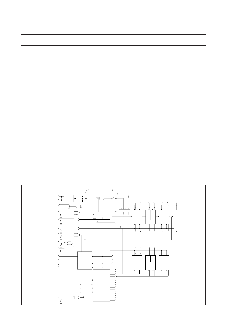
FUNCTIONAL BLOCK DIAGRAM
5-poststage (O
11~O15
RFB
XT
XT
BUSY
STOP
TEST
WRITE
READ
CS1
CS2
D0
D1
D2
D3
ADDRESS
WRITE
R
R
R
R
R
R
R
1
2
CS
15
WRIETE
TRI-STATE
CONTROL
ADDRESS
LATCH
BUSY
R
R
TEST
D
READ
ADDRESS
DECODER
OSC
N
p
p
p
p
p
p
p
The time is read with 4-bit DATA I/O, ADDRESS WRITE, READ, and BUSY; it is written
with 4-bit DATA I/O, ADDRESS WRITE,
WRITE, and BUSY.
• 32.768 kHz crystal controlled operation
• Single 5V power supply
• Back-up battery operation to VDD = 2.2V
• Low power dissipation
90 µW max. at VDD = 3V
2.5 mW max. at VDD = 5V
• 16 pin plastic DIP (DIP 16-P-300)
)
1024 Hz
1 Hz
E-F
S1
0
S10
1
MI1
2
MI10
3
H1
4
H10
5
W
6
D1
7
D10
8
MO1
9
MO10
A
Y1
B
Y10
C
D
D
E-F
E-F
1/60 Hz
SWITCH
43443
S1 S10
1/10 1/6
1 Hz
SECOND
WRITE
S1
S10 MI1 MI10 H1
44 4 44
D1 D10
1/10 1/3
DAY
WRITE
D1 D10 MO1 MO10 Y1 Y10
Rp = 200 k TYP
MI1 MI10
1/10 1/6
DATA BUS
MO1 MO10
1/3600 Hz
MINUTE
1/12
MONTH
\DATA BUS
H1 H10
1/12 or 1/24
HOUR
H10 W
TEST-P
Y1
Y10
1/10 1/10
YEAR
3
4
W
1/7
WEEK
7
PIN CONFIGURATION
¡ SemiconductorMSM58321
16 pin Plastic DIP (top View)
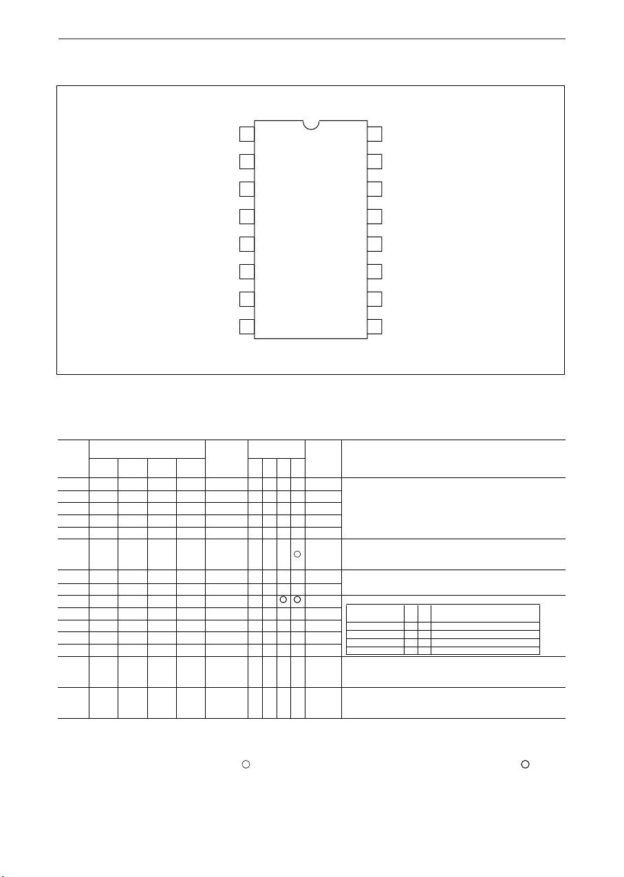
REGISTER TABLE
Address
0
1
2
3
4
5
6
7
8
9
A
B
C
D
E~F
Address input
D
D
(A1)
D
1
2
(A2)
0
0
0
0
1
0
1
0
0
1
1
1
1
1
0
0
0
0
1
0
1
0
0
1
0
(A0)
0
1
0
1
0
1010 H
0
1
0
1
0
1
0
1011
0/1 1 1 1
(A3)
1
CS
2
2
WRITE
3
READ
4
D
0
5
D
1
6
D
2
7
D
3
8
GND
Data input/
S
1
S
10
1
10
H
1
10
W
D
1
D
10
1
10
Y
1
Y
10
output
D
D1D2D
0
*
*
*
*
*
*
*
*
*
*
*
*
*
*
*
****
*
*
*
*
*
*
*
*
*
*
*
*
*
*
*
*
*
*
*
Count value
3
*
*
*
*
*
*
*
*
0 to 9
0 to 5
0 to 9
0 to 5
0 to 9
0~1 or 0~2
0 to 6
0 to 9
0 to 3
0 to 9
0 to 1
0 to 9
0 to 9
Register
Name
D
3
0
0
MI
0
MI
0
0
0
0
1
MO
1
MO
1
1
1
16
V
DD
15
XT
14
XT
13
CS
1
12
TEST
11
STOP
10
BUSY
9
ADDRESS WRITE
Remarks
D2 = 1 specifies PM, D2 = 0 specifies AM, D3 = 1 specifies 24-hour timer, and
D3 = 0 specifies 12-hour timer.
When D3 = 1 is written, the D2 bit is reset inside the IC.
The D2 and D3 bits in D10 are used to select a leap year.
Calendar
Gregorian calendar
A selector to reset 5 poststages in the 1/2
circuit. They are reset when this code is latched with ADDRESS LATCH and
the WRITE input goes to 1.
A selector to obtain reference signal output. Reference signals are output to
D0 – D3 when this code is latched with ADDRESS LATCH and READ input
goes to 1.
Remainder obtained by dividing the
D
D
2
3
0
1
0
1
year number by 4
0
0
1
1
15
0
3
2
1
frequency divider and the BUSY
Note:
8
(1)
There are no bits in blank fields for data input/output. 0 signals are output by reading and data is
not stored by writing because there are no bits.
The bit with marked * is used to select the 12/24-hour timer and the bits marked * are
(2)
used to select a leap year. These three bits can be read or written.
When signals are input to bus lines D0 – D3 and ADDRESS WRITE goes to 1 for address input,
(3)
ADDRESS information is latched with ADDRESS LATCH.
¡ Semiconductor MSM58321
ELECTRICAL CHARACTERISTICS
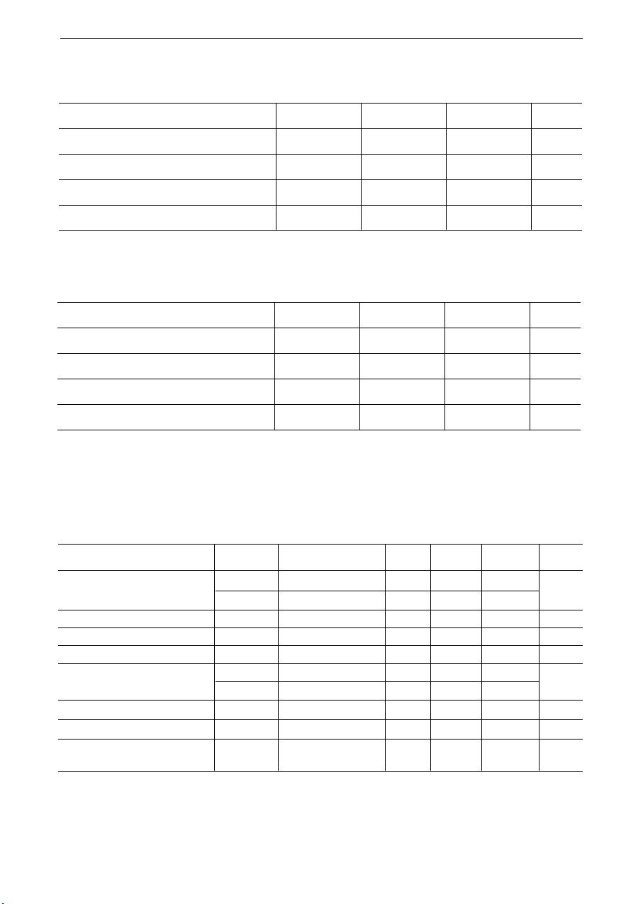
Absolute Maximum Ratings
Rating Symbol Condition Value Unit
Power voltage V
Input voltage V
Output voltage V
Storage temperature T
DD
I
O
stg
Ta = 25°C –0.3 to 6.5 V
Ta = 25°C –0.3 to VDD+0.3 V
Ta = 25°C –0.3 to VDD+0.3 V
– –55 to +150 °C
Operating Conditions
Rating Symbol Condition Value Unit
Power voltage VDD – 4.5 to 6 V
Date hold voltage VDH – 2.2 to 6 V
Crystal frequency ƒ(XT) – 32.768 kHz
Operating temperature TOP – –30 to +85 °C
Note:
The data hold voltage guarantees the clock operations, though it does not guarantee operations outside
the IC and data input/output.
DC Characteristics
(V
= 5V ±5%, Ta = –30 ~ +85°C)
DD
Rating Symbol Condition Max. Unit
H input voltage
L input voltage
L output voltage
L output current
H input current
L input current
Input capacity
Current consumption
Note:
1.
CS
2
CS
2.
1
CS1, CS2, WRITE, READ, ADDRESS WRITE, STOP, TEST
3.
~ D
D
4.
0
V
IH1
V
IH2
V
IL
V
OL
I
OL
I
IH1
I
IH2
I
IL
C
I
I
DD
– Note 1
– Note 2
–
O
= 1.6 mA
I
O
= 0.4 V
V
I
= VDD Note3
V
V
I
= VDD Note4
I
= 0V
V
ƒ = 1 MHz
ƒ = 32.768 kHz
DD
= 5V/VDD = 3V
V
, WRITE, READ, ADDRESS WRITE, STOP, TEST, D0 ~ D
3
V
3
Min.
3.6
–0.5
DD
–
–
1.6
10
–
–
–
–
Typ.
–
–
–
–
–
30
–
–
5
100/15
–
–
0.8
0.4
–
mA
80
1
–1
–
500/30 µA
V
V
V
µA
µA
pF
9
Switching Characteristics
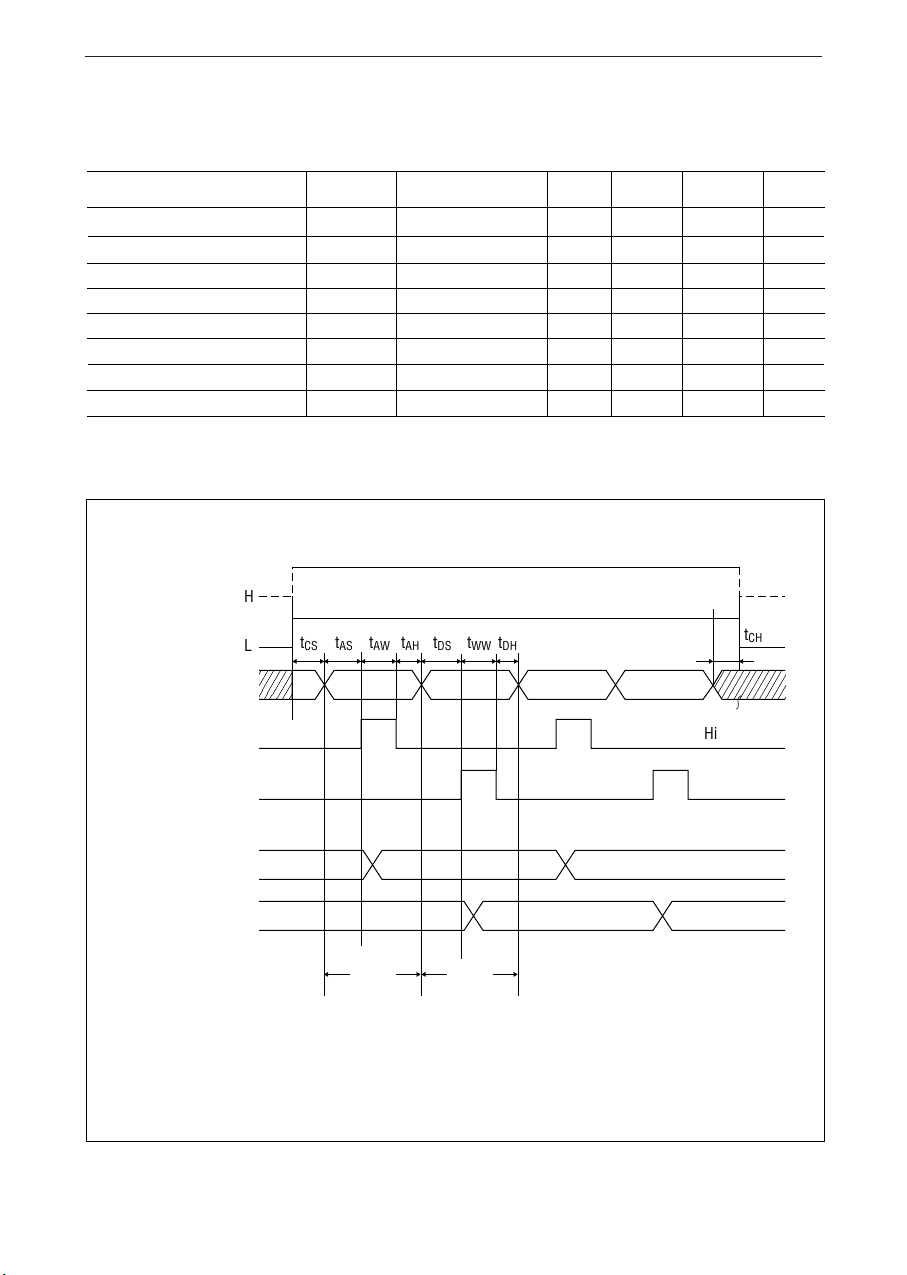
(1) WRITE mode
¡ SemiconductorMSM58321
= 5V ±5%, Ta = 25°C)
(V
DD
Rating Symbol Condition Max. Unit
CS setup time
CS hold time
Address setup time
Address write pulse width
Address hold time
Data setup time
Write pulse width
Data hold time
CS1
CS2
D0 ~ D3
(ADDRESS/DATA)
ADDRESS WRITE
t
CS
t
CH
t
AS
t
AW
t
AH
t
DS
t
WW
t
DH
H
tCStAStAWtAHtDStWWt
L
Min.
–
–
–
–
–
0.5
0.1
–
–
–
DH
Typ.
0
0
0
–
–
–
–
–
0
2
0
–
–
–
–
–
–
–
–
–
–
–
µs
µs
µs
µs
µs
µs
µs
µs
t
CH
High Impedance
WRITE
IC internal
ADDRESS
IC internal DATA
ADDRESS
DATA
Write Cycle
Note: ADDRESS WRITE and WRITE inputs are activated by the level, not by the edge.
10
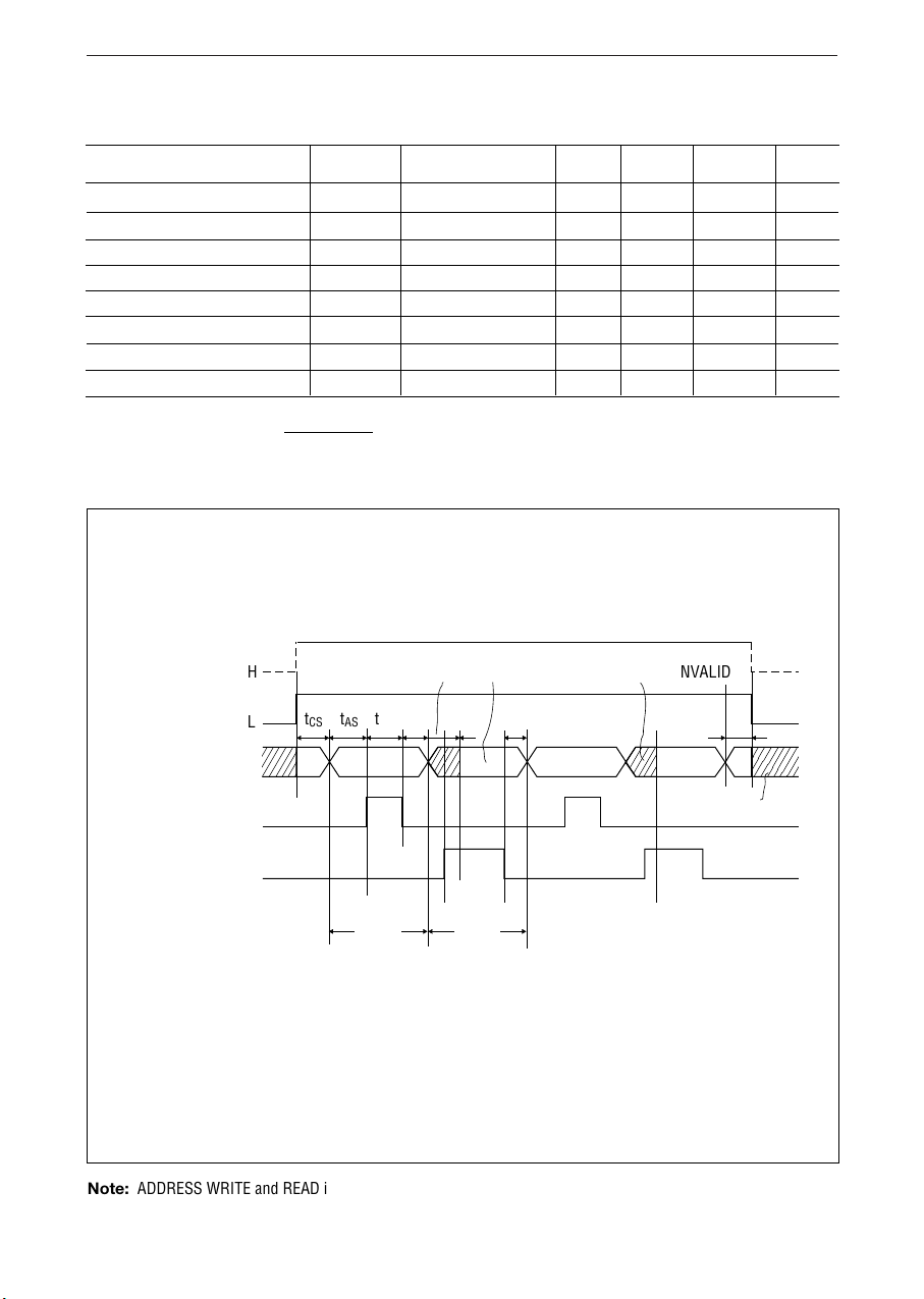
¡ Semiconductor MSM58321
(2) READ mode
= 5V ±5%, Ta = 25°C)
(V
DD
Rating Symbol Condition Max. Unit
CS setup time
CS hold time
Address setup time
Address write pulse width
Address hold time
Read access time
Read delay time
Read inhibit time
Note 1. t
= 1 µs + CR ln ( )
RA
CS1
CS2
D0 ~ D3
(ADDRESS/DATA)
V
– VIH min
DD
H
tCStAStAWtRHt
L
0
0
0
–
–
0
Typ.
–
–
–
–
–
–
see Note 1
–
–
DATA INVALID
–
–
–
–
–
µs
µs
µs
µs
µs
µs
1
–
µs
µs
t
CH
Min.
t
RI
RA
–
–
–
–
–
–
–
–
DATA VALID
t
DD
0.5
0.1
t
CS
t
CH
t
AS
t
AW
t
AH
t
RA
t
DD
t
RI
V
DD
ADDRESS WRITE
READ
ADDRESS
DATA
Read Cycle
Note: ADDRESS WRITE and READ inputs are activated by the level, not by the edge.
High Impedance
11
 Loading...