

Semiconductor
MSM514265E
262,144-Word x 16-Bit DYNAMIC RAM : FAST PAGE MODE TYPE WITH EDO
DESCRIPTION
The MSM514265E is a 262,144-word × 16-bit dynamic RAM fabricated in Oki’s silicon-gate CMOS technology.
The MSM514265E achieves high integration, high-speed operation, and low-power consumption because Oki
manufactures the device in a quadruple-layer polysilicon/double-layer metal CMOS process. The MSM514265E
is available in a 40-pin plastic SOJ or 44/40-pin plastic TSOP.
FEATURES
• 262,144-word × 16-bit configuration
• Single 5V power supply, ±10% tolerance
• Input : TTL compatible, low input capacitance
• Output : TTL compatible, 3-state
• Refresh : 512 cycles/8ms
• Fast page mode with EDO, read modify write capability
• CAS before RAS refresh, hidden refresh, RAS-only refresh capability
• Package options:
40-pin 400mil plastic SOJ (SOJ40-P-400-1.27) (Product : MSM514265E-xxJS)
44/40-pin 400mil plastic TSOP (TSOPII44/40-P-400-0.80-K) (Product : MSM514265E-xxTS-K)
xx indicates speed rank.
PRODUCT FAMILY
Access Time (Max.) Power Dissipation
Family
t
RAC
t
AA
t
CAC
t
OEA
Cycle Time
(Min.)
Operating (Max.) Standby (Max.)
60ns 30ns 15ns 15ns 104ns 633mW
MSM514265E
70ns 35ns 20ns 20ns 124ns 578mW
5.5mW
This version:Aug.2000
MSM514265E
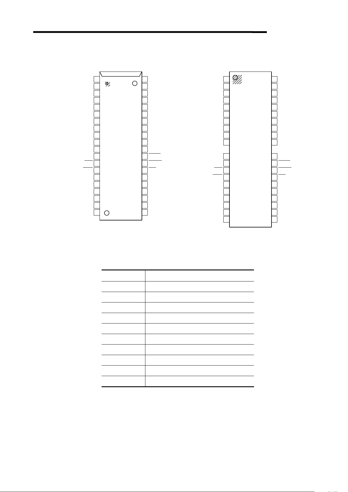
PIN CONFIGRATION (TOP VIEW)
Pin Name Function
A0 − A8
Address Input
RAS
Row Address Strobe
LCAS
Lower Byte Column Address Strobe
UCAS
Upper Byte Column Address Strobe
DQ1–DQ16 Data Input/Data Output
OE
Output Enable
WE
Write Enable
V
CC
Power Supply (5V)
V
SS
Ground (0V)
NC No Connection
Note : The same power supply voltage must be provided to every VCC pin, and the same
GND voltage level must be provided to every VSS pin.
40-Pin Plastic SOJ
44/40-Pin Plastic TSOP
(K Type)
1
2
3
4
5
6
7
8
9
10
11
12
13
14
15
16
17
18
19
20 21
40
39
38
37
36
35
34
33
32
31
30
29
28
27
26
25
24
23
22
DQ1
DQ2
DQ3
DQ4
V
CC
V
CC
V
CC
V
SS
V
SS
V
SS
DQ16
DQ15
DQ14
DQ13
DQ12
DQ11
DQ10
DQ9
A8
A7
A6
A0
A1
A2
A3
DQ5
DQ6
DQ7
DQ8
NC
NC
WE
RAS
NC
NC
A5
A4
LCAS
UCAS
OE
44
43
42
41
40
36
35
39
38
32
31
30
V
SS
V
SS
V
SS
DQ16
DQ15
DQ14
DQ13
DQ12
DQ11
DQ10
DQ9
A8
A7
A6
A5
A4
LCAS
UCAS
OE29
28
27
26
NC
1
2
3
4
5
6
7
8
9
10
DQ1
DQ2
DQ3
DQ4
V
CC
V
CC
DQ5
DQ6
DQ7
DQ8
16
17
18
19
20
21
22 23
24
25
V
CC
A0
A1
A2
A3
NC
WE
RAS
NC
15
NC1413
37
MSM514265E
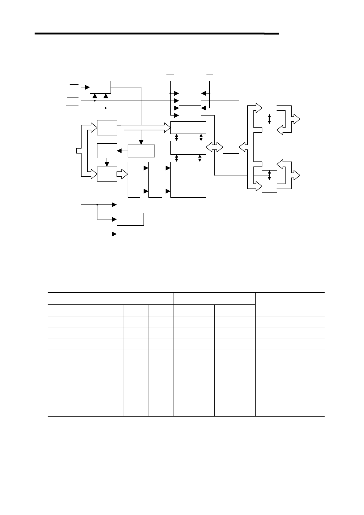
BLOCK DIAGRAM
FUNCTION TABLE
Input Pin DQ Pin
RAS LCAS UCAS WE OE
DQ1-DQ8 DQ9-DQ16
Function Mode
H * * * * High-Z High-Z Standby
L H H * * High-Z High-Z Refresh
L L H H L D
OUT
High-Z Lower Byte Read
L H L H L High-Z D
OUT
Upper Byte Read
L L L H L D
OUT
D
OUT
Word Read
L L H L H D
IN
Don’t Care Lower Byte Write
L H L L H Don’t Care D
IN
Upper Byte Write
L L L L H D
IN
D
IN
Word Write
L L L H H High-Z High-Z
* : “H” or “L”
A0〜A8
8888888168
16
999
9
Timing
Generator
Column
Address
Buffers
I/O
Controller
Internal
Address
Counter
Row
Address
Buffers
Refresh
Control Clock
I/O
Controller
Column Decoders
Sense Amplifiers
Memory
Cells
Word
Drivers
Row
Deco-
ders
I/O
Selector
Input
Buffers
Input
Buffers
Output
Buffers
Output
Buffers
DQ1〜DQ8
DQ9〜DQ16
OEWERAS
LCAS
UCAS
VCCV
SS
On Chip
VBB Generator
MSM514265E
ELECTRICAL CHARACTERISTICS
Absolute Maximum Ratings
Parameter Symbol Rating Unit
Voltage on Any Pin Relative to V
SS
VIN, V
OUT
−0.5 to VCC + 0.5
V
Voltage VCC supply Relative to V
SS
V
CC
−0.5 to 7.0
V
Short Circuit Output Current
I
OS
50 mA
Power Dissipation
P
D*
1 W
Operating Temperature
T
opr
0 to 70 °C
Storage Temperature
T
stg
−55 to 150
°C
*: Ta = 25°C
Recommended Operating Conditions
(Ta = 0°C to 70°C)
Parameter Symbol Min. Typ. Max. Unit
V
CC
4.5 5.0 5.5 V
Power Supply Voltage
V
SS
0 0 0 V
Input High Voltage
V
IH
2.4
V
CC
+ 0.5
*1
V
Input Low Voltage
V
IL
−0.5
*2
0.8 V
Notes: *1. The input voltage is VCC + 2.0V when the pulse width is less than 20ns (the pulse width is with
respect to the point at which VCC is applied).
*2. The input voltage is VSS − 2.0V when the pulse width is less than 20ns (the pulse width respect to
the point at which VSS is applied).
Capacitance
(VCC = 5V ± 10%, Ta = 25°C, f=1MHz)
Parameter Symbol Typ. Max. Unit
Input Capacitance (A0 – A8)
C
IN1
5 pF
Input Capacitance
(RAS, LCAS, UCAS, WE, OE)
C
IN2
7 pF
Output Capacitance (DQ1 - DQ16)
C
I/O
7 pF

MSM514265E
DC Characteristics
(VCC = 5V ± 10%, Ta = 0°C to 70°C)
MSM514265
E-60
MSM514265
E-70
Parameter
Symbol
Condition
Min. Max. Min. Max.
Unit Note
Output High Voltage
V
OH
IOH = −5.0mA
2.4
V
CC
2.4
V
CC
V
Output Low Voltage
V
OL
IOL = 4.2mA
0 0.4 0 0.4 V
Input Leakage Current
I
LI
0V ≤ VI ≤ 6.5V;
All other pins not
under test = 0V
− 10
10
− 10
10
µA
Output Leakage Current
I
LO
DQ disable
0V ≤ VO ≤ VCC
− 10
10
− 10
10
µA
Average Power Supply Current
(Operating)
I
CC1
RAS, CAS cycling,
tRC = Min.
115
105 mA 1,2
RAS, CAS = V
IH
2
2
Power Supply Current
(Standby)
I
CC2
RAS, CAS ≥
VCC − 0.2V
1
1
mA 1
Average Power Supply Current
(RAS-only Refresh)
I
CC3
RAS cycling,
CAS = VIH,
tRC = Min.
115
105 mA 1,2
Power Supply Current
(Standby)
I
CC5
RAS = VIH,
CAS = VIL,
DQ = enable
5
5 mA 1
Average Power Supply Current
(CAS before RAS Refresh)
I
CC6
RAS = cycling,
CAS before RAS
115
105 mA 1,2
Average Power Supply Current
(Fast Page Mode)
I
CC7
RAS = VIL,
CAS cycling,
t
HPC
= Min.
115
105 mA 1,3
Notes: 1. ICC Max. is specified as ICC for output open condition.
2. The address can be changed once or less while RAS = VIL.
3. The address can be changed once or less while CAS = VIH.

MSM514265E
AC Characteristic (1/2)
(VCC = 5V ± 10%, Ta = 0°C to 70°C) Note1,2,3
MSM514265
E-60
MSM514265
E-70
Parameter Symbol
Min. Max. Min. Max.
Unit Note
Random Read or Write Cycle Time
t
RC
104
124
ns
Read Modify Write Cycle Time
t
RWC
135
160
ns
Fast Page Mode Cycle Time
t
HPC
25
30
ns
Fast Page Mode Read Modify Write Cycle Time
t
HPRWC
68
78
ns
Access Time from RAS
t
RAC
60
70 ns 4, 5, 6
Access Time from CAS
t
CAC
15
20 ns 4,5
Access Time from Column Address
t
AA
30
35 ns 4,6
Access Time from CAS Precharge
t
CPA
35
40 ns 4,13
Access Time from OE
t
OEA
15
20 ns 4
Output Low Impedance Time from CAS
t
CLZ
0
0
ns 4
Data Output Hold After CAS Low
t
DOH
5
5
ns
CAS to Data Output Buffer Turn-off Delay Time
t
CEZ
0 15 0 20 ns 7,8
RAS to Data Output Buffer Turn-off Delay Time
t
REZ
0 15 0 20 ns 7,8
OE to Data Output Buffer Turn-off Delay Time
t
OEZ
0 15 0 20 ns 7
WE to Data Output Buffer Turn-off Delay Time
t
WEZ
0 15 0 20 ns 7
Transition Time
t
T
1 50 1 50 ns 3
Refresh Period
t
REF
8
8 ms
RAS Precharge Time
t
RP
40
50
ns
RAS Pulse Width
t
RAS
60 10,000 70 10,000 ns
RAS Pulse Width (Fast Page Mode with EDO)
t
RASP
60 100,000 70 100,000 ns
RAS Hold Time
t
RSH
10
13
ns
RAS Hold Time referenced to OE
t
ROH
10
13
ns
CAS Precharge Time
(Fast Page Mode with EDO)
t
CP
10
10
ns 15
CAS Pulse Width
t
CAS
10 10,000 10 10,000 ns
CAS Hold Time
t
CSH
40
45
ns
CAS to RAS Precharge Time
t
CRP
5
5
ns 13
RAS Hold Time from CAS Precharge
t
RHCP
35
40
ns 13
OE Hold Time from CAS (DQ Disable)
t
CHO
5
5
ns
RAS to CAS Delay Time
t
RCD
14 45 14 50 ns 5
RAS to Column Address Delay Time
t
RAD
12 30 12 35 ns 6
Row Address Set-up Time
t
ASR
0
0
ns
Row Address Hold Time
t
RAH
10
10
ns

MSM514265E
AC Characteristic (2/2)
(VCC = 5V ± 10%, Ta = 0°C to 70°C) Note1,2,3
MSM514265
E-60
MSM514265
E-70
Parameter Symbol
Min. Max. Min. Max.
Unit Note
Column Address Set-up Time
t
ASC
0
0
ns 12
Column Address Hold Time
t
CAH
10
13
ns 12
Column Address to RAS Lead Time
t
RAL
30
35
ns
Read Command Set-up Time
t
RCS
0
0
ns 12
Read Command Hold Time
t
RCH
0
0
ns 9,12
Read Command Hold Time referenced to RAS
t
RRH
0
0
ns 9
Write Command Set-up Time
t
WCS
0
0
ns 10,12
Write Command Hold Time
t
WCH
10
13
ns 12
Write Command Pulse Width
t
WP
10
10
ns
WE Pulse Width (DQ Disable)
t
WPE
7
7
ns
OE Command Hold Time
t
OEH
10
13
ns
OE Precharge Time
t
OEP
10
10
ns
OE Command Hold Time
t
OCH
10
10
ns
Write Command to RAS Lead Time
t
RWL
10
13
ns
Write Command to CAS Lead Time
t
CWL
10
13
ns 14
Data-in Set-up Time
t
DS
0
0
ns 11,12
Data-in Hold Time
t
DH
10
13
ns 11,12
OE to Data-in Delay Time
t
OED
15
20
ns
CAS to WE Delay Time
t
CWD
35
45
ns 10
Column Address to WE Delay Time
t
AWD
50
60
ns 10
RAS to WE Delay Time
t
RWD
80
95
ns 10
CAS Precharge WE Delay Time
t
CPWD
55
65
ns 10
CAS Active Delay Time from RAS Precharge
t
RPC
5
5
ns 12
RAS to CAS Set-up Time (CAS before RAS)
t
CSR
5
5
ns 12
RAS to CAS Hold Time (CAS before RAS)
t
CHR
10
10
ns 13

MSM514265E
Notes: 1. A start-up delay of 200µs is required after power-up, followed by a minimum of eight initialization
cycles (RAS-only refresh or CAS before RAS refresh) before proper device operation is achieved.
2. The AC characteristics assume tT = 2ns.
3. VIH (Min.) and VIL (Max.) are reference levels for measuring input timing signals. Transition times
(tT) are measured between VIH and VIL.
4. This parameter is measured with a load circuit equivalent to 1 TTL load and 50pF.
The output timing reference levels are VOH = 2.0V (IOH = −2mA) and VOL = 0.8V (IOH = 2mA).
5. Operation within the t
RCD
(Max.) limit ensures that t
RAC
(Max.) can be met.
t
RCD
(Max.) is specified as a reference point only. If t
RCD
is greater than the specified t
RCD
(Max.)
limit, then the access time is controlled by t
CAC
.
6. Operation within the t
RAD
(Max.) limit ensures that t
RAC
(Max.) can be met.
t
RAD
(Max.) is specified as a reference point only. If t
RAD
is greater than the specified t
RAD
(Max.)
limit, then the access time is controlled by tAA.
7. t
CEZ
(Max.), t
REZ
(Max.), t
WEZ
(Max.), and t
OEZ
(Max.) define the time at which the output
achieved the open circuit condition and are not referenced to output voltage levels.
8. t
CEZ
, and t
REZ
must be satisfied for open circuit condition.
9. t
RCH
or t
RRH
must be satisfied for a read cycle.
10. t
WCS
, t
CWD
, t
RWD
, t
AWD
and t
CPWD
are not restrictive operating parameters. They are included in
the data sheet as electrical characteristics only. If t
WCS
≥ t
WCS
(Min.), then the cycle is an early
write cycle and the data out will remain open circuit (high impedance) throughout the entire cycle.
If t
CWD
≥ t
CWD
(Min.), t
RWD
≥ t
RWD
(Min.), t
AWD
≥ t
AWD
(Min.) and t
CPWD
≥ t
CPWD
(Min.), then
the cycle is a read modify write cycle and data out will contain data read from the selected cell; if
neither of the above sets of conditions is satisfied, then the condition of the data out (at access time)
is indeterminate.
11. These parameters are referenced to the UCAS and LCAS, leading edges in an early write cycle,
and to the WE leading edge in an OE control write cycle, or a read modify write cycle.
12. These parameters are determined by the falling edge of either UCAS or LCAS, whichever is
earlier.
13. These parameters are determined by the rising edge of either UCAS or LCAS, whichever is later.
14. t
CWL
should be satisfied by both UCAS and LCAS.
15. tCP is determined by the time both UCAS and LCAS are high.

MSM514265E
9/14
Timing Chart
• Read Cycle
• Write Cycle (Early Write)
t
RAStCEZtCLZ
t
CAC
t
AOEtASCtRRHtRAHtASR
t
RADtRAL
t
CRPtCAHtCRPtRCDtRCtRPtCSHtRSHtCAS
t
RACtAA
t
RCStROHtRCHtREZ
t
OEZ
Row
Column
Valid Data-out
Open
RAS
VIHVILCAS
VIHVILAddress
VIHVILWE
VIHVILOE
V
IH
VILDQ
VOHV
OL
“H” or “L”
t
WCS
t
WCH
t
CWL
t
ASRtRAHtASC
t
CRP
t
RP
tRCt
RAStDH
t
RWLtCSH
t
CRP
t
RCDtRSHtCAStCAH
t
RADtRAL
t
DS
t
WP
Valid Data-in
Row Column
RAS
V
IH
V
IL
CAS
VIHVILAddress
V
IH
VILWE
V
IH
VILOE
VIHVILDQ
V
IH
V
IL
“H” or “L”
Open

MSM514265E
10/14
• Read Modify Write Cycle
t
DH
tDSt
OEZtCLZtOEDtAAtOEH
t
RWDtCWD
t
CWLtRWLtCAHtASCtASR
t
RAH
t
RAD
t
CRP
t
RCDtRSHtCAStCRP
t
CAC
t
CSHtRAC
t
OEA
t
RCStAWD
tWPt
RWCtRAS
t
RP
Valid
Data-out
Row Column
RAS
V
IH
VILCAS
VIHVILAddress
V
IH
VILWE
V
IH
VILOE
VIHVILDQ
V
I/OH
V
I/OL
“H” or “L”
Valid
Data-in

MSM514265E
11/14
• Fast Page Mode Read Cycle (Part-1)
• Fast Page Mode Read Cycle (Part-2)
t
AA
t
OEPtCHOtCACtOEPtCACtCPA
tAAt
OEAtAAtRAC
t
RRHtOCH
t
CAHtASC
t
RAHtRADtRCS
t
ASR
t
ASCtCAH
tCPt
CAS
t
HPCtRASP
t
CAStCPtCSH
t
CRP
t
CLZ
t
CAHtOEAtOEAtOEZ
t
CAC
t
ASCtRPtRHCP
t
CAStDOHtOEZtREZ
t
RCD
Valid
Data-out
Valid *
Data-out
Valid *
Data-out
Valid
Data-out
RAS
V
IH
VILCAS
V
IH
VILAddress
VIHVILWE
V
IH
VILOE
V
IH
VILDQ
VOHV
OL
Row Column Column Column
“H” or “L”* : Same Dada,
t
CEZtCACtDOHtCACtCPAtRCH
t
RCS
t
OEAtRACtAA
t
RCS
t
CRPtASR
t
CAH
t
ASCtRAH
t
RAD
t
ASCtCPtASCtCAHtCAStCPtCAStRHCPtCSHtHPCtCLZtCAHtAAtWEZtCACtCAStRP
t
RASP
t
WPEtRCD
Valid
Data-out
Valid
Data-out
Valid
Data-out
t
AA
RAS
VIHVILCAS
V
IH
VILAddress
V
IH
VILWE
VIHVILOE
V
IH
VILDQ
V
OH
V
OL
Row Column Column Column
“H” or “L”

MSM514265E
12/14
• Fast Page Mode Write Cycle (Early Write)
• Fast Page Mode Read Modify Write Cycle
tDHtDStDHtDStDHt
DS
t
WCHtWCStWCStWCHtWCHtWCS
t
ASC
t
CAH
t
ASC
t
CAHtRAD
t
ASRtASCtRAHtRCDtCRPtCAStCAStRSHtCPtCAS
t
RP
t
HPCtCSH
t
CAH
tCPt
HPCtRASP
Valid
Data-in
Valid
Data-in
Valid
Data-in
“H” or “L”
RAS
VIHVILCAS
V
IH
VILAddress
V
IH
VILWE
VIHVILOE
V
IH
VILDQ
V
IH
V
IL
Row Column Column Column
t
OEDtDHtOEZtOEHtCACtOEDtDHtOEZtOEHtAWDtAWDtWP
t
DS
t
AA
tDSt
CWDtRCStRAH
t
CAHtASR
t
RADtHPRWC
t
CPAtCWLtCAHtASCtCP
t
RWLtRWD
t
CWDtRCD
t
CRPtRASP
t
OEA
t
RCStASC
t
WP
t
CPWD
t
RACtCACtCLZtCLZ
Column
RAS
V
IH
VILCAS
V
IH
VILAddress
V
IH
VILWE
VIHVILOE
V
IH
VILDQ
V
I/OHVI/OL
Row Column
Valid *
Data-in
Valid *
Data-out
Valid *
Data-in
Valid *
Data-out
“H” or “L”

MSM514265E
13/14
• RAS-Only Refresh Cycle
• CAS before RAS Refresh Cycle
t
CEZtRPCtRPtRCtRAStCHRtCSRtRPtCPtRPC
RAS
VIHVILCAS
V
IH
VILV
OH
V
OL
DQ
Open
Note: WE, OE, Address = “H” or “L”
t
ASRtRAHtCRPtRPCtRPtRAStRC
t
CEZ
RAS
VIHVILCAS
V
IH
VILV
IH
V
IL
Address
VOHV
OL
DQ
“H” or “L”
Note: WE, OE = “H” or “L”
Row
Open

MSM514265E
14/14
• Hidden Refresh Read Cycle
• Hidden Refresh Write Cycle
tDHtDSt
WCH
t
WCStRWLtRAL
t
RADtCAH
t
RAH
t
ASRtASCtRCD
t
CRP
t
RSHtRPtCHR
tRPt
RAStRCtRCtRAStWP
RAS
V
IH
VILCAS
VIHVILAddress
V
IH
VILWE
V
IH
VILOE
VIHVILDQ
V
IH
V
IL
Row Column
Valid Data-in
“H” or “L”
t
RAC
t
CLZtOEZtROHtOEA
t
CACtRRH
tAAt
RAL
t
RCS
t
CAHtRAHtASRtASC
t
RAD
tRPt
RAStRCtRPtCHRtRAStRSHtRCDtCRPtRCtWRH
t
WRP
Column
RAS
VIHVILCAS
V
IH
VILAddress
V
IH
VILWE
VIHV
IL
OE
V
IH
VILDQ
V
OH
V
OL
Open
Row
Valid Data-out
“H” or “L”

NOTICE
1. The information contained herein can change without notice owing to product and/or
technical improvements. Before using the product, please make sure that the information
being referred to is up-to-date.
2. The outline of action and examples for application circuits described herein have been
chosen as an explanation for the standard action and performance of the product. When
planning to use the product, please ensure that the external conditions are reflected in the
actual circuit and assembly designs.
3. When designing your product, please use our product below the specified maximum
ratings and within the specified operating ranges including, but not limited to, operating
voltage, power dissipation, and operating temperature.
4.
OKI assumes no responsibility or liability whatsoever for any failure or unusual or
unexpected operation resulting from misuse, neglect, improper installation, repair, alteration
or accident, improper handling, or unusual physical or electrical stress including, but not
limited to, exposure to parameters beyond the specified maximum ratings or operation
outside the specified operating range.
5.
Neither indemnity against nor license of a third party's industrial and intellectual property
right, etc. is granted by us in connection with the use of the product and/or information
and drawings contained herein. No responsibility is assumed by us for any infringement
of a third party's right which may result from the use thereof.
6.
The products listed in this document are intended for use in general electronics equipment
for commercial applications (e.g., office automation, communication equipment,
measurement equipment, consumer electronics, etc.). These products are not authorized
for use in any system or application that requires special or enhanced quality and reliability
characteristics nor in any system or application where the failure of such system or
application may result in the loss or damage of property, or death or injury to humans.
Such applications include, but are not limited to:traffic control, automotive, safety, aerospace,
nuclear power control, and medical, including lift support and maintenance.
7. Certain products in this document may need government approval before they can be
exported to particular countries. The purchaser assumes the responsibility of determining
the legality of export of these products and will take appropriate and necessary steps at their
own expense for these.
8. No part of the contents contained herein may be reprinted or reproduced without our prior
permission.
Copyright 1997 OKI ELECTRIC INDUSTRY CO.,LTD.
 Loading...