E2A0032-16-X0
¡ Semiconductor MSA4709A
¡ Semiconductor
This version: Jan. 1998
Previous version: Nov. 1996
MSA4709A
Subscriber Line Interface Circuit
GENERAL DESCRIPTION
The MSA4709A is designed to provide BSH functions and to meet PABX transmission performance
requirements.
This device provides two-wire to four-wire conversion function (Hybrid).
FEATURES
• B (Battery feed), S (Supervision), and H (Hybrid) functions integrated on chip.
• Design to meet Central Office and PABX quality transmission requirements.
• All transmission performance parameters can be externally programmable.
• Free from parasitic SCR's using dielectric isolation technology.
• Size and weight reduction over conventional approaches.
• Supply voltage selectable (V
• 1 channel built-in relay driver.
• Package:
30-pin plastic Shrink DIP (SDIP30-P-400-1.78) (Product name: MSA4709ASS)
= –24 V/–48 V).
BB
1/11

¡ Semiconductor MSA4709A
2/11
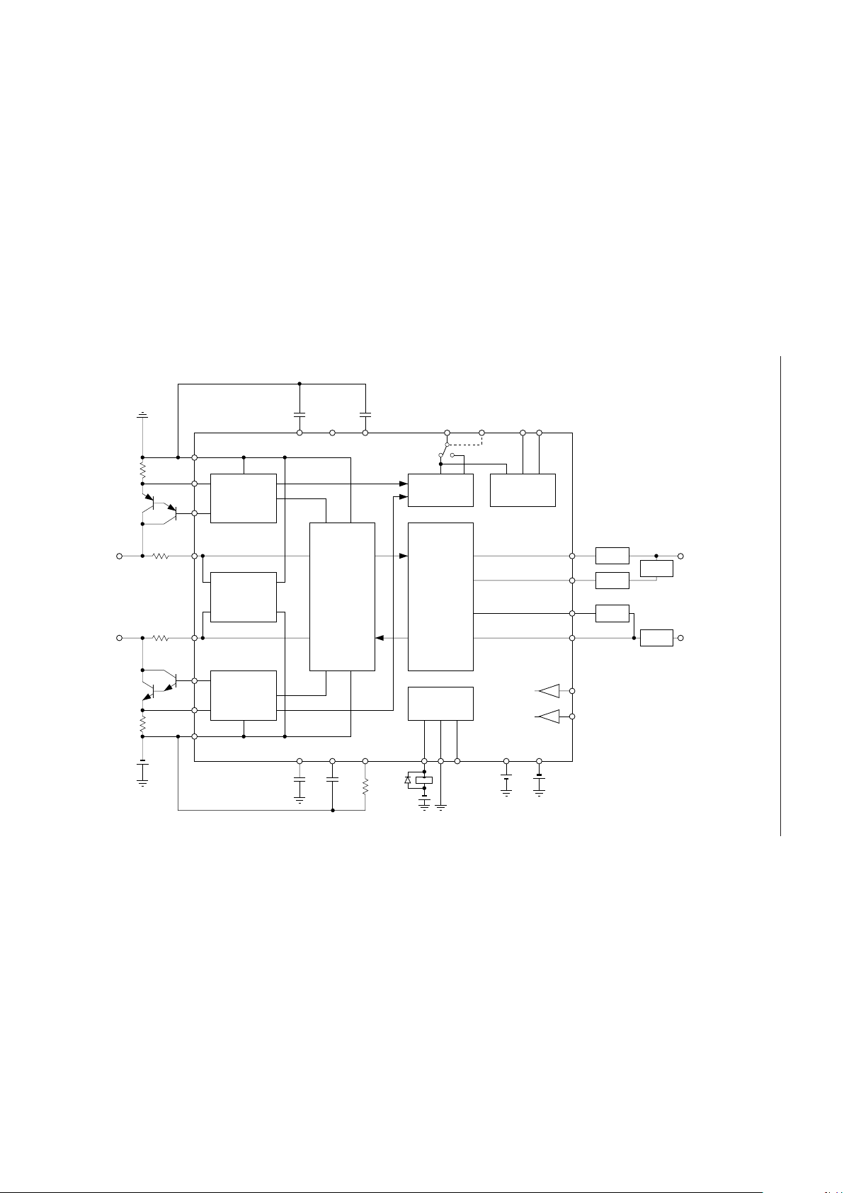
BLOCK DIAGRAM
Ring Current
DET
Ring Current
Drive Amp.
Over Voltage
Protection
TIP Current
DET
TIP Current
Drive Amp.
Interface
Circuit
HYB
Loop & Fault
DET
RING TRIP
Relay Driver
TIP
RING
Z
t
Z
FR
Z
R
Z
b
4WR
ZR
BN
ZX
4WS
4WR
Z
X
VBS
BF
SCN SEL RG RB
V
EE
V
CC
RI
RSI
RSO
V
BB
or
V
EE
RY
CDC
CN
V
BB
NE
NB
A
B
PB
PE
G
CB IL
CDP

¡ Semiconductor MSA4709A
PIN CONFIGURATION (TOP VIEW)
30
29
28
27
26
25
24
NC
B
PE
PB
G
CB
ZX
V
BB
NE
NB
RSO
CN
RY
1
2
A
3
4
5
6
7
Note: NC: No connect pin
CDC
8
RSI
9
RB
10
RG
11
V
12
EE
13
4WR
14
BN
15 16
ZR
30-Pin Plastic Shrink DIP
23
22
21
20
19
18
17
V
CC
RI
BF
VBS
IL
CDP
SEL
SCN
3/11

¡ Semiconductor MSA4709A
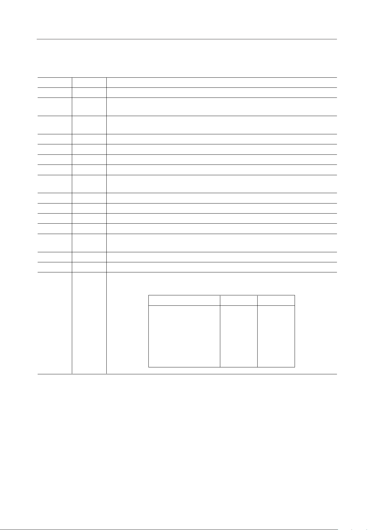
PIN DESCRIPTION
Pin No. Name Description
1VBBBattery supply, –48 V or –24 V input.
2A
3NE
4 NB The base drive output for the NPN Darlington transistor.
5 RSO Relay driver current sink terminal.
6 CN Battery noise rejection capacitor input. This capacitor value is 1 mF (60V).
7 RY AC performance adjusting resistor RY input.
8 CDC
9 RSI Relay driver current source terminal.
10 RB Ring-Trip filtering capacitor input (RING).
11 RG Ring-Trip filtering capacitor input (TIP).
12 V
13 4WR
14 BN Balancing network drive output.
15 ZR Receive gain adjust and frequency compensation input.
EE
The Ring voltage sensing input. This input is high impedance (apr. 37 kW), and is
connected to the built-in over voltage protection circuit.
The Ring current sensing input is connected to the emitter of NPN Darlington transistor
and the power resistor REA.
AC high impedance providing capacitor Cdc input and constant current feed at the short
line adjusting zener diode input. This capacitor value is 1 mF (15V).
–5 V input.
Receive input and is connected to the negative input of the built-in buffer operational
amplifier.
Output of both the fault current detector and loop current detector. This output is opencollector with a built-in pull-up resistor. (apr. 10 kW).
16 SCN
Condition SEL = "H" SEL = "L"
• ON-Hook H H
• OFF-Hook L H
• Dial pulse: break H H
• Dial pulse: make L H
• RING TRIP L H
• Ground/Battery fault L L
4/11
 Loading...