OKI MSA180RS, MSA180MS-K Datasheet
E2D0049-39-21
¡ Semiconductor
This version: Feb. 1999
Previous version: May. 1997
MSA180¡ Semiconductor
MSA180
Piezo Speaker Amplifier
GENERAL DESCRIPTION
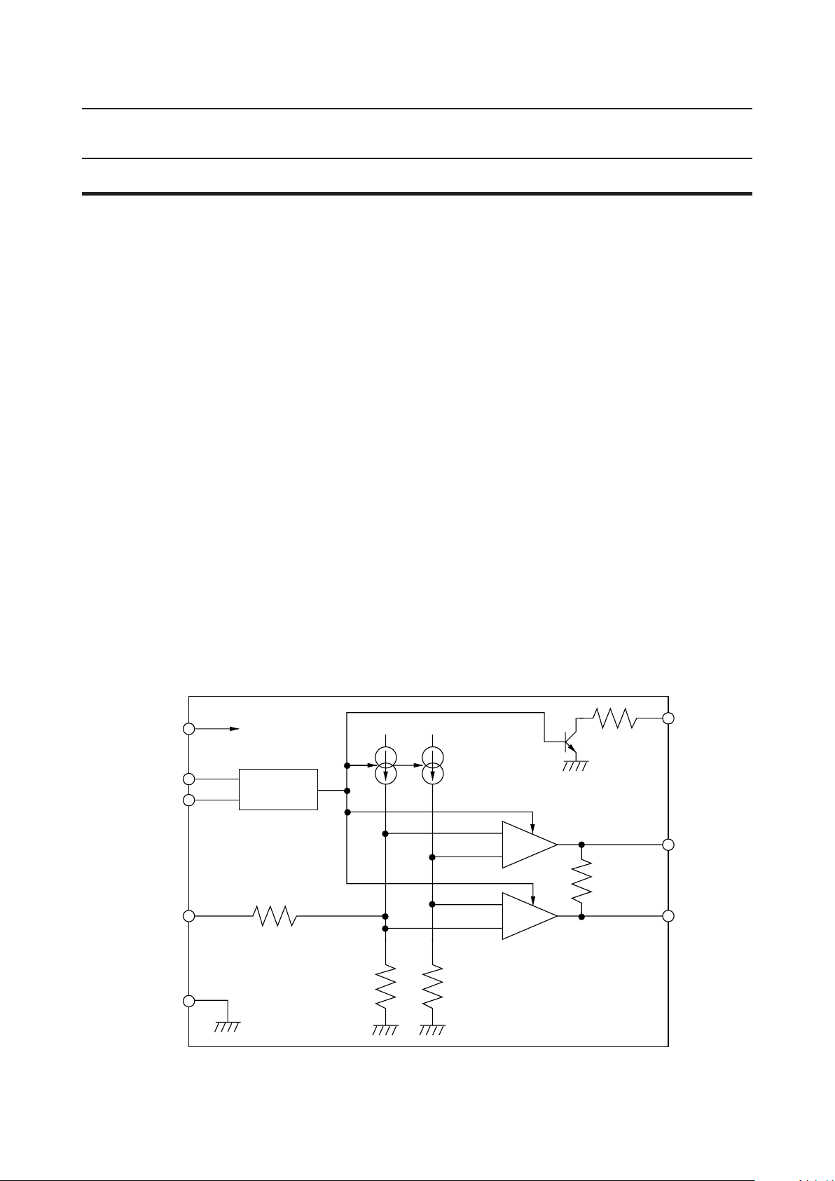
The MSA180 is a piezo speaker driver for OKI's speech synthesizers. Its voltage gain can be adjusted
by a factor of up to 10. The differential output provides an amplitude of twice the voltage supply.
A separate output connects to the base of an external transistor for controlling system voltage.
A standby function eliminates power loss when no input signal is present.
FEATURES
• Power supply voltage : 2.0 V to 6.0 V (single supply voltage)
• Low current consumption : 4.2 mA typ (VCC=3 V, no load)
• Standby current : <1 mA
• Differential output : Twice the supply voltage (maximum output
amplitube)
• Package options :
8-pin plastic DIP (DIP8-P-300-2.54) (Product name: MSA180RS)
8-pin plastic SOP (SOP8-P-250-1.27-K) (Product name: MSA180MS-K)
Chip
BLOCK DIAGRAM
V
CC
MODE1
MODE2
A
IN
GND
Logic
18 kW
CC
V
CC
2.2 kW
+
AV=20
–
1.3 kW
+
=20
A
V
–
6.6 kW6.6 kW
V
BASE
SP
SP
1/16

PIN CONFIGURATION (TOP VIEW)
MSA180¡ Semiconductor
MODE2
A
GND
SP
1
2
IN
3
4
8
7
6
5
MODE1
BASE
V
CC
SP
8-Pin Plastic DIP or 8-Pin Plastic SOP
PIN DESCRIPTIONS
Pin Type Description
6V
3 GND — Ground pin.
2A
8 MODE1 I
1 MODE2 I
7 BASE O
4 SP O
5SPO
Symbol
CC
IN
— Power supply pin.
I Voice signal input pin.
This pin switches the device between operation and standby modes.
The IC is in operation mode if V
standby mode if V
IL
MODE2 must be connected to V
This pin switches the device between operation and standby modes.
The IC is in operation mode if V
standby mode if V
IH
MODE1 must be connected to GND.
This pin is connected to the base of an external transistor. If an
external transistor is not used to control system voltage, this pin must
be left open.
This is a speaker output pin that provides signals with the same phase
as the input.
This is a speaker output pin that provides signals with an inverted
phase to the input.
< 0.3 V on the MODE1 pin. When MODE1 is used,
> VCC–0.3 V on MODE1 pin. When MODE2 is used
> 1.0 V on the MODE1 pin and is in
IH
.
CC
< VCC–1.0 V on MODE1 pin and is in
IL
2/16
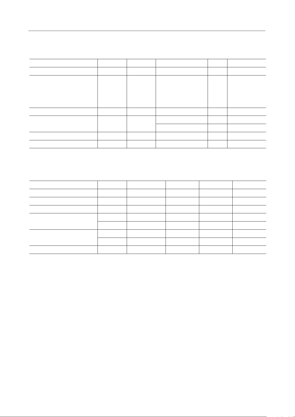
ABSOLUTE MAXIMUM RATINGS
Parameter Symbol Condition Rating Unit Remarks
Power Supply Voltage V
Input Voltage V
Maximum Output Current I
OMAX
Power Dissipation P
Junction Temperature T
Storage Temperature T
CC
IN
D
jMAX
STG
— –0.3 to +6.5 V —
— –0.3 to VCC+0.3 V
VCC=3 V ±80 mA SP, SP
Ta=25°C
— 110 °C Chip
— –55 to +150 °C —
RECOMMENDED OPERATING CONDITIONS
MSA180¡ Semiconductor
(Ta=25°C unless otherwise specified)
A
IN
MODE1
MODE2
BASE
400 mW DIP type
340 mW SOP type
Parameter Symbol Min. Max. UnitCondition
Power Supply Voltage V
Load Impedance Z
Peak Load Current I
V
"H" Input Voltage
V
V
"L" Input Voltage
V
Operating Temperature T
CC
O-P
IH1
IH2
IL1
IL2
op
L
Applied to MODE1 pin
Applied to MODE2 pin
Applied to MODE1 pin
Applied to MODE2 pin
2.0 6.0 V—
200 — W—
— ±30 mA—
1.0 — V
VCC–0.3 — V
— 0.3 V
—V
–1.0 V
CC
–40 +85 °C—
3/16
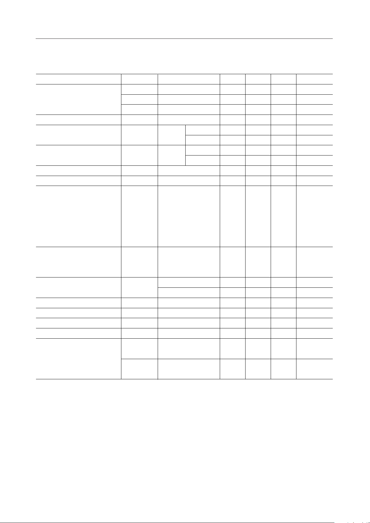
ELECTRICAL CHARACTERISTICS
Parameter Symbol Condition Min. Typ. Max. Unit
A
V1
Voltage Gain
AIN Input Resistance R
Output DC Voltage
Output DC Offset Voltage
*1
*2
SP, SP Output "H" Voltage V
SP, SP Output "L" Voltage V
Operating Current I
Circuit Current in Standby Mode I
AIN Input DC Bias Voltage V
*3
MODE1 "H" Input Current I
MODE2 "H" Input Current I
MODE1 "L" Input Current I
MODE2 "L" Input Current I
Base Output Current
A
A
V
DV
CCS
IH1
IH2
IL1
IL2
I
BO1
I
BO2
V2
V3
IN
O
O
OH
OL
CC
AIN
(Ta=25°C, V
=2 V to 6 V unless otherwise specified)
CC
AINÆSP 4.25 5 5.75 V/V
AINÆSP 4.25 5 5.75 V/V
AINÆ(SP-SP) 8.5 10 11.5 V/V
— 17.2 24.6 32.0 kW
=2 V 0.7 1.0 1.3 V
V
No signal
SP-SP
I
OUT
I
OUT
CC
=6 V 2.5 3.5 4.6 V
V
CC
V
=2 V — — 0.2 V
CC
=6 V — — 0.6 V
V
CC
=–10 mA VCC–0.25 — — V
=10 mA — — 0.25 V
=3 V
V
CC
Z
=•
L
BASE=Open
— 4.2 6.2 mA
MODE1=MODE2=GND
or
MODE1=MODE2=V
CC
AIN=Open
—— 1 µAMODE1=GND
MODE2=V
CC
VCC=2 V 0.18 0.26 0.34 V
=6 V 0.52 0.74 0.96 V
V
CC
MODE1=V
MODE2=V
CC
CC
— — 160 µA
—— 1 µA
MODE1=GND –1 — — µA
MODE2=GND –160 — — µA
VCC=2 V
0.4 — — mA
BASE=V
CC
VCC=6 V
1.6 — — mA
BASE=V
CC
MSA180¡ Semiconductor
*1 Typical value is VO = V
CC
*2 Maximum value is DVO = V
*3 Typical value is V
AIN
= V
CC
¥ 0.625 – 0.25.
¥ 0.1.
CC
¥ 0.12 + 0.02.
4/16
MSA180¡ Semiconductor
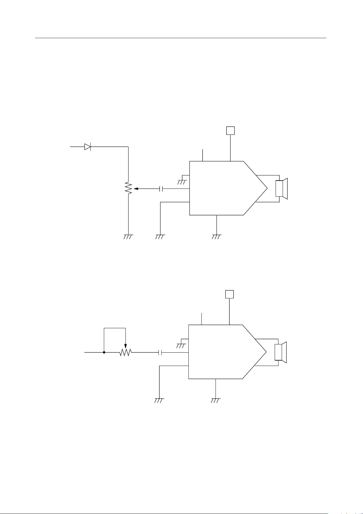
APPLICATION CIRCUITS
How to Adjust Gain
Gain control adjustment of the input signal level is shown below. When using OKI's speech
synthesizer devices, insert a diode in series with the variable resistor to reduce pop noise.
V
DD
Signal
R1
100 kW
C1
0.1 mF
BASE
MODE2
A
IN
MODE1
V
MSA180
CC
PIEZO SPEAKER
SP
SP
GND
The circuit below also implements gain adjustment for a higher impedance signal source.
V
DD
Signal
R1
20 kW
C1
0.1 mF
BASE
MODE2
A
IN
MODE1
V
MSA180
GND
CC
PIEZO SPEAKER
SP
SP
5/16
MSA180¡ Semiconductor
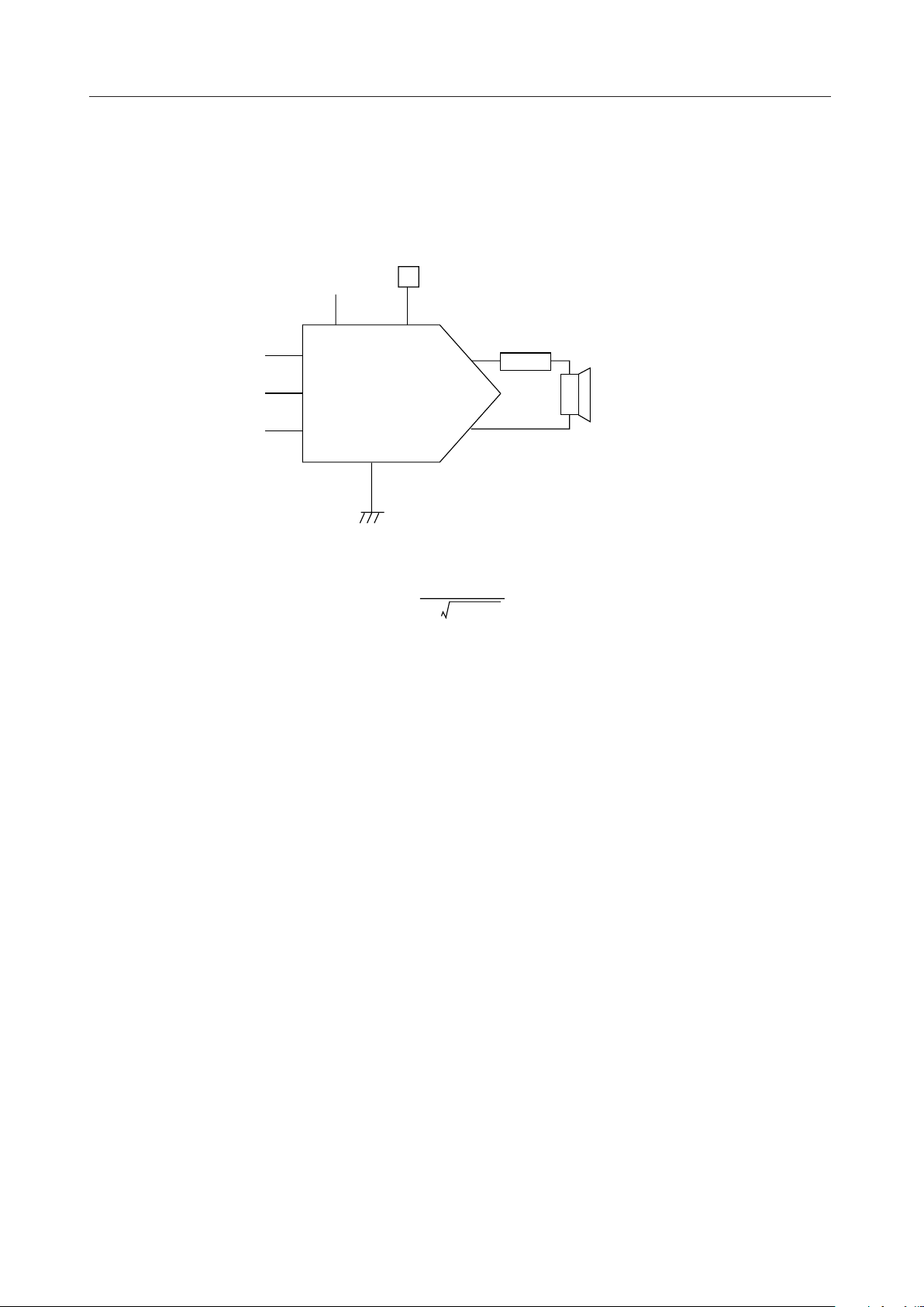
How to Connect the Piezo Speaker
To achieve the full gain level of 10 V, even at a low supply voltage (VCC=3 V), connect a coil in series
with the piezo speaker.
V
DD
BASE
MODE2
A
IN
MODE1
V
MSA180
CC
SP
SP
COIL
PIEZO SPEAKER
GND
The resonance frequency that occurs in the circuit containing the coil and the piezo speaker is :
fQ =
2p C
1
L
¥ L
[Hz]
L
Where CL is the piezo capacitance and LL the coil inductance.
For instance, if the piezo capacitance is 0.1 mF and fQ is in a range of 2 to 3 kHz, then the coil inductance should be 30 mH.
6/16
 Loading...