
PEDS87V1021-01
1
Semiconductor
This version: Sept. 2000
MS87V1021
Recording and Playback IC with Built-in 2-Mbit DRAM
GENERAL DESCRIPTION
The MS87V1021 is a singl e chip recording and pl ayback IC that is con trolled by the microcon troller in s erial mode,
compresses voice with the 4-bit OKI ADPCM algorithm or 4-bit OKI ADPCM2 algorithm with high tone quality,
and has 2-Mbit DRAM in w hich recorded dat a is stored and 512- K bit mask ROM in which fixed messages reside.
The MS87V1021 includes such features as Normal Recording and Playback, Delayed playback, Retroactive
playback, Fast forwarding, and Rewinding.
The internal memory in which voice data is stored allows a recording/playback system to be constructed merely by
externally connecting it to a microphone, a speaker driving amplifier, and a speaker.
FEATURES
• Serial microcontroller interface (clock synchronized)
• Built-in 512-Kbit mask ROM for fixed messages
ROM playback time :
Approx. 15 seconds (Fsam = 8.0 kHz)
Approx. 20 seconds (Fsam = 6.4 kHz)
Approx. 30 seconds (Fsam = 4.0 kHz)
• Voice analyzing and synthesizing system :
4-bit OKI ADPCM or 4-bit OKI ADPCM2 algorithm
8-bit OKI non-linear PCM algorithm (for ROM playback only)
• Sampling frequency (source oscillation frequency: 4.096 MHz) :
4.0 kHz, 5.3 kHz, 6.4 kHz, 8.0 kHz, or 10.6 kHz
• Recording time:
Approx. 60 seconds (Fsam = 8.0 kHz)
Approx. 80 seconds (Fsam = 6.4 kHz)
Approx. 120 seconds (Fsam = 4.0 kHz)
• Built-in 14-bit A-to-D and D-to-A converters
• Built-in LPF: Attenuation rate –40 dB/oct
• Number of phrases
Variable message: 255 phrases
Fixed phrases: 255 phrases
• Source oscillation frequency: 4.096 MHz
• Supply voltage: 2.7 to 3.6 V
• Operating current:
15 mA max. (source oscillation frequency : 4.096 MHz, Supply voltage : 3.6 V)
• Operating temperature: –20 to +70° C
• Package: 32-pin TSOP Type I
1/63

PEDS87V1021-01
1
Semiconductor
MS87V1021
CONTENTS
GENERAL DESCRIPTION.................................................................................................................................1
FEATURES ....................................................................................................................... ...................................1
BLOCK DIAGRAM.............................................................................................................................................4
PIN CONFIGURATION (TOP VIEW)................................................................................................................4
PIN DESCRIPTION.............................................................................................................................................5
APPLICATION CIRCUIT EXAMPLE................................................................................................................6
ABSOLUTE MAXIMUM RATINGS..................................................................................................................7
RECOMMENDED OPERATING CONDITIONS...............................................................................................7
ELECTRICAL CHARACTERISTICS.................................................................................................................7
DC Characteristics. .............................................................................................................................................7
AC Characteristics ..............................................................................................................................................8
1. Microcontroller interface mode....................................................................................................................8
2. BUSY time when a command is executed..................................................................................................8
3. Status flag time when a command is executed...........................................................................................10
Analog Characteristics......................................................................................................................................11
Analog Input Amplifier Circuit.........................................................................................................................11
LPF Characteristics...........................................................................................................................................12
AD, DA Converter Full Scale...........................................................................................................................12
NOTICE..............................................................................................................................................................13
Power Supply Connection.................................................................................................................................13
Supplementary Explanation on SG Pin.............................................................................................................14
TIMING DIAGRAMS........................................................................................................................................15
Serial microcontroller interface mode...............................................................................................................15
Ready for recording with Rec command...........................................................................................................17
Ready for playback with Play command...........................................................................................................17
Starting recording with Start command ............................................................................................................18
Starting playback with Start command .............................................................................................................18
Ending recording/playback with Stop command ..............................................................................................19
Pause of recording/playback with Pause command ..........................................................................................19
Setting voice area block with Area1 commnand...............................................................................................20
Setting voice area with Area2 command...........................................................................................................20
Setting Delay value with Delay command........................................................................................................21
Deleting phrase with Del command..................................................................................................................21
Outputting STATUS with Status command........................................................................................ ..............22
Reading recording/playback start address with Adrrd command......................................................................23
Writing recording/playback start address with Adrwr command......................................................................23
Copying page data with Copy command..........................................................................................................24
Fast forward/rewind with Cue/rew command...................................................................................................24
Data transfer with Dtrw command....................................................................................................................25
Ending Dtrw mode with End command............................................................................................................25
Continuous ROM playback with Rply command.............................................................................................26
Reset function ...................................................................................................................................................27
Power down function........................................................................................................................................ 27
LIST OF COMMANDS......................................................................................................................................28
Delayed Play Mode............................................................................................................ ...............................28
Retroactive Play Mode (1/2).............................................................................................................................29
Retroactive Play Mode (2/2).............................................................................................................................30
Normal Mode(1/2)............................................................................................................................................31
Normal Mode(2/2)............................................................................................................................................32
Other Commands (Common in All Modes) (1/2)................................................................................... ..........33
Other Commands (Common in All Modes) (2/2).............................................................................................34
Fast Forward/Rewind Playback (Valid only in Retroactive Play Mode and Normal Mode)............................35
FLOWCHARTS .................................................................................................................................................36
2/63

PEDS87V1021-01
1
Semiconductor
MS87V1021
Delayed Play Mode............................................................................................................ ...............................36
Retroactive Play Mode (1)................................................................................................................................37
Retroactive Play Mode (2)................................................................................................................................38
Recording in Normal Mode ..............................................................................................................................39
Playback in Normal Mode .................................................... ............................................................................40
Dtrw Command.................................................................................................................................................41
STATUS TRANSITION DIAGRAM.................................................................................................................42
SUMMARY OF OPERATING MODES AND FUNCTIONS...........................................................................43
Delayed Play Mode............................................................................................................................................43
Retroactive Play Mode......................................................................................................................................44
Normal Mode....................................................................................................................................................45
Fast Forward/Rewind Function (Cue/Rew) ......................................................................................................46
Copy Command................................................................................................................................................47
MEMORY ALLOCATION................................................................................................................................49
Storing Sound Data to DRAM (In Pages).........................................................................................................49
Storing Sound Data to DRAM (In Blocks).......................................................................................................50
Controlling Address in Retroactive Play Mode ................................................................................................53
Controlling Address in Normal Mode...............................................................................................................54
Address Control Data for Each Phrase..............................................................................................................55
Addressing with the Adrrd and Adrwr Commands...........................................................................................56
Memory Allocation of Mask ROM...................................................................................................................57
Memory Map.....................................................................................................................................................58
Recording Time Length....................................................................................................................................59
Delay Time in Delayed Play Mode and Retroactive Play Mode.......................................................................61
PACKAGE DIMENSIONS................................................................................................................................62
3/63
1
Semiconductor
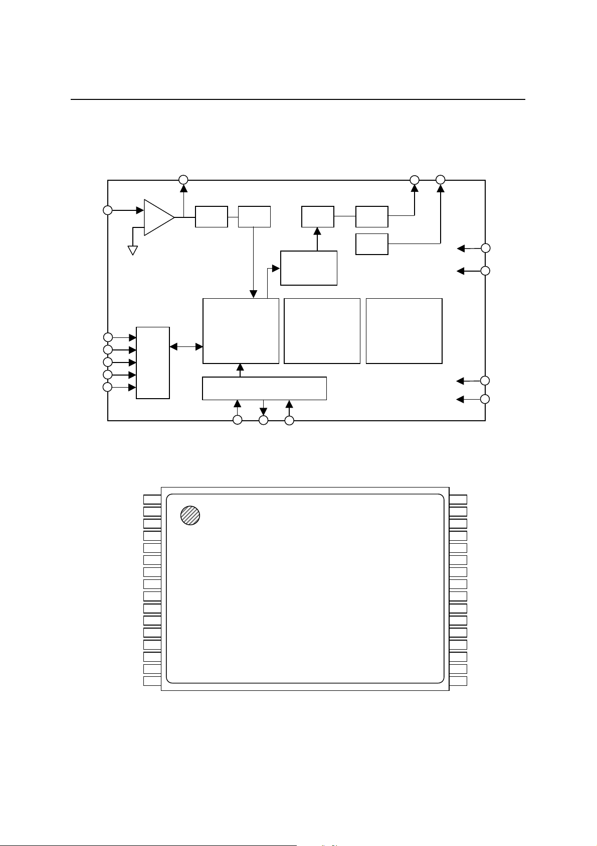
BLOCK DIAGRAM
PEDS87V1021-01
MS87V1021
LIN
CS
SI
SO
SK
BUSY
SG
MCU
I/F
LOUT
LPF
ADPCM
Analizer/
Synthesizer
Timing Controller
XT XT RESET
ADC
DAC
Volume
Controller
DARM
2M-Bit
LPF
SG
AOUT
MaskROM
512k-Bit
SG
AIN
AMON
TEST
TEST
PIN CONFIGURATION (TOP VIEW)
TEST
TEST
TEST
TEST
TEST
TEST
TEST
TEST
TEST
BUSY
SK
SO
SI
CS
MVDD
1
2
3
4
5
6
7
8
9
10
11
12
13
14
15
16
32-pin plastic TSOP Type I (TSOP32-P814-K)
MGND
32
AGND
31
SG
30
LIN
29
LOUT
28
AMON
27
AOUT
26
AIN
25
AVDD
24
DGND
23
TEST
TEST
22
21
TEST
20
RESET
19
XT
18
XT
17
DVDD
4/63
1
Semiconductor
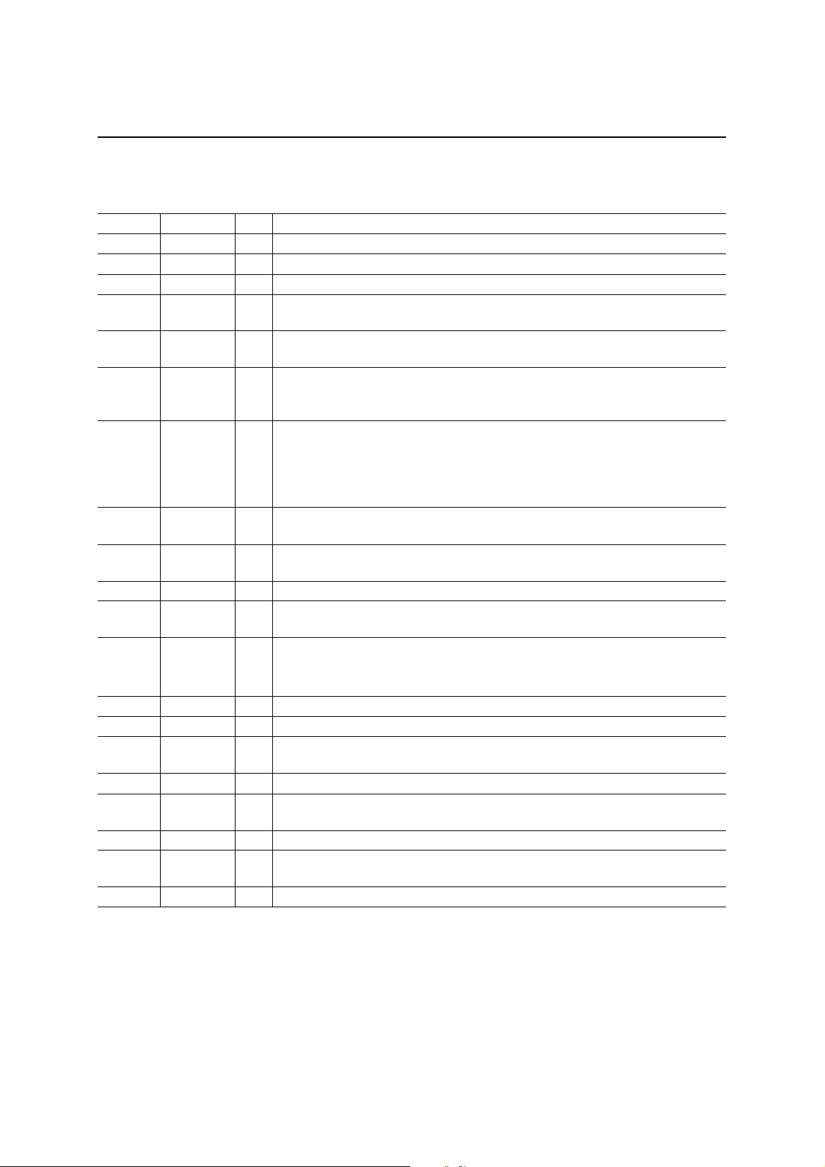
PIN DESCRIPTION
Pin No. Symbol I/O Description
14 SI I Inputs 8-bit command or data.
13 SO O Outputs 8-bit status or data.
12 SK I Data transfer clock for SI and SO.
15 CS I
11 BUSY O
19
18
20 RESET I
31 SG O
30 LIN I
29 LOUT O Output pin for internal OP amplifier
27 AOUT O
2
3-10,
21-23
28 AMON O Output pin for analog testing. Leave it unconnected.
26 AIN I Input pin for analog testing. Fix it at the GND level.
17 DVDD —
24 DGND — Digital GND pin
16 MVDD —
1 MGND — Ground pin for DRAM
25 AVDD —
32 AGND — Analog GND pin
XT
XT
TEST
TEST
The SK pulse is accepted w hen this pin i s “L”. The SK pulse is not accep ted when
this pin is “H”.
Outputs “H” level during command execution. At that time, do not input a
command from the external microcontroller.
Crystal oscillator connection pin s. When using an ex ternal cl oc k, input the clo ck
I
via the XT pin and le ave the XT pin unconn ected. When an external clock is u sed
O
in power down mode, fix the XT pin at the GND level.
The device is reset when “L” level is input. When oscillation starts, set this pin to
“L” level until oscillation becomes stable, and set to “H” level after oscillation
becomes stable. Data stored in the internal DRAM is cleared when “L” level is
input, while data is not erased when a reset signal is input for the purpose of
releasing the Pdwn1 mode.
Analog reference voltage (signal ground). Connect a 1 µF capacitor between
AGND and this pin.
Inverting input pin for internal OP amplifier. The non-inverting input pin is
internally connected to SG.
Output pin for playback LPF. This pin outputs playback waveforms and is
connected to the speaker driving amplifier.
Testing pin. The TEST pin is fixed at the V
I
the GND level.
Digital power supply pin. Connect a 0.1 µF or more bypass capacitor between
DGND and this pin.
Power supply pin for DRM. Connect a 0.1 µF or more by pas s c apa citor between
MGND and this pin.
Analog power supply pin. Connect a 0.1 µF or more bypass capacitor between
AGND and this pin.
DD
PEDS87V1021-01
MS87V1021
level and the TEST pins are fixed at
5/63
1
Semiconductor
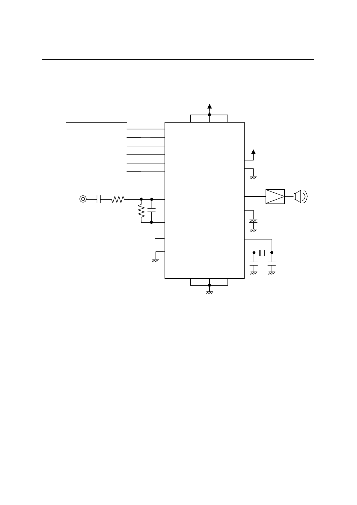
APPLICATION CIRCUIT EXAMPLE
MCU
MVDD DVDD AVDD
SI
SO
SK
CS
RESET
BUSY
PEDS87V1021-01
MS87V1021
TEST
TEST
Voice input
OPEN
MS87V1021
LIN
LOUT
AMON
AIN
MGND DGND AGND
MSC1157
AOUT
SG
XT
XT
6/63
1
Semiconductor
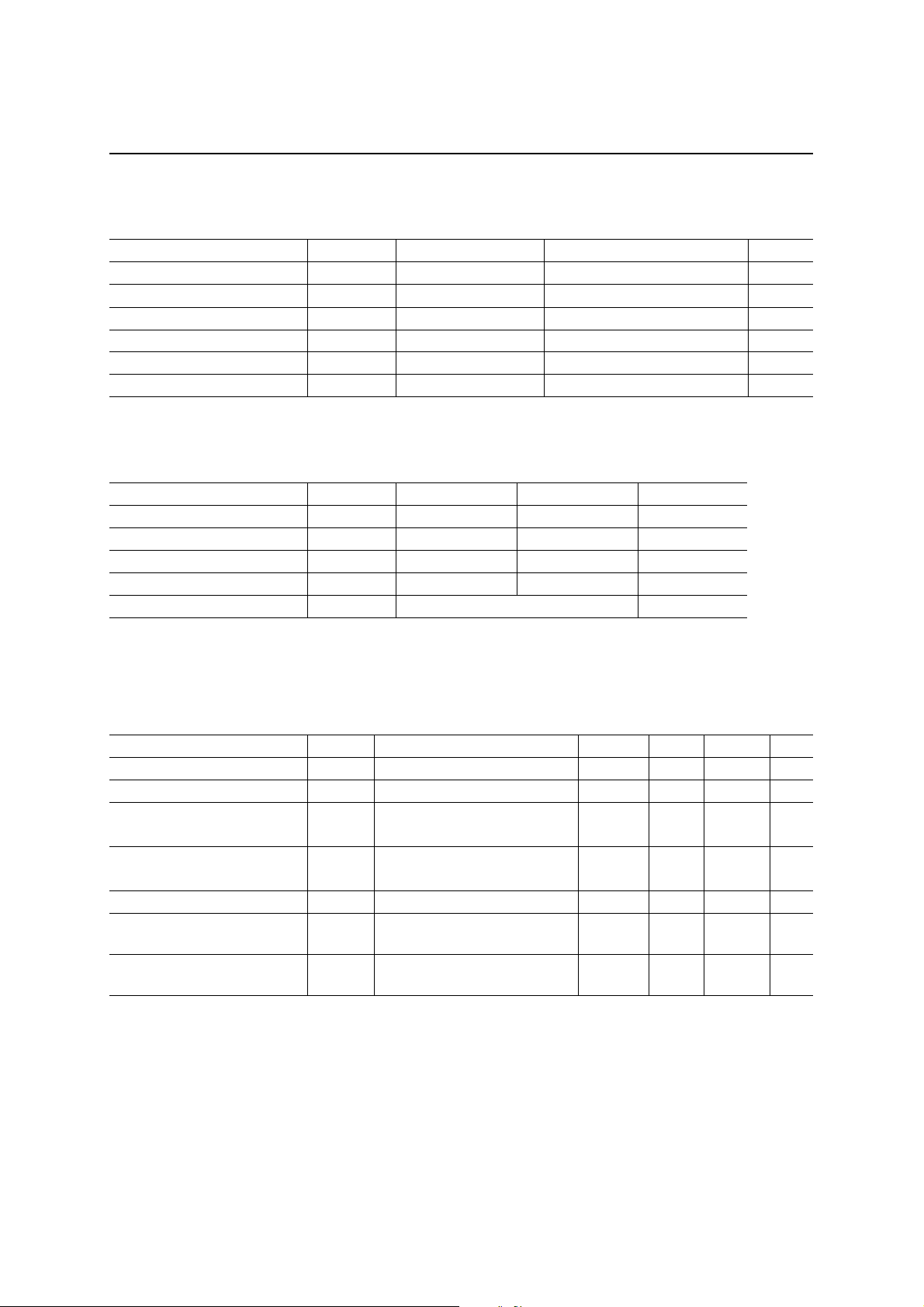
ABSOLUTE MAXIMUM RATINGS
Parameter Symbol Condition Rated value Unit
Power supply voltage V
Pin voltage V
Output shortcircuit current I
Power dissipation P
Operating temperature T
Storage temperature T
DD
T
OS
D
OPR
STG
Ta = 25°C –0.5 to 4.6 V
Ta = 25°C –0.5 to VDD+0.5 V
Ta = 25°C 50 mA
Ta = 25°C 1 W
— –20 to +70 °C
— –55 to +150 °C
RECOMMENDED OPERATING CONDITIONS
(Ta= –20 to +70°C)
Parameter Symbol Min. Max. Unit
Power supply voltage V
DD
Power supply voltage GND 0 0 V
“H” input voltage V
“L” input voltage V
Source oscillation frequency f
IH
IL
OSC
2.7 3.6 V
VDD–0.2 V
DD
–0.2 0.2 V
4.096 MHz
PEDS87V1021-01
MS87V1021
(GND = 0 V)
V
ELECTRICAL CHARACTERISTICS
DC Characteristics
Parameter Symbol Condition Min. Typ. Max. Unit
“H” output voltage V
“L” output voltage V
Input leakage current
(Note 1)
Input leakage current
(Note 2)
Operating current I
Standby current 1 I
Standby current 2 I
OH
OL
I
LI1
I
LI2
DD
DDS
DDS2
Non-measured pins are at 0 V.
Non-measured pins are at 0 V.
When powered down, no load,
When powered down, no load,
Notes: 1. Applicable to input pins excluding XT and XT.
2. Applicable to XT and XT.
IOH = –1 mA VDD–0.3 — — V
IOL = +1 mA — — 0.3 V
0 V < VIN < V
0V < VIN < V
f
= 4.096 MHz no load — 10 15 mA
OSC
with DRAM refreshing
without DRAM refreshing
(Ta = –20 to +70°C)
DD
DD
–10 — 10 µA
–20 — 20 µA
——70µA
——40µA
7/63
1
Semiconductor
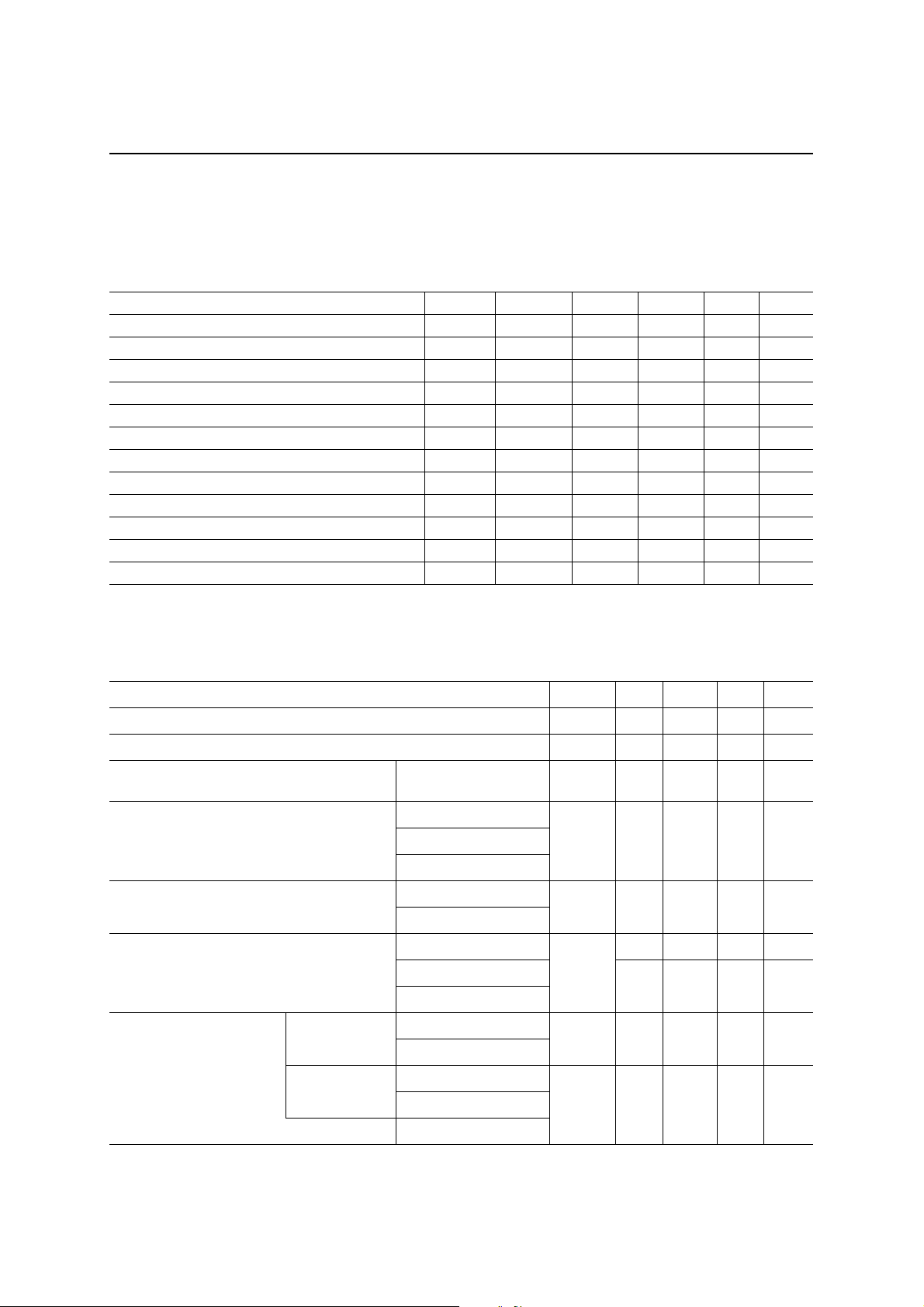
AC Characteristics
1. Microcontroller interface mode
Parameter Symbol Min. Typ. Max. Unit Note
RESET pulse width t
RESET execution time t
Setup and hold time of SK for CS t
SK pulse width “H” t
SK pulse width “L” t
Setup time of SI for SK rise t
Hold time of SI for SK rise t
Data valid time from fall of CS t
Data Hi-Z time from rise of CS t
Data valid time from fall of SK t
BUSY rise time from rise of CS t
Source oscillation duty cycle t
RST
REX
SKS
SKH
SKL
DS
DH
CSE
CSF
DD
BSY
DUTY
PEDS87V1021-01
MS87V1021
(VDD = 2.7 to 3.6 V, Ta = –20° to +70°C)
(f
= 4.096 MHz Fsam = 8.0 kHz)
OSC
1——µs1
——5ms
500 — — ns
1000 — — ns
1000 — — ns
250 — — ns
250 — — ns
— — 200 ns
— — 200 ns
— — 200 ns
— — 200 ns
40 50 60 %
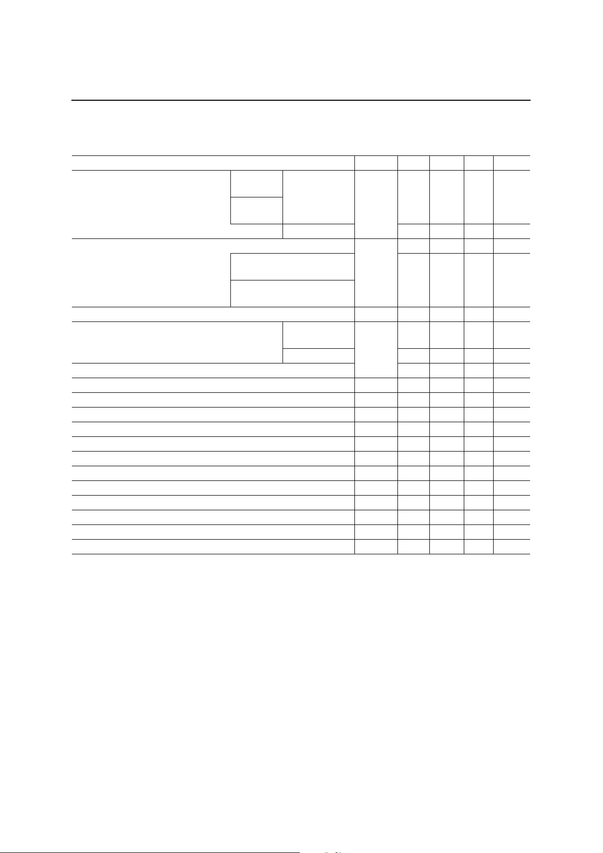
2. BUSY time when a command is executed
Parameter Symbol Min. Max. Unit Note
BUSY time after input of command t
BUSY time after input of mode setting command t
BUSY time after input of Area1 command
(3)
BUSY time after input of Area2 command
(3)
BUSY time after input of Delay command (3)
BUSY time after input of Rec command (2)
During
BUSY time after input of
recording
Play command (2)
During pause
Normal mode t
Delayed play mode
Retroactive play mode
Normal mode
Retroactive play mode
Normal mode
Delayed play mode — 65 ms 2
Retroactive play mode
Normal mode
Delayed play mode
Retroactive play mode
Delayed play mode
Retroactive play mode
Normal mode
(VDD = 2.7 to 3.6 V, Ta = –20 to +70°C)
(f
= 4.096 MHz Fsam = 8.0 kHz)
OSC
BR
MODB
AR1B
t
AR2B
t
DLYB
t
RECB
t
PLYB
t
PLYB
— 300 µs
— 300 µs
—1ms
—1ms
—1ms
—1ms
—65ms2
—1ms
8/63
1
Semiconductor
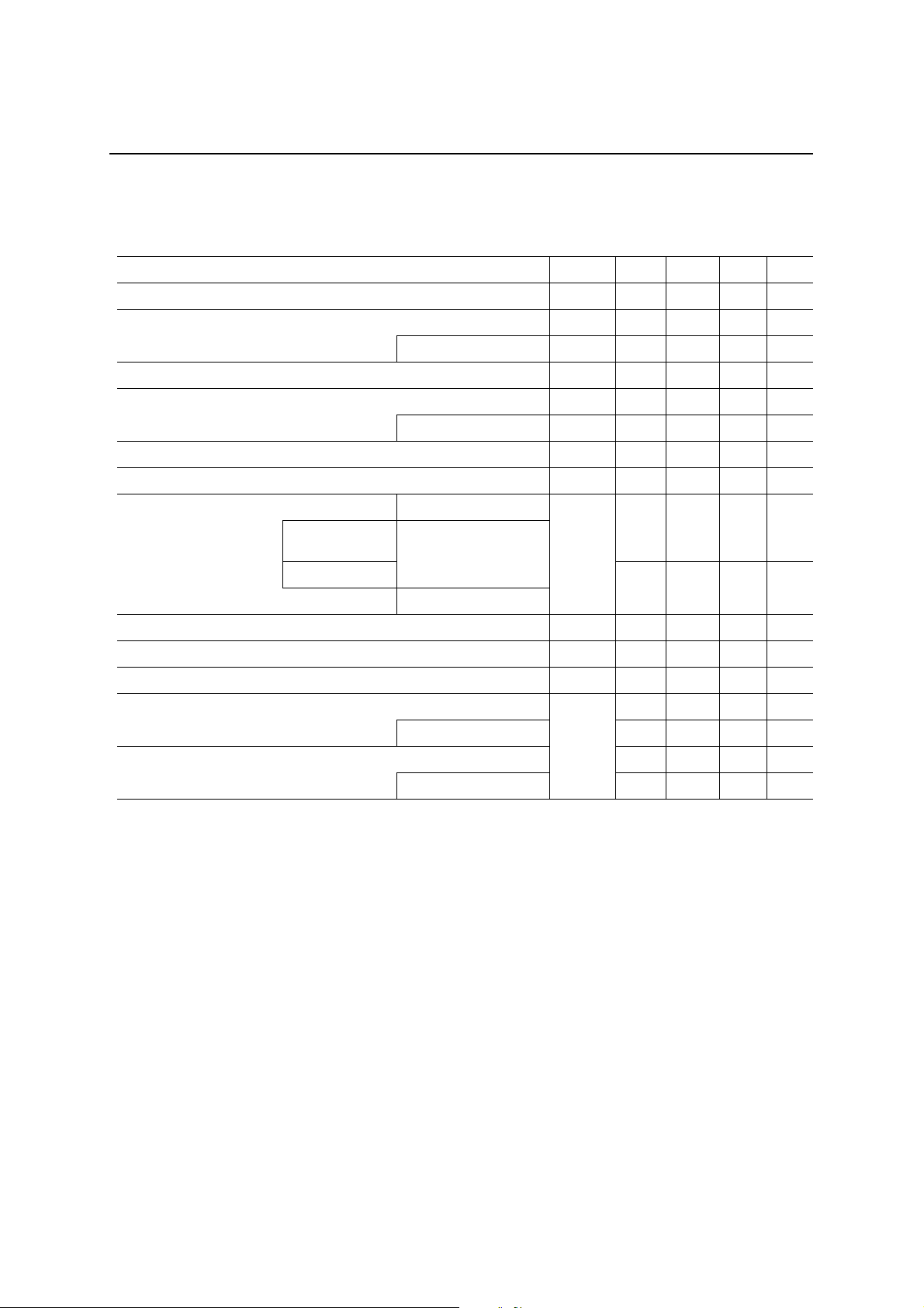
Parameter Symbol Min. Max. Unit Note
During
BUSY time after input of Play2
command (2)
recording
During
pause
Retroactive
play mode
Normal mode
BUSY time after input of Stop
command
After input of Stop command
during pause
During ROM playback
(Non-linear)
BUSY time after input of Pause command t
Retroactive
BUSY time after input of Adrrd command (2)
play mode
Normal mode — 1 ms
BUSY time after input of Adrrd command (8)
BUSY time after input of Adrwr command (8) t
BUSY time after input of Cue/Rew command (2) t
BUSY time after input of Del command (2) t
BUSY time after input of Dtrw command t
BUSY time after input of Bytew command t
BUSY time after input of Byter command t
BUSY time after input of End command t
BUSY time after input of Copy command (7) t
BUSY time after input of Vol command t
BUSY time after input of Rply command t
BUSY time after input of Status command t
BUSY time after input of Nop command t
PEDS87V1021-01
MS87V1021
(VDD = 2.7 to 3.6 V, Ta = –20 to +70°C)
(f
= 4.096 MHz Fsam = 8.0 kHz)
OSC
t
PLAYB
t
SPB
t
ADRB
ADWB
CRB
DELB
CPYB
PB
BR
BR
BR
BR
BR
BR
BR
BR
—65ms2
—1ms
—65ms2
—1ms
—65ms2
—300µs
—1ms
—1ms
—65ms2
—65ms2
—300µs
—300µs
—300µs
—300µs
—10ms
1 page
—300µs
—300µs
—300µs
—300µs
A number in parenthesis indicates the number of bytes of each command.
9/63
1
Semiconductor
3. Status flag time when a co mmand is executed
Parameter Symbol Min. Max. Unit Note
PEDS87V1021-01
MS87V1021
(VDD = 2.7 to 3.6 V, Ta = –20 to +70°C)
= 4.096 MHz Fsam = 8.0 kHz)
(f
OSC
Rec command to RPM bit set t
Play command to RPM bit set t
During ROM playback t
Play2 command to RPM bit set t
Stop command to RPM bit set t
During ROM playback t
STOP command (during pause) to RPM bit set t
Rec command to REC bit set t
RECR
PLYR
RPLYR
PLYR
SPR
RSPR
PSPR
REC
—1ms
—1ms
—2ms
—65ms2
—2ms
—1ms
—1ms
—1ms
Play command to PLY bit set Delayed play mode
During
recording
Retroactive play mode
t
PLY
—65ms2
During pausing
—1ms
Normal mode
Pause command to PAUSE bit set t
Pause command to PAUSE bit reset t
Address control time during repeated ROM playback t
PUS
PUSR
AD
—65ms2
— 300 µs
—2ms
Oscillation stop from rise of CS after input of Pwdn1 command — 65 ms
During ROM playback — 1 ms
t
Oscillation stop from rise of CS after input of Pwdn2 command — 65 ms
During ROM playback
PXT
—1ms
Note 1: When powering on or releasing the power down mode, input “L” level to the RESET pin until
crystal oscillation becomes stable. Moreover, when powering on, input again “L” level to the
RESET pin for more than t
to initialize the internal circuit.
RST
2: Depending on sampling frequency Fsam.
10/63
PEDS87V1021-01
1
Semiconductor
MS87V1021
Analog Characteristics
(V
= 2.7 to 3.6V,Ta = -20 to +70°C)
DD
Parameter Symbol Condition Min. Max. Unit
DA output relative error |V
LPF input voltage range V
OP-amp open loop gain G
OP-amp input impedance R
OP-amp load resistance R
AOUT load resistance R
|No load — 5mV
DAE
FIN
OP
INA
OUTA
AOUT
—1/4 × V
DD
fIN = 0 to 4 kHz 10 dB
—1—MΩ
— 100 — kΩ
— 100 — kΩ
3/4 × V
DD
V
Analog Input Amplifier Ciricuit
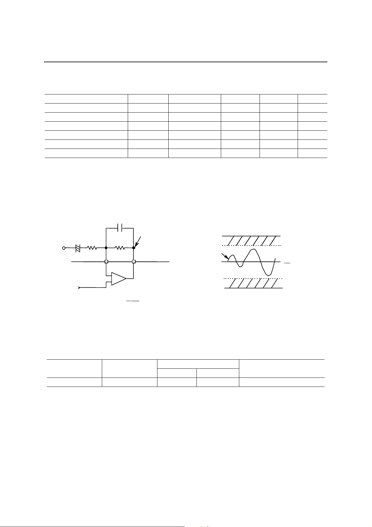
This IC contains an OP a mpl ifier with the inverti ng input pin and output pin.
The analog circuit reference voltage (signal ground) is internally input as the non-inverting input. When
amplification is required, adjust the amplification factor using an external resistor after constructing the inverting
amplifier circuit.
V
DD
V
FIN (max)
1
V
2
V
FIN (min)
GND
DD
V
IN
SG
+
Inside LSI
LIN
V
V
LO
R2R1
V
LOUT
LO
+
R2
R1
V
IH
=
LO
The output pin, LOUT, of OP amplifier is internally input to LPF (Low Pass Filter). Adjust the gain using the
external resistor so that the V
is within the accessible input voltage range V
LO
. If VLO is over the V
FIN
, the LPF
FIN
output waveform will be distorted.
The example of SCF input voltage range is shown below.
Model Supply voltage V
MS87V1021 3 V 0.75 V 2.25 V 1.5 Vp-p
SCF admissible voltage range
DD
Min. Max.
SCF admissible input voltage
The minimum value of OP-amp load resistance is 100 kΩ. The feedback resistance R2 of inverting amplifier
circuit must be larger than 100 kΩ.
11/63
PEDS87V1021-01
1
Semiconductor
MS87V1021
LPF Characteristics
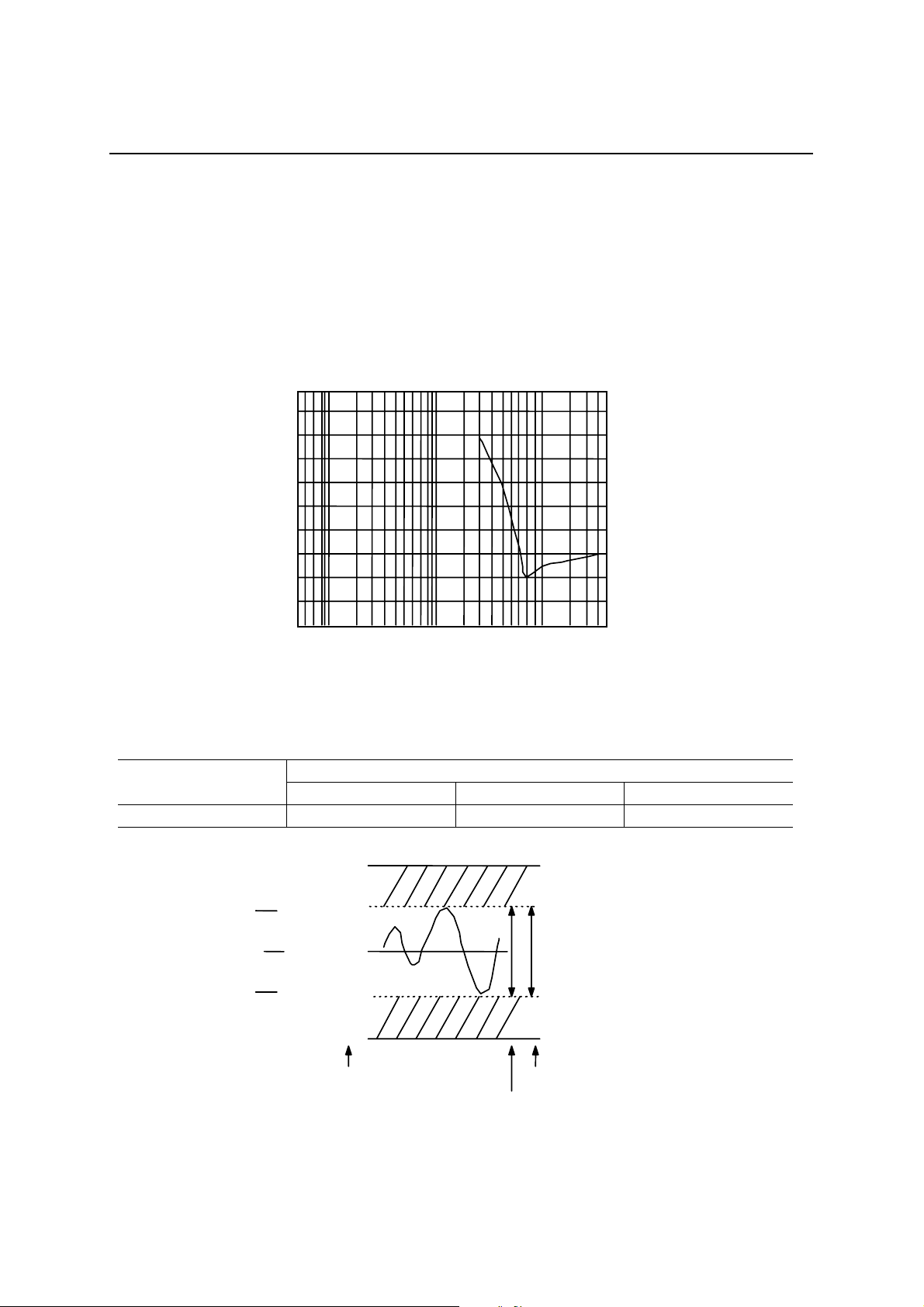
The MS87V1021 contains a 4-th order LPF in which the switched capacitor filter technique is adopted. The LOUT
pin is internally connected to the input of LPF.
The attenuation rate is –40 dB/oct. The cut-off frequency and frequency characteristics vary in proportion to
sampling fre quency (Fsam).
The cut-off frequency is designed to 4/10 of sampling frequency.
The characteristics of LPF when Fsam = 8 kHz are shown below.
[dB]
20
10
0
–10
–20
–30
–40
–50
–60
–70
–80
100 1k 10k
[Hz]
AD, DA Converter Full Scale
Model
MS87V1021 1/4 × V
3
V
DD
4
1
V
2
1
V
4
LPF characteristics (Fsam = 8.0 kHz)
AD, DA converter full scale
Min. (V) Max. (V) Amplitude (Vp-p)
DD
(3 V)
V
DD
(2.25 V)
(1.5 V)
DD
(0.75 V)
DD
0 V (0 V)
A value in parenthesis
indicates a voltage when
is 3.0 V.
V
DD
LPF admissible input voltage range
3/4 × V
DD
AD, DA converter full scale
1/2 × V
DD
12/63
PEDS87V1021-01
1
Semiconductor
MS87V1021
NOTICE
Power Supply Connection
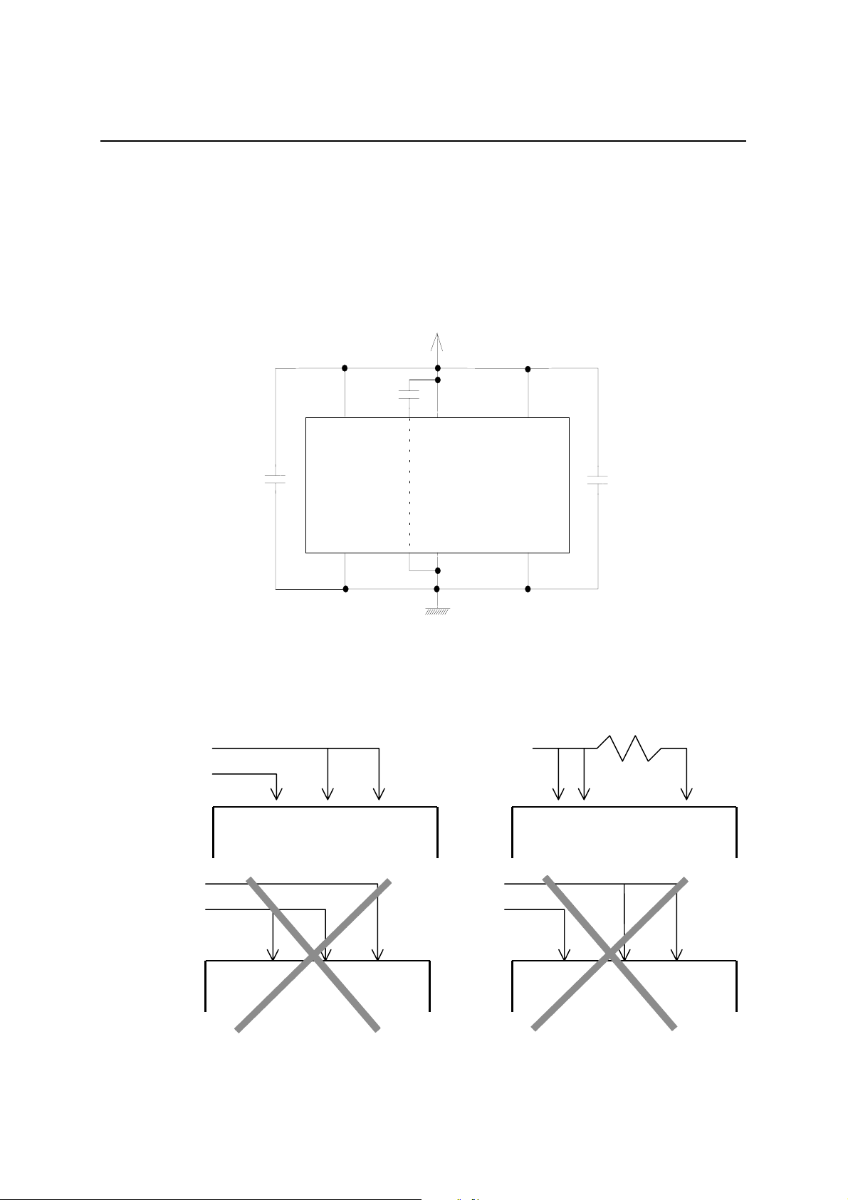
The power of this IC is supplied from a single power supply as shown below, which should be connected to the
analog section, logic section and memory section separately.
Power source
DD
MV
MGND
DD
AV
AGND
Ground
DD
DV
DGND
If the analog section, digital section and memory section are supplied from different power sources, a latch-up may
occur. Be sure to avoid the power supply connections shown below.
Power source 1
Power source 2
LSI
AVDD
MVDD
DVDD
Power source
LSI
DVDD
MVDD
AVDD
Power source 1
Power source 2
LSI
AVDD
MVDD
DVDD
Power source 1
Power source 2
LSI
MVDD
DVDD
AVDD
13/63
PEDS87V1021-01
1
Semiconductor
MS87V1021
Supplementary Explanation on SG Pin
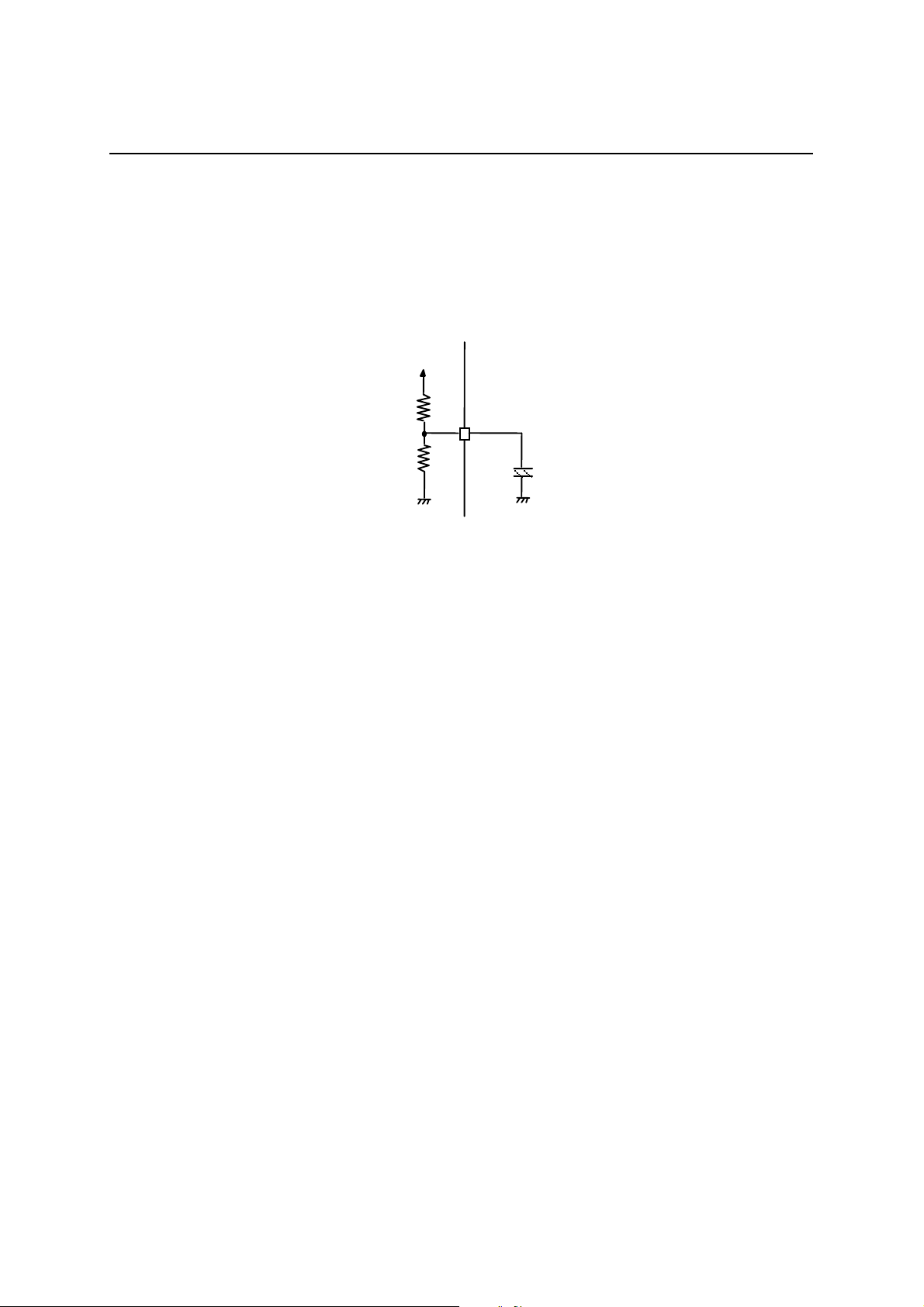
Connect a 1 µF electrolytic capacitor between the SG pin and AGND.
After reset or releasing the power down mode, do recording or playback after the voltage l evel of SG pi n becom e s
stable. The voltage level becomes stable at 1/2 of V
. The time to be stabilized is approximately 50 ms in case
DD
shown below.
Inside of LSI
Approx. 20 kΩ
Approx. 20 kΩ
External circuit
SG pin
+
1 µF
AGND
14/63
1
Semiconductor
TIMING DIAGRAMS
Serial microcontroller interface mode
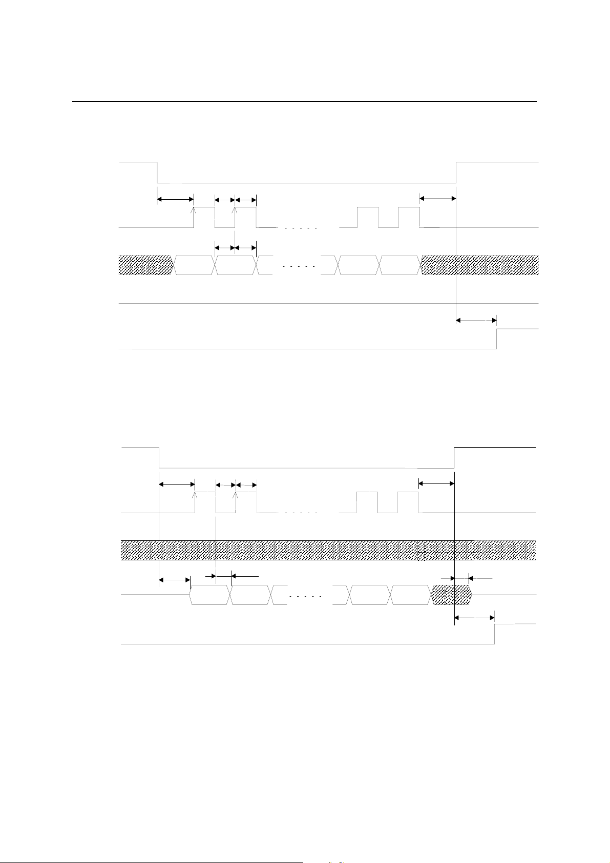
[Data write operation]
PEDS87V1021-01
MS87V1021
CS (I)
SK (I)
SI (I)
SO (O)
BUSY (O)
[Data read operation]
CS (I)
SK (I)
MSB
1st byte
D6 D5 D4
Data output
D3
Hi-Z
D2
D1
LSB
Data I/O disabled
MSB
D6
2nd byte
D5
D4
Data input
D3 D2
SI (I)
SO (O)
BUSY (O)
Hi-Z
Q6 Q5 Q4 Q3 Q2 Q1
MSB
LSB
Data I/O disabled
MSB
D6 D5 D4 D3 D2
Hi-Z
15/63
1
Semiconductor
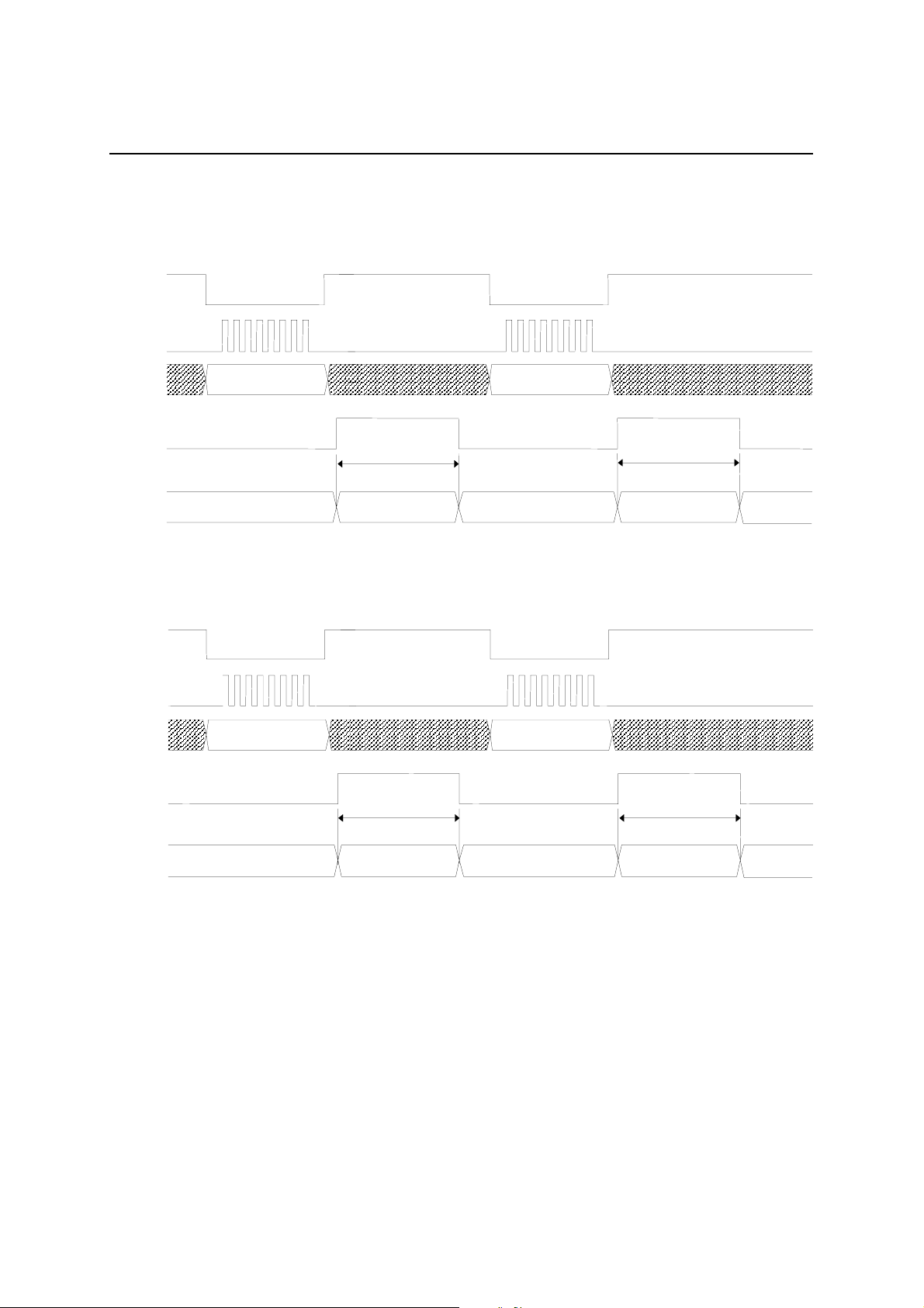
[Data write operation]
CS (I)
t
SKS
t
SKLtSKH
t
PEDS87V1021-01
MS87V1021
SKS
SK (I)
(Note) “L” level
t
t
DS
DH
SI (I)
MS
D6
SO (O)
BUSY (O)
(Note) Be sure to set SK to “L” when CS is at “H” level.
[Data read operation]
CS (I)
t
t
SKL
SKH
SK (I)
t
SKS
(Note) “L” level
Hi-Z
D1 LSB
t
SKS
(Note) “L” level
t
BSY
(Note) “L” level
SI (I)
t
DD
Q6
SO (O)
Hi-Z
t
CSE
MS
BUSY (O)
(Note) Be sure to set SK to “L” when CS is at “H” level.
D1 LSB
t
BSY
t
CSF
Hi-Z
16/63
1
(2)
S
Semiconductor
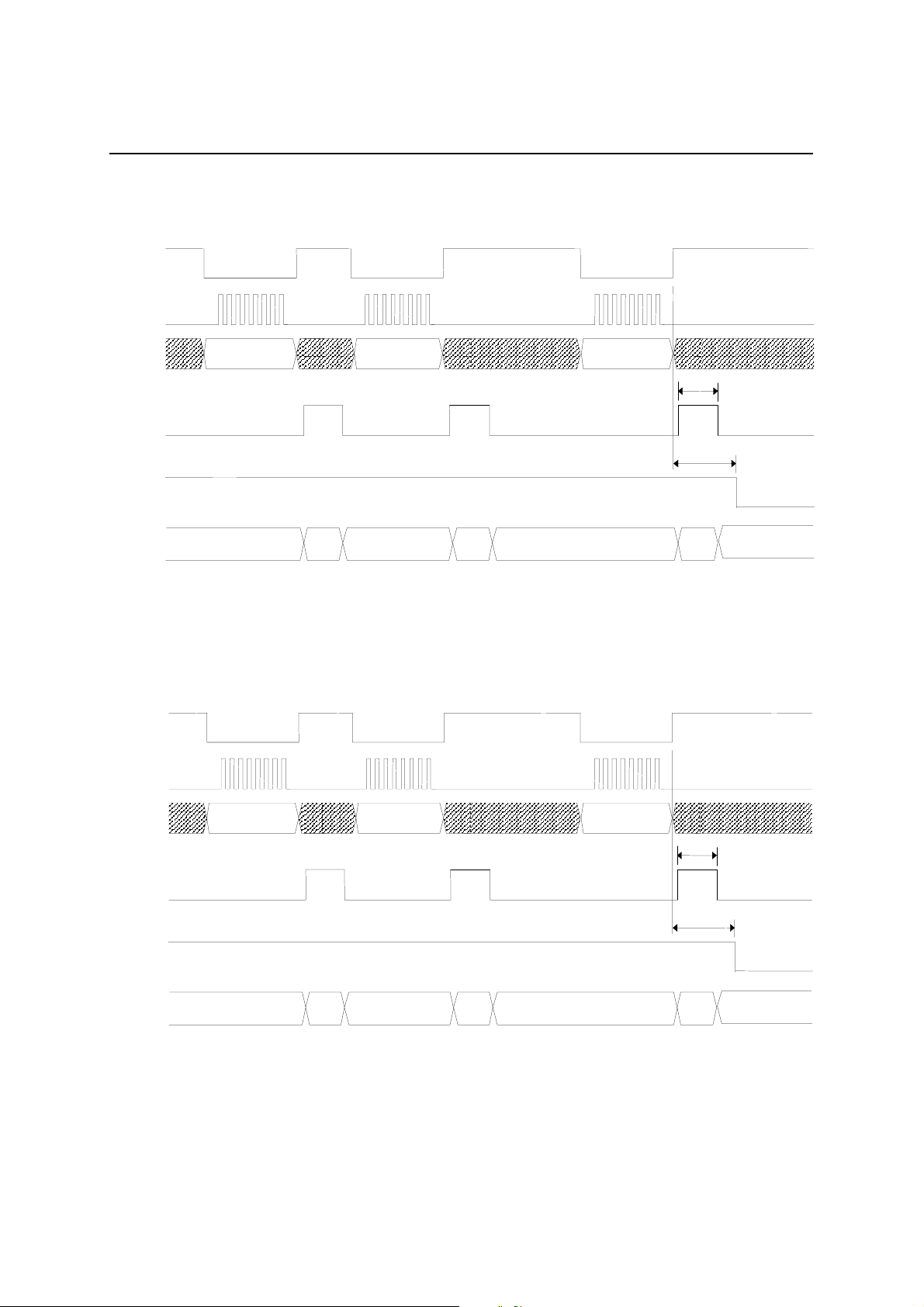
Ready for recording with Rec command
CS
SK
PEDS87V1021-01
MS87V1021
SI
Rec command (1) Rec command (2)
BUSY
Standby
Executing Rec
command (1)
Ready for playback with Play command
C
SK
SI
BUSY
Play command (1) Play command (2)
t
t
BR
Standby
t
BR
RECB
Executing Rec
command
t
PLYB
Standby
Standby
Executing Play
command (1)
Standby
Executing Play
command (2)
Standby
17/63
1
(2)
Semiconductor
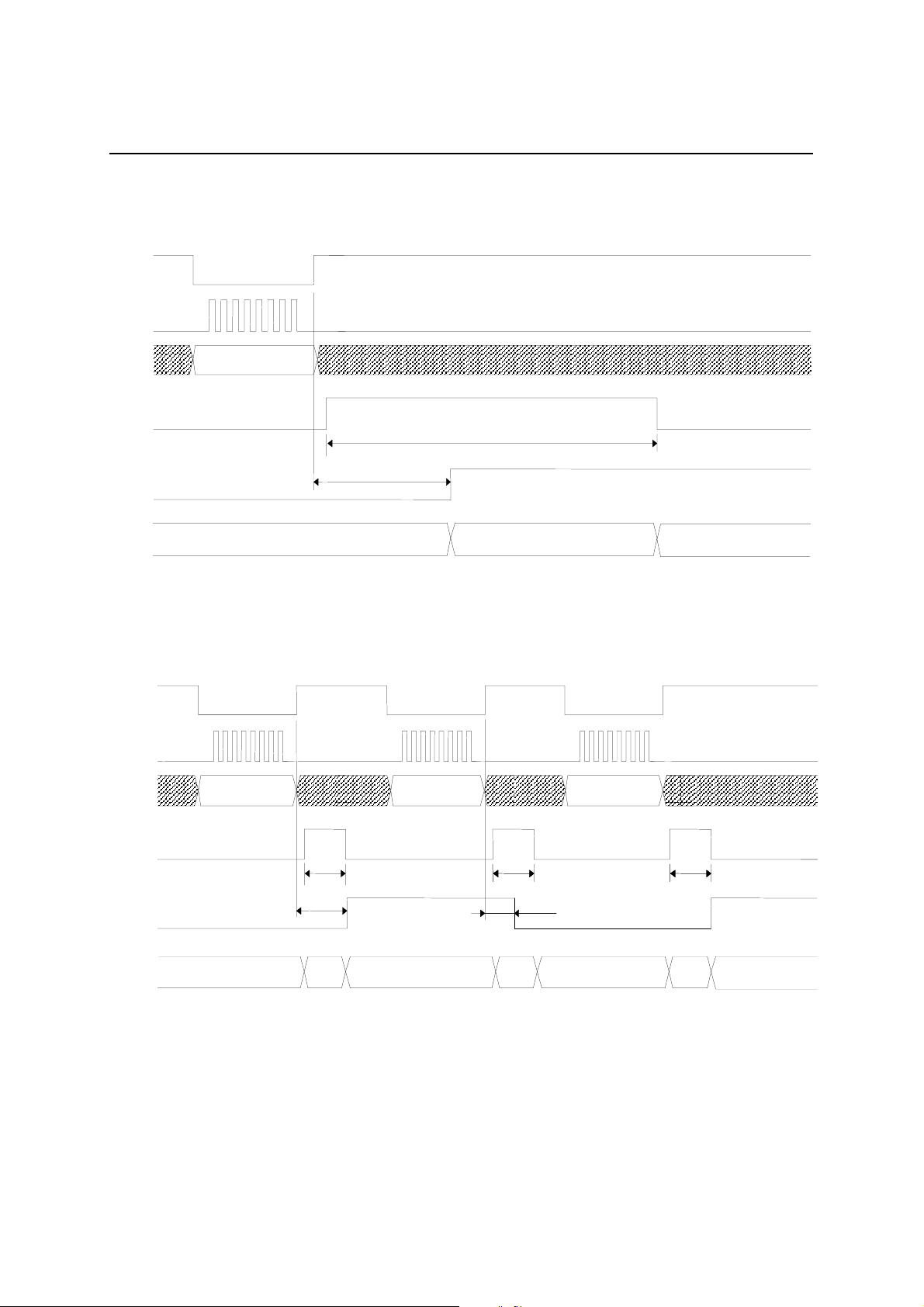
Starting recording with Start command
CS
SK
PEDS87V1021-01
MS87V1021
SI
Rec command
(1)
BUSY
RPM bit
Standby
Executing Rec
command (1)
Starting playback with Start command
CS
SK
Rec command
Standby
Executing Rec
command (2)
Start command
Standby
t
STB
t
RECR
Recording
Executing Start
command
BUSY
RPM bit
SI
Play command
(1)
Standby
Play command
Executing Play
command (1)
(2)
Standby Playing
Executing Play
command (2)
Start command
Standby
t
BR
t
PLYR
Executing Start
command
18/63
1
S
Semiconductor
Ending recording/playback with Stop command
C
SK
PEDS87V1021-01
MS87V1021
SI
Stop command (1)
BUSY
t
SPR
RPM bit
Recording/playing Stop processing
Pause of recording/playback with Pause command
CS
SK
SI
Pause command
Pause command Pause command
t
SPB
Standby
BUSY
PAUSE
bit
Recording/playing
t
PB
t
PUS
Executing Pause
command
t
PB
t
PUSR
Pausing Pausing
Recording/playing
Executing Pause
command
t
PB
Executing Pause
command
19/63
 Loading...