


查询MS52C1161A供应商
¡
MS52C1161A
131,072-Word X 8-Bit STATIC RAM +
2,097,152-Word X 8-Bit One Time PROM
DESCRIPTION
The MS52C1161A is a131,072-word by 8-bit electrically switchable 1Mb static RAM and
2,097,152-word by 8-bit electrically switchable 16Mb One Time PROM featuring 2.7V to 3.6V
power supply operation and direct LVTTL input / output compatibility. Since the circuitry is
completely static,external clocks are unnecessary,making this device very easy to use.
The MS52C1161A is packaged in 48-pin plastic TSOP and 48-pin FBGA (9mmx13mm) ,suited
for use in handy terminal and other application which required small space.
FEATURES
• 131,072-word x 8-bit configuration SRAM and 2,097,152-word x 8-bit configuration OTP
• Power supply voltage : 2.7 to 3.6V
Semiconductor
Preliminary
1998.6
• Fully static operation
• Operating temperature range : Ta= -20 to 70°C
• Access time : 100nS MAX (Vcc=2.7V)
80nS MAX (Vcc=3.0V)
• Common address inputs and data inputs / outputs for SRAM and OTP
• Input / Output LVTTL compatible
• 3-state output
• Data retention available at power supply voltage 1.5V for SRAM
• Package options :
48-pin plastic TSOP (Type II) (TSOP48-P-550-0.8) (Product : MS52C1161ATA)
48-pin plastic FBGA (FBGA48-P-0913-0.8) (Product : MS52C1161ALA)
1

MS52C1161A
PIN CONFIGURATION (TOP VIEW)
NC
A17
A15
A14
A13
A12
A11
A10
A9
CEs
VPP
GND
WE
A8
A7
A6
10
11
12
13
14
15
16
17
1
2
3
4
5
6
7
8
9
48
47
46
45
44
43
42
41
40
39
38
37
36
35
34
33
32
NC
A18
CEo
A16
I/O7
NC
I/O6
NC
I/O5
NC
I/O4
GNDVCC
VCC
NC
I/O3
NC
I/O2
A5
A4
A3
A2
A1
A0
18
19
20
21
22
23
24
48-pin TSOP (II)
31
30
29
28
27
26
25
NC
I/O1
NC
I/O0
OE
A19
A20NC
2

MS52C1161A
PIN CONFIGURATION (TOP VIEW)
A
6
5
4
3
2
1
A1
A0
A20
A19
OE CEo
BCDEFGH
A4
A3
A2
I/O0 I/O3 NC
NC
I/O1
A7
A5
NC
I/O2
NC
GND
WE
A8NC
NC
VCC GND
VCC
VPP
CEs
NC
I/O4
A9
A10A6
A11
I/O6
NC
I/O5
A12
A13
A14
A16
I/O7
NC
A15
A17
NC
A18
48-pin FBGA
Pin Name Function
A0 - A16
A17 - A20
CEs
CEo
WE
OE
I/O0 - I/O7
VCC
VPP
GND
NC
Common Address Inputs
Address Inputs for OTP
Chip Enable for SRAM
Chip Enable for OTP
Write Enable for SRAM
Common Output Enable
Common Data Inputs / Outputs
Common Power Supply
Program Power Supply for OTP
Common Ground
No Connection
3
MS52C1161A
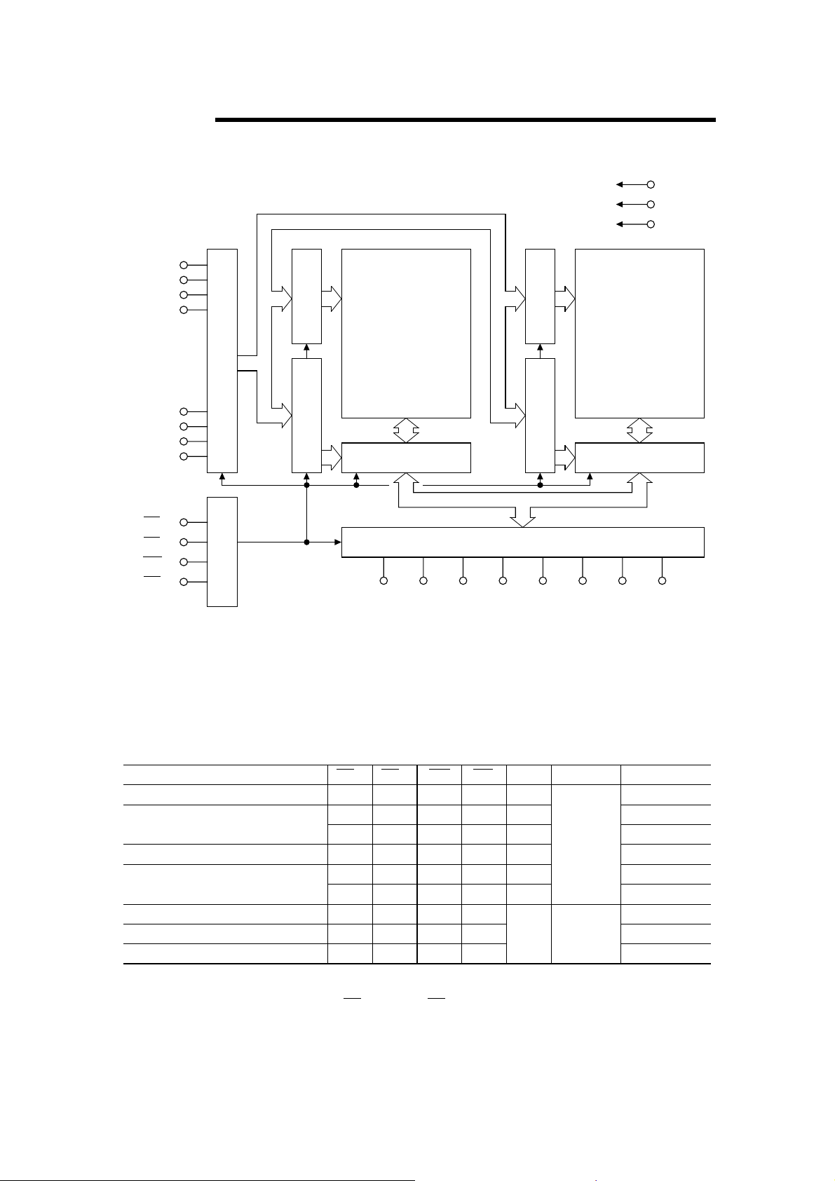
BLOCK DIAGRAM
A0
A1
A2
A3
.
.
.
.
.
.
.
.
.
.
.
.
.
.
.
.
A17
A18
A19
A20
CEo
CEs
WE
OE
Address Buffer
Control
SRAM
Memory
Row Decoder
Array
128kw x 8b
Column Decoder
I/O0 I/O1 I/O2 I/O3 I/O4 I/O5 I/O6 I/O7
Row Decoder
Column Decoder
Output Buffer
VCC
VPP
GND
OTP
Memory
Array
2Mw x 8b
MultiplexerMultiplexer
FUNCTION TABLE
Operating Mode
Standby
SRAM Read
SRAM Write
OTP Read
OTP Program Inhibit
OTP Program Verify
Note : 1. * = Don't Care ("H" or "L")
2. It is forbidden to apply CEo="L" and CEs="L" simultaneously.
CEo WE OE
CEs
H
H
H
H
H
LHH
L
L
LH
L
L
H
H
HOTP Program
H
HH
*
H
*
L
*
*
*
*
*
*
H
LD
H
H
L
VPP VCC I/O0 to I/O7
*
*
*
*
2.7V
to
3.6V
*
*
High-Z
High-Z
D
OUT
DINL
High-Z
OUT
DIN
9.75V
4.0V
High-Z
OUT
D
4

MS52C1161A
ELECTRICAL CHARACTERISTICS
Absolute Maximum Ratings
Power Supply Voltage
Input Voltage
Output Voltage
Power Dissipation
Operating Temperature
Storage Temperature
VCC
VPP
I
V
VO
PD
Topr
Tstg
Respect to GND
* -1.2VMin. for pulse width less than 30nS.
Recommended Operating Conditions
VCC
Power Supply Voltage
V
PP
GND
SRAM
Data Retention Voltage
Input High Voltage
Input Low Voltage
V
CCH
VIH
VIL
Vcc=2.7 to 3.6
Ta=25°C
Rating
-0.5 to 5.0
-0.5 to 11.5
-0.5* to Vcc+0.5
-0.5* to Vcc+0.5
0.7
-20 to 70
-55 to 125
(Ta= -20 to 70
Min. Max.Typ.
2.7 3.6
-0.5 Vcc+0.5
000
1.5 3.6
2.2
Vcc+0.5
-0.5* 0.4
UnitConditionSymbolParameter
V
V
V
V
W
°C
°C
°C)
UnitConditionSymbolParameter
V
V
V
V
V
V
* -1.2VMin. for pulse width less than 30nS.
Capacitance
Min. Max.Typ.
I=0V
Input Capacitance
Input/Output Capacitance
Note : This parameter is periodically sampled and not 100% tested.
IN
C
CI/O
V
VO=0V
(Vcc=3.3V , Ta=25°C , f=1MHz)
UnitConditionSymbolParameter
10
pF
10 pF
5

MS52C1161A
DC Characteristics (1)
Parameter Symbol Unit
Input Leakage
Current
ILI
VIN=0 to VCC
CE
Output Leakage
Current
ILO
OE=V
WE=VIL
Condition
o=VIH , CEs=VIH or
IH or
(Vcc=3.0V±0.3V,Ta=-20 to 70°C)
Min. Max.
-1.0
Typ.
1.0
1.0-1.0
VOUT=0 to VCC
I
Output High Voltage
Output Low Voltage
Standby Power
Supply Current
OH
V
VOL
ICCS
ICCS1
OH=-500µA
OL=2.1mA
I
o≥VCC-0.2V
CE
CEs≥VCC-0.2V
IN=0 to VCC
V
CEo=VIH
CEs=VIH
Vcc-0.5
0.4
10
0.3
VIN=VIH or VIL
CE
o=VIH
CEs=VIL
OE=VIH
35
VIN=VIH/VIL
TCYC=100nS
ICCA
(SRAM)
Operating Power
Supply Current
CEo≥VCC-0.2V
CE
s≤0.2V
OE≥VCC-0.2V
V
IH≥VCC-0.2V
VIL≤0.2V
TCYC=1µS
CEo=V
IL
CEs=VIH
OE=V
IH
IN=VIH/VIL
V
TCYC=100nS
10
35
ICCA*
(OTP)
CEo≤0.2V
CE
s≥VCC-0.2V
OE
≥VCC-0.2V
V
IH≥VCC-0.2V
VIL≤0.2V
TCYC=1µS
20
µA
µA
V
V
µA
mA
mA
mA
mA
mA
VPP Power
Supply Current
* Read Current
IPP
VPP=VCC
10
µA
6

MS52C1161A
DC Characteristics (2)
Parameter Symbol Unit
Input Leakage
Current
ILI
VIN=0 to VCC
CE
Output Leakage
Current
ILO
OE=V
WE=VIL
Condition
o=VIH , CEs=VIH or
IH or
(Vcc=3.3V±0.3V,Ta=-20 to 70°C)
Min. Max.
-1.0
Typ.
1.0
1.0-1.0
VOUT=0 to VCC
I
Output High Voltage
Output Low Voltage
Standby Power
Supply Current
OH
V
VOL
ICCS
ICCS1
OH=-500µA
I
OL=2.1mA
o≥VCC-0.2V
CE
CEs≥VCC-0.2V
IN=0 to VCC
V
CEo=VIH
CEs=VIH
Vcc-0.5
0.4
10
0.3
VIN=VIH or VIL
CE
o=VIH
CEs=VIL
OE=V
IH
40
VIN=VIH/VIL
TCYC=80nS
ICCA
(SRAM)
Operating Power
Supply Current
CEo≥VCC-0.2V
s≤0.2V
CE
OE≥VCC-0.2V
V
IH≥VCC-0.2V
VIL≤0.2V
TCYC=1µS
CEo=V
IL
CEs=VIH
IH
OE=V
V
IN=VIH/VIL
TCYC=80nS
15
40
ICCA*
(OTP)
CEo≤0.2V
s≥VCC-0.2V
CE
OE
≥VCC-0.2V
V
IH≥VCC-0.2V
VIL≤0.2V
TCYC=1µS
25
µA
µA
V
V
µA
mA
mA
mA
mA
mA
VPP Power
Supply Current
* Read Current
IPP
VPP=VCC
10
µA
7

MS52C1161A
SRAM AC Characteristics
SRAM Read Cycle (1)
Parameter Symbol Unit
Read Cycle Time
Address Access Time
CEs Access Time
OE Access Time
CEs to Output in Low-Z
OE to Output in Low-Z
Output Hold from Address Change
CEs to Output in High-Z
OE to Output in High-Z
SRAM Write Cycle (1)
Parameter Symbol Condition
Write Cycle Time
Address Setup Time
Write Pulse Width
Write Recovery Time
Data Setup Time
Data Hold Time
WE to Output in High-Z
CEs to End of Write
Address Valid to End of Write
Output Active from End of Write nS
tRC
tAA
tCO
tOE
tCLZ
tOLZ
tOH
tCHZ
tOHZ
tWC
tAS
tWP
tWR
tDS
tDH
tWHZ
tCW
tAW
tWLZ
Condition
(Vcc=3.0V±0.3V,Ta=-20 to 70°C)
Min. Max.
100
10
5
10
(Vcc=3.0V
Min. Max.
100
±0.3V,Ta=-20 to 70°C)
0
75
0
40
0
90
90
5
100
100
50
35
35
35
nS
nS
nS
nS
nS
nS
nS
nS
nS
Unit
nS
nS
nS
nS
nS
nS
nS
nS
nS
Test Condition
Input Pulse Levels ------------------------- 0.4V/2.4V
Input Timing Reference Levels --------- 0.8V/2.0V
Output Load --------------------------------- 50pF
Output Timing Reference Levels ------- 0.8V/2.0V
Input Rise and Fall Time ----------------- 5nS
1.85V
690
Dout
50pF
(Including scope and
jig capacitance)
8

MS52C1161A
SRAM Read Cycle (2)
Parameter Symbol Unit
Read Cycle Time
Address Access Time
CEs Access Time
OE Access Time
CEs to Output in Low-Z
OE to Output in Low-Z
Output Hold from Address Change
CEs to Output in High-Z
OE to Output in High-Z
SRAM Write Cycle (2)
Parameter Symbol Condition
Write Cycle Time
Address Setup Time
Write Pulse Width
Write Recovery Time
Data Setup Time
Data Hold Time
WE to Output in High-Z
CEs to End of Write
Address Valid to End of Write
Output Active from End of Write nS
tRC
tAA
tCO
tOE
tCLZ
tOLZ
tOH
tCHZ
tOHZ
tWC
tAS
tWP
tWR
tDS
tDH
tWHZ
tCW
tAW
tWLZ
Condition
(Vcc=3.3V±0.3V,Ta=-20 to 70°C)
Min. Max.
80
10
5
10
(Vcc=3.3V
Min. Max.
±0.3V,Ta=-20 to 70°C)
80
0
60
0
35
0
70
70
5
80
80
40
30
30
30
nS
nS
nS
nS
nS
nS
nS
nS
nS
Unit
nS
nS
nS
nS
nS
nS
nS
nS
nS
Test Condition
Input Pulse Levels ------------------------- 0.4V/2.4V
Input Timing Reference Levels --------- 0.8V/2.0V
Output Load --------------------------------- 50pF
Output Timing Reference Levels ------- 0.8V/2.0V
Input Rise and Fall Time ----------------- 5nS
1.85V
690
Dout
50pF
(Including scope and
jig capacitance)
9

MS52C1161A
SRAM Timing Diagrams
SRAM Read Cycle
A0 - A16
tRC
tAA
tCHZ
tCO
CEs
OE
I/O0 - I/O7
tCLZ
tOE
Valid Data-Out
tOHZ
tOH
tOLZ
Notes : 1. A read cycle of SRAM occurs during the overlap of CEo="H", CEs="L", OE="L" and WE="H".
2. tOHZ , tCHZ are specified by the time when DATA is floating , not defined by the output level.
SRAM Write Cycle
tWC
A0 - A16
CEs
WE
Din
Dout
tCW
tAW
tAS tWR
tWP
tDS tDH
Data-In
tWHZ tWLZ
10

MS52C1161A
Notes : 1. A write cycle of SRAM occurs during the overlap of CEo="H" , CEs="L" and WE="L".
2. OE may be either of "H" or "L" in the write cycle of SRAM.
3.
4.
5. tWR , tDS , tDH are specified from CEs="H" or WE="H" , whichever occurs first.
6. tWHZ is specified by the time when DATA output is floating , not defined by the output level.
7. When I/O pins are in the output mode , don't apply the inverted input signal to the output pins.
tAS is specified from CEs="L" or WE="L" , whichever occurs last.
tWP is an overlap time of CEs="L" and WE="L".
SRAM Data Retention Characteristics
(Ta=-20 to 70°C)
Parameter Symbol Condition Min. Typ. Max. Unit
Data Retention Power
Supply Voltage
V
CCH
CEo≥VCC-0.2V
CEs
≥VCC-0.2V
IN=0 to VCC
V
1.5
VCC=1.5V
CEo
Data Retention Power
Supply Current
Chip Deselect to Data
Retention Time
Operation
Recovery Time
ICCH
tCDR
tR
tCDR tR
≥VCC-0.2V
CEs
≥VCC-0.2V
V
IN=0 to VCC
Data Retention Mode
0
5
VCC
2.7V
V
3
µA
nS
mS
V
IH
VCCH
CEs
0V
CEs≥VCC-0.2V
11

MS52C1161A
OTP AC Characteristics (1)
OTP Read Cycle (1)
Parameter
Read Cycle Time
Address Access Time
CEo Access Time
OE Access Time
CEo to Output in High-Z
OE to Output in High-Z
Output Hold
from Address Change
OTP Read Cycle (2)
Parameter
Read Cycle Time
Address Access Time
CEo Access Time
OE Access Time
CEo to Output in High-Z
OE to Output in High-Z
Output Hold
from Address Change
(Vcc=3.0V±0.3V,Ta=-20 to 70°C)
Symbol Unit
tRC
tAA
tCO
tOE
tCHZ
tOHZ
tOH
Symbol Unit
tRC
tAA
tCO
tOE
tCHZ
tOHZ
tOH
Condition
CEo=OE=VIL
OE=VIL
CEo=VIL
OE=VIL
CEo=VIL
CEo=OE=VIL
Condition
CEo=OE=VIL
OE=VIL
CEo=VIL
OE=VIL
CEo=VIL
CEo=OE=VIL
Min. Max.
100
0
0
0
(Vcc=3.3V
±0.3V,Ta=-20 to 70°C)
Min. Max.
80
0
0
0
100
100
50
40
35
80
80
50
40
35
nS
nS
nS
nS
nS
nS
nS
nS
nS
nS
nS
nS
nS
nS
Test Condition
Input Pulse Levels ------------------------- 0.4V/2.4V
Input Timing Reference Levels --------- 0.8V/2.0V
Output Load --------------------------------- 50pF
Output Timing Reference Levels ------- 0.8V/2.0V
Input Rise and Fall Time ----------------- 5nS
1.85V
690
Dout
50pF
(Including scope and
jig capacitance)
12

MS52C1161A
OTP Timing Diagrams
OTP Read Cycle
A0 - A20
tRC
tAA
tCHZ
tCO
CEo
tOHZ
OE
tOE
I/O0 - I/O7
Notes : 1. A read cycle of OTP occurs during the overlap of CEo="L", CEs="H" and OE="L".
2. tOHZ , tCHZ are specified by the time when DATA is floating , not defined by the output level.
Valid Data-Out
tOH
OTP DC Characteristics
OTP Programming Operation
Parameter Symbol Unit
Input Leakage Current
Program
Power Supply Current
Power Supply Current
Input High Voltage
Input Low Voltage
Output High Voltage
Output Low Voltage
Program Voltage
CC Voltage
V
ILI
IPP2
ICC
VIH
VIH
VOH
VOL
VPP
VCC
Condition
VI=VCC+0.5V
CEo=VIL
OH=-500µA
I
IOL=2.1mA
(Ta=25°C±5°C)
Min. Max.
3.0
-0.5
2.4
9.5
3.9
Typ.
9.75
4.0
10
50
50
V
CC+0.5
0.8
0.45
10.0
4.1
µA
mA
mA
V
V
V
V
V
V
13

MS52C1161A
OTP AC Characteristics (2)
OTP Programming Operation
Parameter Symbol Unit
Address Setup Time
OE Setup Time
Data Setup Time
Address Hold Time
Data Hold Time
OE to Output in High-Z
PP Power Setup Time
V
Program Pulse Width
Data Valid from OE
OTP Programming Waveform
A0 - A20
tAS
(Vcc=4.0V±0.1V,VPP=9.75V±0.25V,Ta=25°C±5°C)
Min. Max.Condition Typ.
tAS
tOES
tDS
tAH
tDH
tDFP
tVS
tPW
2
2
2
0
2
0
2
10
tOE
tPW
130
119
150
tAH
µS
µS
µS
µS
µS
nS
µS
µS
nS
o
CE
tOES
OE
tDHtDS
tCE
I/O0 - I/O7
DIN
tVS
Vpp
Program
Note : When OTP is programming mode , CEs should be "H" level.
Program Verify
tDFP
DOUT
14

MS52C1161A
Pin Check Function
Pin Check Function is to check contact between each device-pin and each socket-lead with EPROM
programmer.
Setting up address as the following condition call the preprogrammed codes on device outputs.
A0
0
1
A1
1
0
A2 A3
0
1
A4
10
0
1
A5 A6
1
0
A7
010VH* 0
1
0
A8 A9
1
VH*
A10
1
(Vcc=3.3V
A11 A12
1
0
A13
01010011
1
0
±0.3V,CEo=V
A14 A15
1
0
A17
1
A18 A19
10
,Ta=25°C±5°C)
IL
DATA
A20
0
* :VH=8V
00
FF
15

MS52C1161A
OTP Programming / Verify Flow Chart
Programming
Bad Insertion
Increment Address
Start
NO
Pin Check
Address = First location
VCC=4.0V
VPP=9.75V
Program 10µs
NO
Last Address ?
YES
OK
Verify
Start
Pin Check
OK
Address = First location
VCC=3.0V
V
=3.0V
PP
Verify (One Byte)
PASS
V
=3.6V
CC
V
=3.6V
PP
Verify (One Byte)
NO
Bad Insertion
NG
NG
Increment Address
Address = First location
X=0
Verify (One Byte)
PASS
NO
Last Address ?
YES
VCC=3.0V
V
=3.0V
PP
Verify (One Byte)
PASS
PASS
Device Passed Device Failed
NG
X=X+1
YES
X=5?
NO
Program 10µs
NG
Device Passed
Device Failed
16

Semiconductor
NOTICE
The information contained herein can change without notice owing to product and/or technical improvements. Before using the product, please make sure that the information being referred to is up-todate.
The outline of action and examples for application circuits described herein have been chosen as an
explanation for the standard action and performance of the product. When planning to use the product,
please ensure that the external conditions are reflected in the actual circuit, assembly, and program
designs.
When designing your product, please use our product below the specified maximum ratings and within
the specified operating ranges including, but not limited to, operating voltage, power dissipation, and
operating temperature.
Oki assumes no responsibility or liability whatsoever for any failure or unusual or unexpected operation resulting from misuse, neglect, improper installation, repair, alteration or accident, improper handling, or unusual physical or electrical stress including, but not limited to, exposure to parameters beyond the specified maximum ratings or operation outside the specified operating range.
Neither indemnity against nor license of a third party’s industrial and intellectual property right, etc. is
granted by us in connection with the use of the product and/or the information and drawings contained
herein. No responsibility is assumed by us for any infringement of a third party’s right which may result
from the use thereof.
The products listed in this document are intended for use in general electronics equipment for commercial applications (e.g., office automation, communication equipment, measurement equipment, consumer
electronics, etc.). These products are not authorized for use in any system orapplication that requires
special or enhanced quality and reliability characteristics nor in any system or application where the
failure of such system or application may result in the loss or damage of property, or death or injury to
humans. Such applications include, but are not limited to, traffic and automotive equipment, safety devices, aerospace equipment, nuclear power control, medical equipment, and life-support systems.
Certain products in this document may need government approval before they can be exported to particular countries. The purchaser assumes the responsibility of determining the legality of export of these
products and will take appropriate and necessary steps at their own expense for these.
No part of the contents cotained herein may be reprinted or reproduced without our prior permission.
All brand, company and product names are the trademarks or registered trademarks of their respective
owners.
Copyright 1998 Oki Electric Industry Co., Ltd.

ADDRESSES & SEMICONDUCTOR WEB SITES
OKI Electric Industry Co., Ltd.OKI Electric Industry Co., Ltd.
OKI Electric Industry Co., Ltd.,
OKI Electric Industry Co., Ltd.OKI Electric Industry Co., Ltd.
Device Business Group,
10-3, Shibaura, 4-chome,
Minato-ku, Tokyo 108, Japan,
Tel.: +81-(0)3-5445-6327,
Fax.: +81-(0)3-5445-6328,
http://www.oki.co.jp/OKI/DBG/english/index.htm
(NOTE: URL is case sensitive)
OKI Semiconductor GroupOKI Semiconductor Group
OKI Semiconductor Group,
OKI Semiconductor GroupOKI Semiconductor Group
785 North Mary Avenue,
Sunnyvale, CA 94086, U.S.A.,
Tel.: +1-408-720-1900,
Fax.: +1-408-720-1918,
http://www.okisemi.com/
OKI Electric Europe GmbHOKI Electric Europe GmbH
OKI Electric Europe GmbH,
OKI Electric Europe GmbHOKI Electric Europe GmbH
Head Office Europe,
Hellersbergstrasse 2,
D-41460 Neuss, Germany,
Tel: +49-2131-15960,
Fax: +49-2131-103539,
http://www.oki-europe.de/
OKI Electronics (Hong Kong) Ltd.OKI Electronics (Hong Kong) Ltd.
OKI Electronics (Hong Kong) Ltd.,
OKI Electronics (Hong Kong) Ltd.OKI Electronics (Hong Kong) Ltd.
Suite 1901-1&19, Tower 3,
China Hong Kong City,
33 Canton Road, Tsimshatsui,
Kowloon, Hong Kong,
Tel.: +852-2-736-2336,
Fax.: +852-2-736-2395
OKI Semiconductor (Asia) Pte. Ltd.OKI Semiconductor (Asia) Pte. Ltd.
OKI Semiconductor (Asia) Pte. Ltd.,
OKI Semiconductor (Asia) Pte. Ltd.OKI Semiconductor (Asia) Pte. Ltd.
78 Shenton Way 09-01,
Singapore 0207,
Tel.: +65-221-3722,
Fax.: +65-323-5376
OKI Semiconductor (Asia) Pte. Ltd.OKI Semiconductor (Asia) Pte. Ltd.
OKI Semiconductor (Asia) Pte. Ltd.,
OKI Semiconductor (Asia) Pte. Ltd.OKI Semiconductor (Asia) Pte. Ltd.
Taipei Branch,
7th Fl. No.260, Tun Hwa North Road,
Taipei, Taiwan, R.O.C.,
Sumitomo-Flysun Building,
Tel.: +886-2-2719-2561,
Fax.: +886-2-2715-2892
http://www.oki.net.tw/
For further information, please contact:
People To People Technology
 Loading...