


查询MR27V802D供应商
¡
Semiconductor
MR27V802D
524,288-Word x 16-Bit or 1,048,576-Word x 8-Bit One Time PROM
DESCRIPTION
The MR27V802D is a 8Mbit electrically Programmable Read-Only Memory whose configuration can
be electrically switched between 524,288 word x 16bit and 1,048,576 word x 8bit. The MR27V802D
operates on a single +3V-3.3V power supply and is TTL compatible. Since the MR27V802D
operates asynchronously , external clocks are not required , making this device easy-to-use. The
MR27V802D is suitable as large-capacity fixed memory for microcomputers and data terminals. It is
manufactured using a CMOS double silicon gate technology and is offered in 42-pin DIP, 44-pin
SOP or 44-pin TSOP packages.
FEATURES
• 524,288 word x 16bit / 1,048,576 word x 8bit electrically switchable configuration
• Single +3V-3.3V power supply
• Access time 100ns access time (Vcc=+3V)
80ns access time (Vcc=+3.3V)
• Input / Output TTL compatible
• Three-state output
• Packages
42-pin plastic DIP (DIP42-P-600-2.54) (Product name : MR27V802DRA)
44-pin plastic SOP (SOP44-P-600-1.27-K) (Product name : MR27V802DMA)
44-pin plastic TSOP (TSOP II 44-P-400-0.80-K) (Product name : MR27V802DTP)
1A
November 1999
1/11
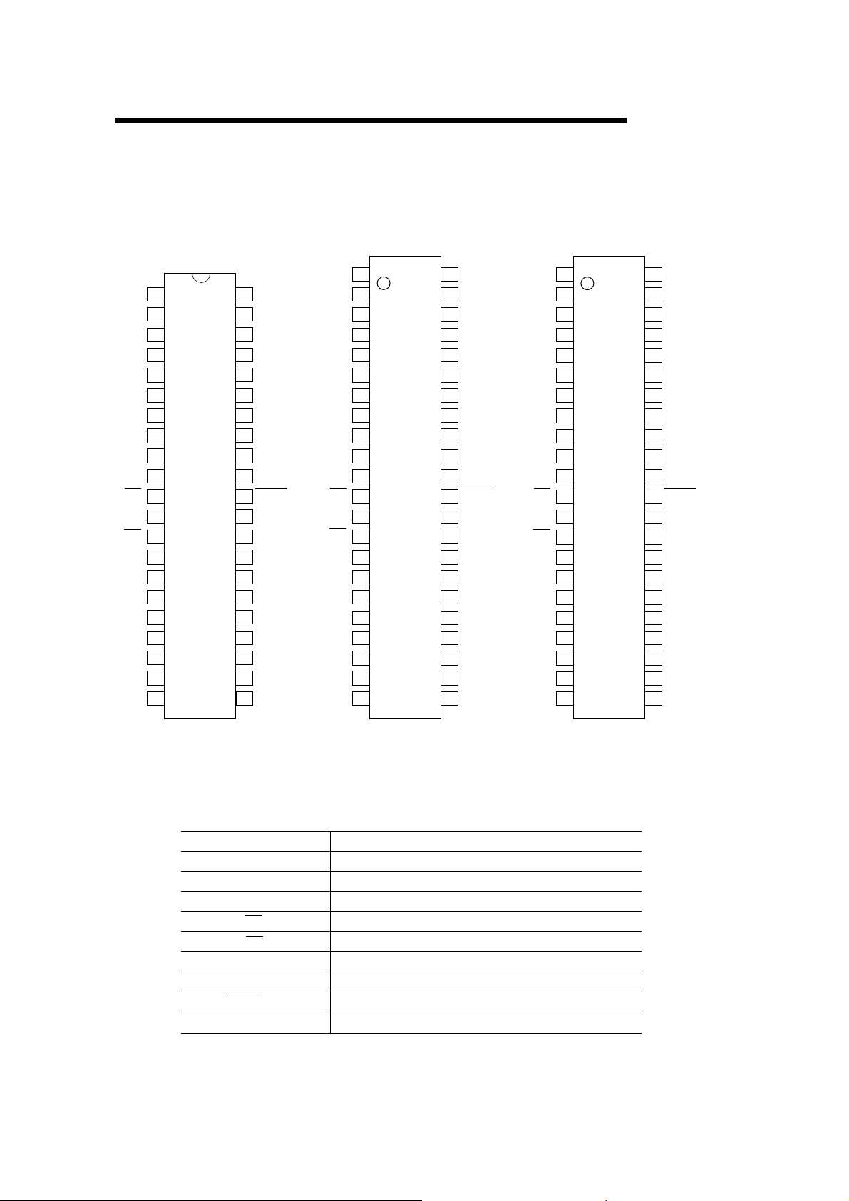
PIN CONFIGURATION (TOP VIEW)
MR27V802D
A18
A17
A7
A6
A5
A4
A3
A2
A1
A0
CE
V
SS
OE
D0
D8
D1
D9
D2
D10
D3
D11
10
11
12
13
14
15
16
17
18
19
20
21
NC
1
NC
1
2
3
4
5
6
7
8
9
42
A8
41
A9
40
A10
39
A11
38
A12
37
A13
36
A14
35
A15
34
A16
33
BYTE/Vpp
32
V
31
SS
D15/A-1
30
D7
29
D14
28
D6
27
D13
26
D5
25
D12
24
D4
23
V
22
CC
A18
A17
A7
A6
A5
A4
A3
A2
A1
A0
CE
V
SS
OE
D0
D8
D1
D9
D2
D10
D3
D11
2
3
4
5
6
7
8
9
10
11
12
13
14
15
16
17
18
19
20
21
NC
44
NC
43
A8
42
A9
41
A10
40
A11
39
A12
38
A13
37
A14
36
A15
35
A16
34
BYTE/Vpp
33
V
32
SS
D15/A-1
31
D7
30
D14
29
D6
28
D13
27
D5
26
D12
25
D4
24
V
2322
CC
NC
A18
A17
A7
A6
A5
A4
A3
A2
A1
A0
CE
V
SS
OE
D0
D8
D1
D9
D2
D10
D3
D11
10
11
12
13
14
15
16
17
18
19
20
21
NC
1
2
3
4
5
6
7
8
9
44
NC
43
A8
42
A9
41
A10
40
A11
39
A12
38
A13
37
A14
36
A15
35
A16
34
BYTE/Vpp
33
V
32
SS
D15/A-1
31
D7
30
D14
29
D6
28
D13
27
D5
26
D12
25
D4
24
V
2322
CC
42-pin DIP
PIN NAMES
FUNCTIONS
D15/A-1 Data output / Address input
A0-A18 Address input
D0-D14 Data output
CE
OE
V
CC
V
SS
BYTE/V
NC
PP
Chip enable
Output enable
Power supply voltage
GND
Mode switch / Program power supply voltage
Non connection
44-pin TSOP (II)44-pin SOP
2/11
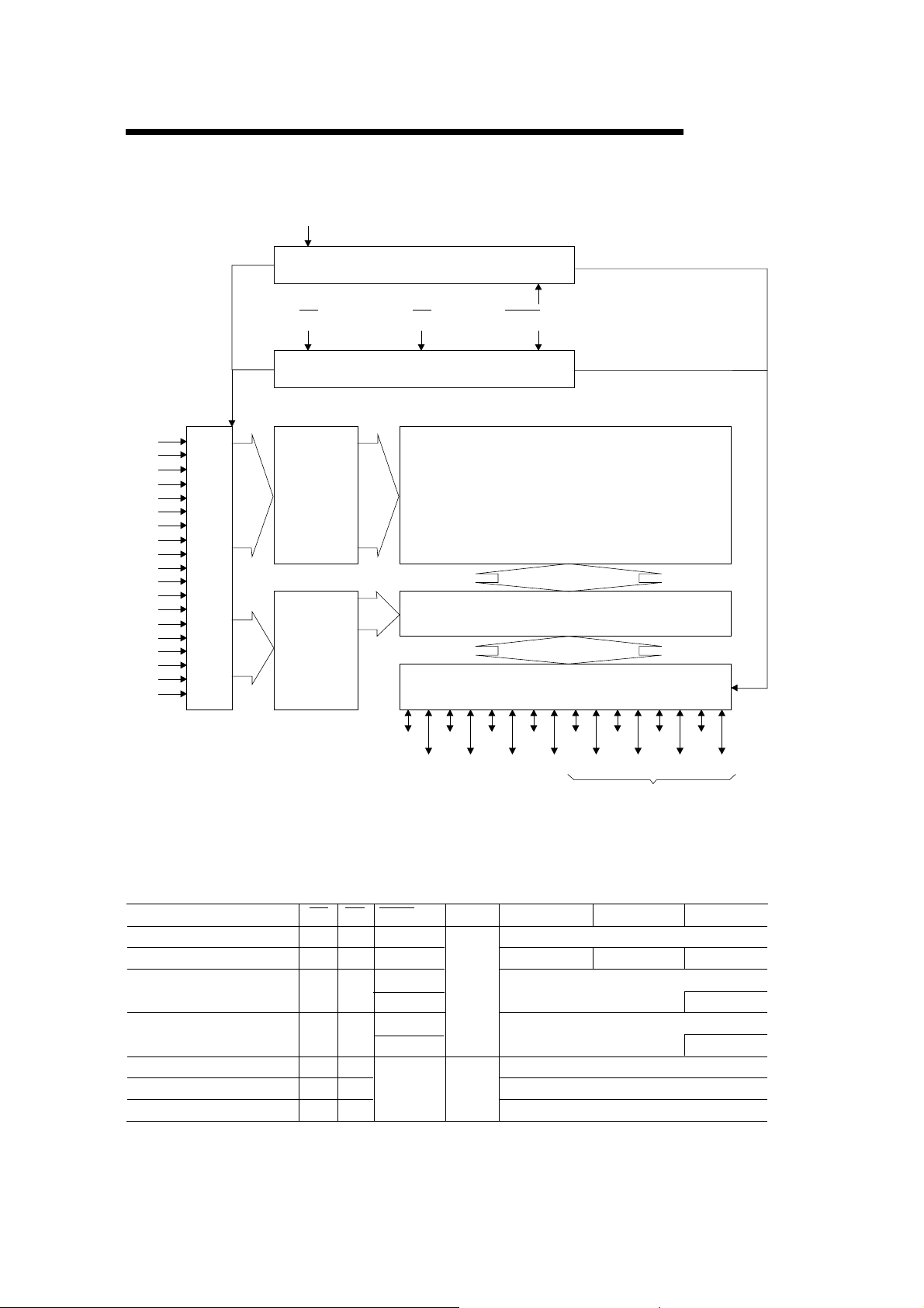
BLOCK DIAGRAM
MR27V802D
A-1
X8/X16 Switch
A0
A1
A2
A3
A4
A5
A6
A7
A8
A9
A10
A11
A12
A13
A14
A15
A16
A17
A18
Address Buffer
CE BYTE/V
OE
CE PGMOE
Memory Matrix
Row Decoder
524,288X16-Bit or 1,048,576X8-Bit
Multiplexer
Output Buffer
Column Decoder
D0
D1D2D3D4D5D6D7D8D9
PP
D10
D11
D12
D13
D14
D15
FUNCTION TABLE
MODE
READ (16-Bit)
READ (8-Bit)
OUTPUT DISABLE
STAND-BY
PROGRAM
PROGRAM INHIBIT
PROGRAM VERIFY
*: Don't Care
In 8-bit output mode, these pins are
three-stated and pin D15 functions
as the A-1 address pin.
CE OE
LL
L
L
H
L
H
*
BYTE/V
H
L
H
L
H
L
LH
H H Hi-Z
9.75V
HL
PP
V
CC
3.0V
to
3.3V
4.0V
D8 - D14D0 - D7
D
D
OUT
Hi-Z
Hi-Z
Hi-Z
D
D
D15/A-1
OUT
L/H
*
*
IN
OUT
3/11
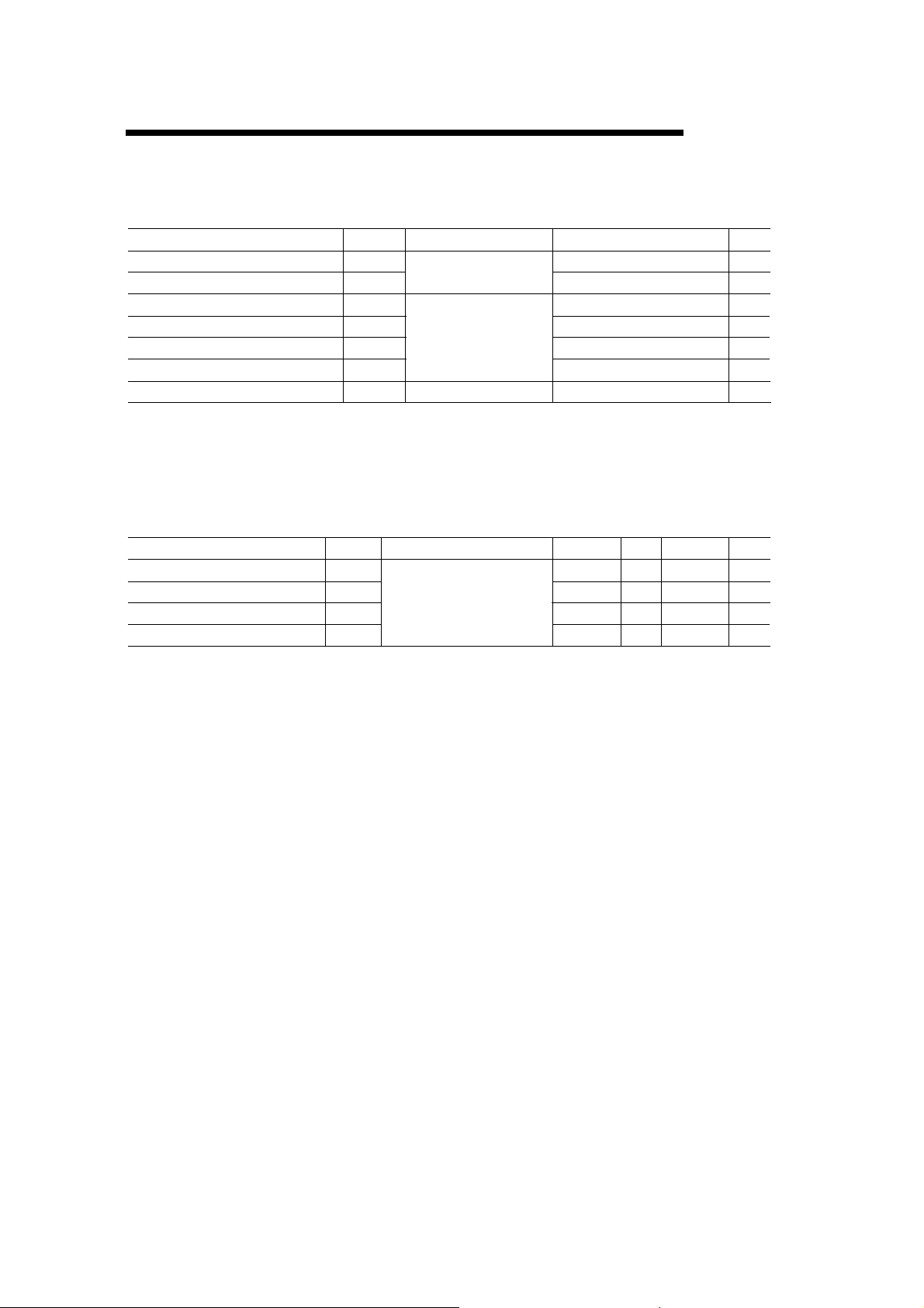
ABSOLUTE MAXIMUM RATINGS
MR27V802D
Parameter
Operating temperature under bias
Storage temperature
Input voltage
Output voltage
Power supply voltage
Program power supply voltage
Power dissipation per package
Symbol
Topr
T
stg
V
I
V
O
V
CC
V
PP
P
D
-
relative to V
-
SS
RECOMMENDED OPERATING CONDITIONS
Parameter Symbol
VCC power supply voltage
VPP power supply voltage
Input "H" level
Input "L" level
V
CC
V
PP
V
IH
V
IL
Voltage is relative to Vss
* : Vcc+1.5V (Max.) when pulse width of overshoot is less than 10nS.
** : -1.5V (Min.) when pulse width of undershoot is less than 10nS.
Condition
VCC=2.7V-3.6V
0 to 70
-55 to 125
+ 0.5
CC
(Ta=0 to 70°C)
Min. Max.
2.7
-0.5
Typ.
-
-
-
-
3.6
+0.5
V
CC
+0.5*2.2
V
CC
0.6-0.5**
UnitValueCondition
°C
°C
V-0.5 to V
V-0.5 to VCC +0.5
V-0.5 to 5
V-0.5 to 11.5
W1.0
Unit
V
V
V
V
4/11
 Loading...