

OKI MR27V801DTA, MR27V801DMA, MR27V801DRA Datasheet

1/10
¡
The MR27V801D is a 8Mbit electrically Programmable Read-Only Memory organized as 1,048,576
word x 8bit. The MR27V801D operates on a single +3V-3.3V power supply and is TTL compatible.
Since the MR27V801D operates asynchronously , external clocks are not required , making this
device easy-to-use. The MR27V801D is suitable as large-capacity fixed memory for microcomputers
and data terminals. It is manufactured using a CMOS double silicon gate technology and is offered
in 32-pin DIP, 32-pin SOP or 32-pin TSOP packages.
1A
MR27V801D
1,048,576-Word x 8-Bit One Time PROM
DESCRIPTION
FEATURES
• 1,048,576 word x 8bit
• Single +3V-3.3V power supply
• Access time 100ns access time (Vcc=+3V)
80ns access time (Vcc=+3.3V)
• Input / Output TTL compatible
• Three-state output
• Packages
32-pin plastic DIP (DIP32-P-600-2.54) (Product name : MR27V801DRA)
32-pin plastic SOP (SOP32-P-525-1.27-K) (Product name : MR27V801DMA)
32-pin plastic TSOP (TSOP I 32-P-814-0.50-K) (Product name : MR27V801DTA)
Semiconductor
November 1999
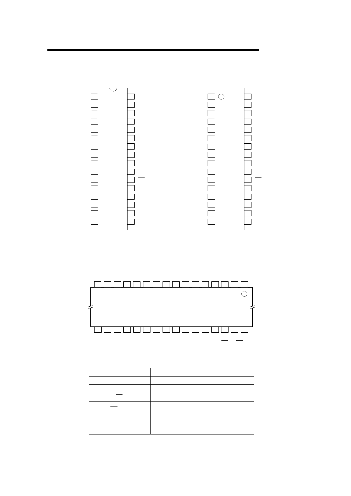
PIN CONFIGURATION (TOP VIEW)
MR27V801D
2/10
PIN NAMES
FUNCTIONS
A0 - A19 Address input
D0 - D7 Data output
CE
Output enable /
Program power supply voltage
V
CC
Power supply voltage
OE/V
PP
Chip enable
V
SS
GND
A19
A18
A17
A13
A8
A9
A11
D6
D5
D4
D3
A14
32
31
30
2
3
4
5
29
28
27
26
6
7
8
9
25
24
23
22
10
11
12
13
21
20
19
18
14
15
16 17
A16
A7
A6
A5
A4
A3
A2
D1
D2
1
CE
A15
A12
A1
A0
D0
V
SS
V
CC
OE/Vpp
A10
D7
32-pin DIP
A19
A18
A17
A13
A8
A9
A11
D6
D5
D4
D3
A14
32
31
30
2
3
4
5
29
28
27
26
6
7
8
9
25
24
23
22
10
11
12
13
21
20
19
18
14
15
16 17
A16
A7
A6
A5
A4
A3
A2
D1
D2
1
CE
A15
A12
A1
A0
D0
V
SS
V
CC
OE/Vpp
A10
D7
32-pin SOP
A19 A18
A17
A13A8A9
A11A14
A16
A7
A6
A5
A4
A3
A2 D1
D2
CE
A15
A12
A1
A0
D0
V
SS
V
CC
OE/Vpp
A10
32-pin TSOP
32313029282726252423222120191817
12345678910111213141516
D3 D5 D7
D4 D6
3/10
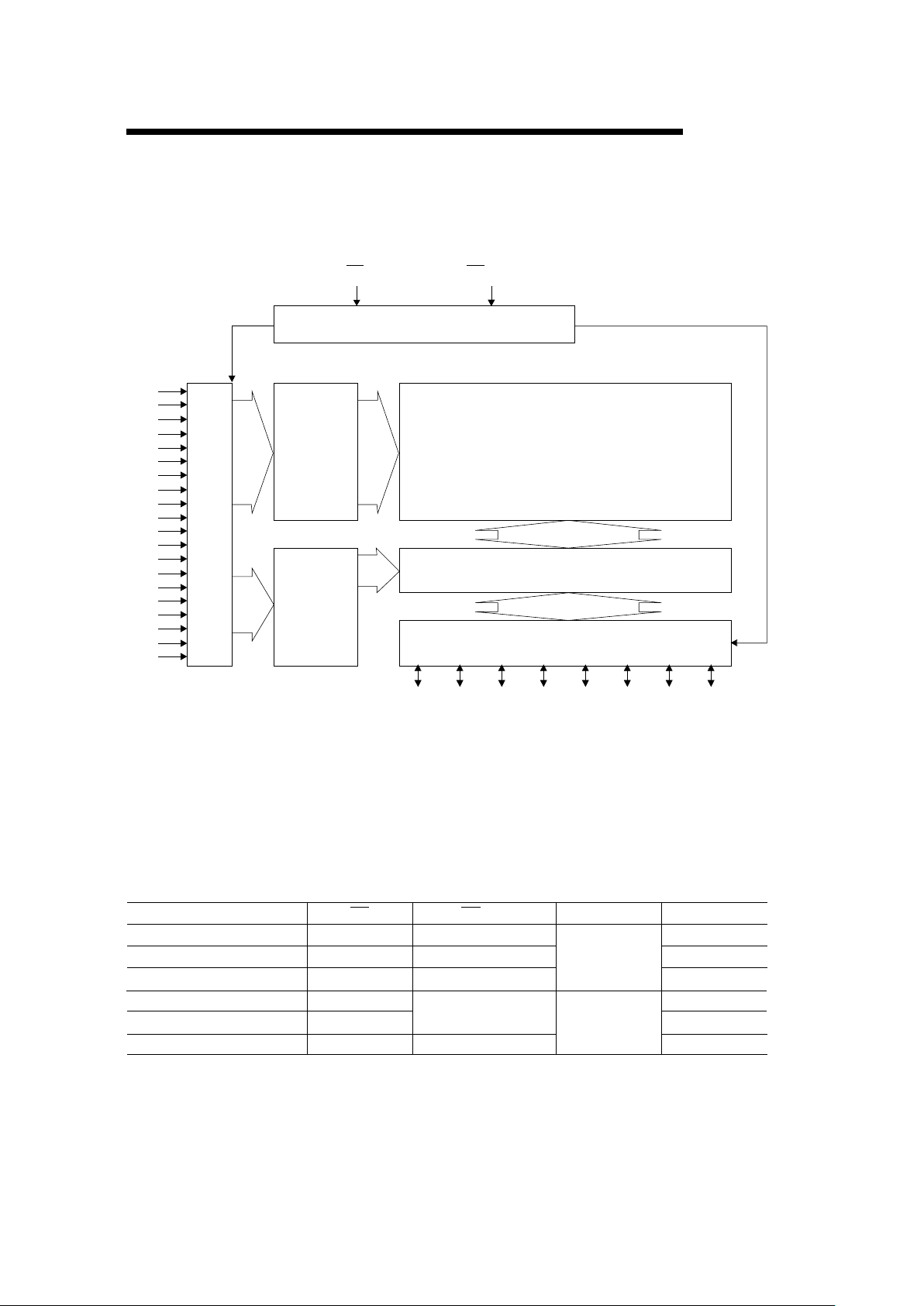
BLOCK DIAGRAM
FUNCTION TABLE
STAND-BY
READ
MODE
CE
V
CC
L
L
L
H
*: Don't Care
3.0V to 3.3V
D0 - D7
D
OUT
Hi-Z
Hi-Z
PROGRAM
D
IN
PROGRAM INHIBIT
Hi-Z
PROGRAM VERIFY
D
OUT
MR27V801D
OE/V
PP
A0
A1
A2
A3
A4
A5
A6
A7
A8
A9
A10
A11
A12
A13
A14
A15
A16
A17
A18
A19
D0
CE OE/V
PP
CE PGMOE
Address Buffer
Row Decoder
Column Decoder
Memory Matrix
Multiplexer
Output Buffer
D1 D2 D3 D4 D5 D6 D7
1,048,576X8-Bit
OUTPUT DISABLE
4.0V
H
L
L
H
L
*
9.75V
 Loading...