

OKI MR27V401DTA, MR27V401DMA, MR27V401DRA Datasheet

1/11
¡
The MR27V401D is a 4Mbit electrically Programmable Read-Only Memory organized as 524,288
word x 8bit. The MR27V401D operates on a single +3V-3.3V power supply and is TTL compatible.
Since the MR27V401D operates asynchronously , external clocks are not required , making this
device easy-to-use. The MR27V401D is suitable as large-capacity fixed memory for microcomputers
and data terminals. It is manufactured using a CMOS double silicon gate technology and is offered
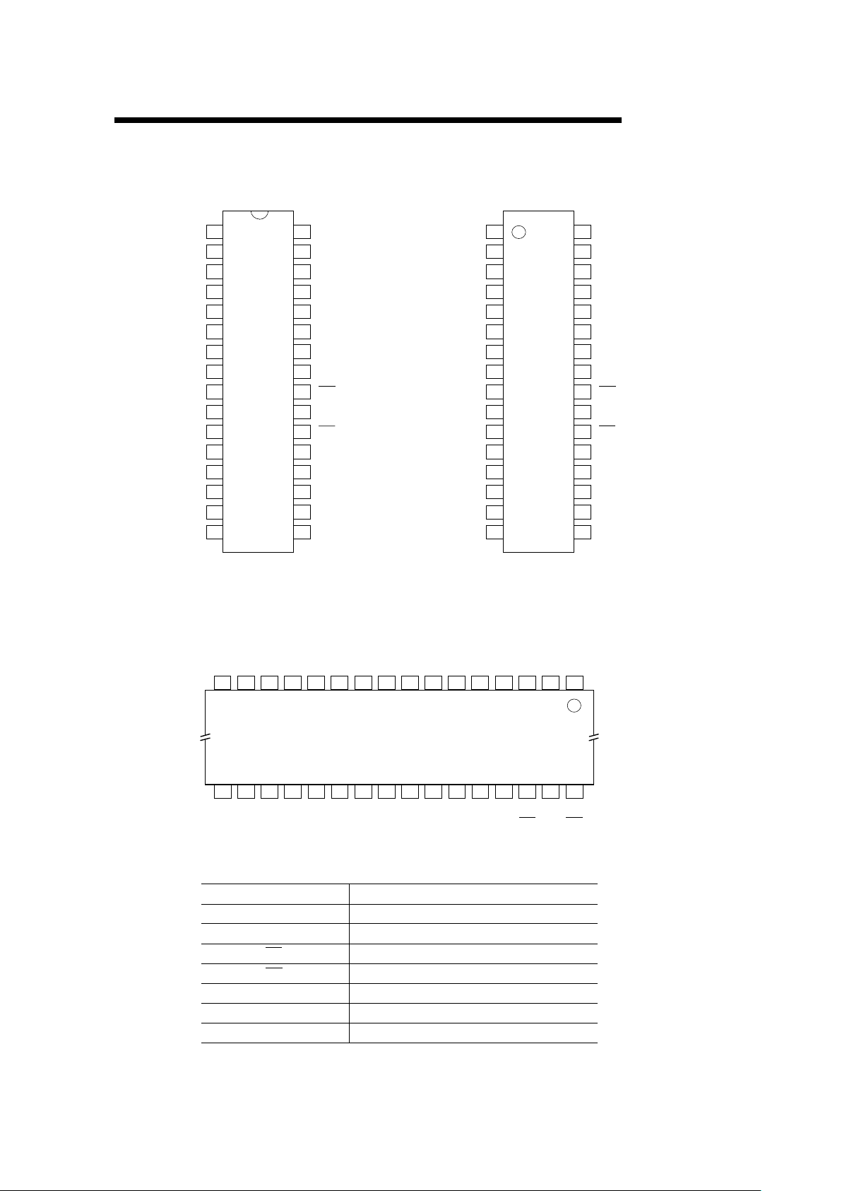
in 32-pin DIP, 32-pin SOP or 32-pin TSOP packages.
1A
MR27V401D
524,288-Word x 8-Bit One Time PROM
DESCRIPTION
FEATURES
• 524,288 word x 8bit
• Single +3V-3.3V power supply
• Access time 80ns access time (Vcc=+3V)
70ns access time (Vcc=+3.3V)
• Input / Output TTL compatible
• Three-state output
• Packages
32-pin plastic DIP (DIP32-P-600-2.54) (Product name : MR27V401DRA)
32-pin plastic SOP (SOP32-P-525-1.27-K) (Product name : MR27V401DMA)
32-pin plastic TSOP (TSOP I 32-P-814-0.50-K) (Product name : MR27V401DTA)
Semiconductor
November 1999
A10
2/11
PIN CONFIGURATION (TOP VIEW)
MR27V401D
PIN NAMES
FUNCTIONS
A0 - A18 Address input
D0 - D7 Data output
CE
Output enable
V
CC
Power supply voltage
OE
Chip enable
V
SS
GND
Vpp
A18
A17
A13
A8
A9
A11
D6
D5
D4
D3
A14
32
31
30
2
3
4
5
29
28
27
26
6
7
8
9
25
24
23
22
10
11
12
13
21
20
19
18
14
15
16 17
A16
A7
A6
A5
A4
A3
A2
D1
D2
1
CE
A15
A12
A1
A0
D0
V
SS
V
CC
OE
A10
D7
32-pin DIP
Vpp
A18
A17
A13
A8
A9
A11
D6
D5
D4
D3
A14
32
31
30
2
3
4
5
29
28
27
26
6
7
8
9
25
24
23
22
10
11
12
13
21
20
19
18
14
15
16 17
A16
A7
A6
A5
A4
A3
A2
D1
D2
1
CE
A15
A12
A1
A0
D0
V
SS
V
CC
OE
A10
D7
32-pin SOP
Vpp A18
A17
A13A8A9
A11A14
A16
A7
A6
A5
A4
A3
A2 D1
D2
CE
A15
A12
A1
A0
D0
V
SS
V
CC
OE
32-pin TSOP
32313029282726252423222120191817
12345678910111213141516
D3 D5 D7
D4 D6
V
PP
Program Power supply voltage
3/11
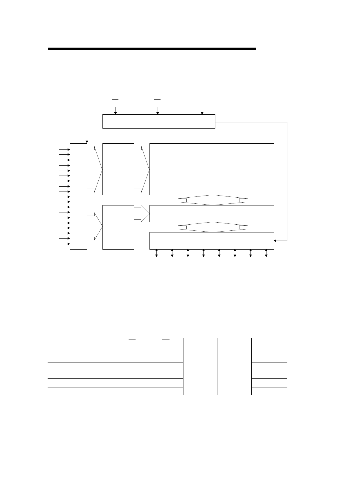
BLOCK DIAGRAM
FUNCTION TABLE
STAND-BY
READ
MODE
CE
V
CC
L
L
L
H
* : Don't Care (H or L)
3.0V to 3.3V
D0 - D7
D
OUT
Hi-Z
Hi-Z
PROGRAM
D
IN
PROGRAM INHIBIT
Hi-Z
PROGRAM VERIFY
D
OUT
MR27V401D
OE
A0
A1
A2
A3
A4
A5
A6
A7
A8
A9
A10
A11
A12
A13
A14
A15
A16
A17
A18
D0
CE OE
CE PGMOE
Address Buffer
Row Decoder
Column Decoder
Memory Matrix
Multiplexer
Output Buffer
D1 D2 D3 D4 D5 D6 D7
524,288X8-Bit
OUTPUT DISABLE
4.0V
H
H
L
H
L
*
9.75V
V
PP
V
PP
**
H
H
** : Don't Care (H or L or Open)
4/11
Operating temperature under bias
Storage temperature
Input voltage
Output voltage
Power supply voltage
Program power supply voltage
Power dissipation per package
Parameter
Symbol
Topr
UnitValueCondition
RECOMMENDED OPERATING CONDITIONS
VCC power supply voltage
VPP power supply voltage
Input "H" level
Input "L" level
Parameter Symbol
V
CC
Unit
3.6
Typ.
2.7
Condition
T
stg
V
I
V
O
V
CC
V
PP
P
D
0 to 70
-55 to 125
V-0.5 to V
CC
+ 0.5
V-0.5 to VCC + 0.5
V-0.5 to 5
V-0.5 to 11.5
W1.0
-
relative to V
SS
(Ta=0 to 70°C)
Min. Max.
V
VCC+0.5
-0.5
-
V
V
CC
+0.5*2.2
-
V
0.6-0.5**
-
V
V
PP
V
IH
V
IL
VCC=2.7V - 3.6V
Voltage is relative to Vss
ABSOLUTE MAXIMUM RATINGS
-
-
MR27V401D
°C
°C
* : Vcc+1.5V (Max.) when pulse width of overshoot is less than 10nS.
** : -1.5V (Min.) when pulse width of undershoot is less than 10nS.
 Loading...