


E2C0043-19-74
Preliminary
¡ Semiconductor ML9261/62
This version: Jul. 1999
¡ Semiconductor
ML9261/62
60-Bit Vacuum Fluorescent Display Tube Grid/Anode Driver
GENERAL DESCRIPTION
The ML9261/62 is a monolithic IC designed for directly driving the grid and anode of the vacuum
fluorescent display (VFD) tube. The device contains a 60-bit shift register, a 60-bit register circuit,
and 60 VFD tube driving circuits on a single chip.
Display data is serially stored in the shift register at the rising edge of a clock pulse.
Setting the CL pin low allows all the VFD tube driving circuits to be driven low, which makes it
possible to set the display blanking.
Also, setting both of the CL and CHG pins high allows all the VFD tube driving circuits to be
driven high, which provides the easy testing of all lights after final assembly of a VFD tube panel.
FEATURES
• Logic Supply Voltage (V
• Driver Supply Voltage (VHV): +60V
• Driver Output Current
• Directly connected to VFD tube by using push-pull output (Pull-down resistors are not
needed)
• Data Transfer Speed: 4MHz
• Package :
70-pin plastic SSOP (SSOP70-P-500-0.80-K) (Product names : ML9261MB and ML9262MB)
) : +3.3V±10% or +5.0V±10%
CC
I
OHVH1
I
OHVH2
I
OHVL
(Only one driver output : "H") : –40mA (V
(All the driver outputs : "H") : –120mA (V
:1mA
DISP
DISP
=40V)
=40V)
1/16
¡ Semiconductor ML9261/62
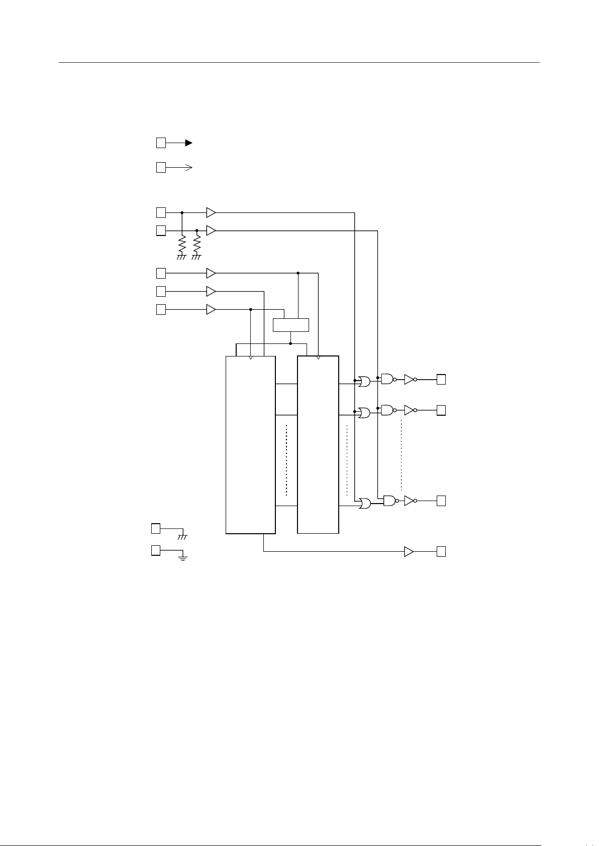
BLOCK DIAGRAM
V
DISP
V
DD
CL
CHG
LS
DIN
CLK
RESET
L-GND
D-GND
CSI
RRC
PO-1
PO-2
60-Bit
Shift
Register
P0-60
SO
D-1
O-1
D-2
O-2
60-Bit
Register
D-60 O-60
HVO 1
HVO 2HVO
HVO60
DOUT
2/16

¡ Semiconductor ML9261/62
INPUT AND OUTPUT CONFIGURATION
3/16

¡ Semiconductor ML9261/62
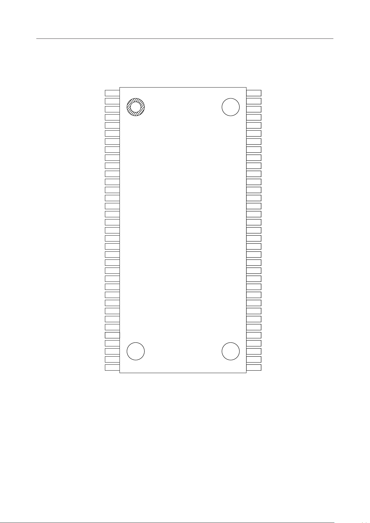
PIN CONFIGURATION (TOP VIEW)
ML9261
HVO 25
HVO 24
HVO 23
HVO 22
HVO 21
HVO 20
HVO 19
HVO 18
HVO 17
HVO 16
HVO 15
HVO 14
HVO 13
HVO 12
HVO 11
HVO 10
HVO 9
HVO 8
HVO 7
HVO 6
HVO 5
HVO 4
HVO 3
HVO 2
HVO 1
V
DISP
V
D
D
OUT
CLK
CHG
L-GND
D-GND
1
2
3
4
5
6
7
8
9
10
11
12
13
14
15
16
17
18
19
20
21
22
23
24
25
26
27
DD
28
IN
29
30
31 40
LS HVO 56
32
CL
33
34
35
70
69
68
67
66
65
64
63
62
61
60
59
58
57
56
55
54
53
52
51
50
49
48
47
46
45
44
43
42
41
39
38
37
36
HVO 26
HVO 27
HVO 28
HVO 29
HVO 30
HVO 31
HVO 32
HVO 33
HVO 34
HVO 35
HVO 36
HVO 37
HVO 38
HVO 39
HVO 40
HVO 41
HVO 42
HVO 43
HVO 44
HVO 45
HVO 46
HVO 47
HVO 48
HVO 49
HVO 50
HVO 51
HVO 52
HVO 53
HVO 54
HVO 55
HVO 57
HVO 58
HVO 59
HVO 60
70-Pin Plastic SSOP
(SSOP70-P-500-0.80-K)
4/16
¡ Semiconductor ML9261/62
PIN CONFIGURATION (TOP VIEW)
ML9262
D-GND
L-GND
CHG
CLK
D
OUT
D
V
V
DISP
HVO 1
HVO 2
HVO 3
HVO 4
HVO 5
HVO 6
HVO 7
HVO 8
HVO 9
HVO 10
HVO 11
HVO 12
HVO 13
HVO 14
HVO 15
HVO 16
HVO 17
HVO 18
HVO 19
HVO 20
HVO 21 HVO 30
HVO 22
HVO 23
HVO 24
HVO 25
1
2
3
4
CL
5
LS
6
7
8
IN
9
DD
10
11
12
13
14
15
16
17
18
19
20
21
22
23
24
25
26
27
28
29
30
31 40
32
33
34
35
70
69
68
67
66
65
64
63
62
61
60
59
58
57
56
55
54
53
52
51
50
49
48
47
46
45
44
43
42
41
39
38
37
36
HVO 60
HVO 59
HVO 58
HVO 57
HVO 56
HVO 55
HVO 54
HVO 53
HVO 52
HVO 51
HVO 50
HVO 49
HVO 48
HVO 47
HVO 46
HVO 45
HVO 44
HVO 43
HVO 42
HVO 41
HVO 40
HVO 39
HVO 38
HVO 37
HVO 36
HVO 35
HVO 34
HVO 33
HVO 32
HVO 31
HVO 29
HVO 28
HVO 27
HVO 26
70-Pin Plastic SSOP
(SSOP70-P-500-0.80-K)
5/16
¡ Semiconductor ML9261/62
PIN DESCRIPTION
Symbol Description
CLK
DIN
DOUT
LS
CL
Type
I
I
O
I
I
Shift register clock input pin.
Shift register reads data from DIN while the CLK pin is low and the data in the shift register
is shifted from one stage to the next stage at the rising edge of the clock.
Serial data input pin of the shift register.
Display data (positive logic) is input in the DIN pin in synchronization with clock.
Serial data output pin of the shift register.
Data is output from the DOUT pin in synchronization with the CLK signal.
Latch strobe input pin.
The contents of the parallel outputs (PO1 to PO60) of the shift register are read at the rising
edge of LS (edge-triggered). When the CLK rises while LS is high, the parallel outputs
(PO1 to PO60) and latch outputs (O1 to O60) go low.
Clear input pin with a built-in pull-down resistor.
The CL pin is normally set high.
If the CL pin is high and the CHG pin is low, the driver outputs (HV01 to HV60) are in phase
with the corresponding register outputs (O1 to O60).
If the CL pin is high and the CHG pin is high, the driver outputs (HV01 to HV60) are high
irrespective of the states of the register outputs.
If the CL pin is set low, the driver outputs are driven low irrespective of the states of the
CHG pin and register outputs.
This allows display blanking to be set.
CHG
VHO1-60
V
DISP
V
DD
D-GND
L-GND
Input for testing (with a pull-down resistor).
The CL pin is normally set low.
If the CHG pin is low and the CL pin is high, the driver outputs (HV01 to HV60) are in phase
with the corresponding register outputs (O1 to O60).
I
If the CHG pin is low and the CL pin is low, the driver outputs (HV01 to HV60) are low
irrespective of the states of the register outputs.
If the CHG pin is set high, the driver outputs are driven high irrespective of the states of the
register outputs.
This provides the easy testing of all lights after final assembly.
High voltage driver outputs for driving VFD tube.
O
If the CL pin is high and the CHG pin is low, the driver outputs are in phase with the
corresponding register outputs (O1 to O60).
The direct connection to the grid or anode of a VFD tube eliminates pull-down resistors.
Power supply pin for driver circuits of VFD tube
Power supply pin for logic
GND pin for driver circuits of a VFD tube.
Since the D-GND is not be connected to L-GND, connect this pin to the external L-GND.
GND pin for the logic circuits.
Since the L-GND pin is not be connected to D-GND, connect this pin to the external D-GND.
6/16

¡ Semiconductor ML9261/62
ABSOLUTE MAXIMUM RATINGS
Parameter Symbol Condition Rating Unit
Supply Voltage (1) V
Supply Voltage (2) V
Input Voltage V
Output Voltage V
*1
*1, *2
*1
*1
Output Current I
Withstand Output Voltage
*1, *2
V
Power Dissipation P
Package Thermal Resistance
*3
Storage Temperature T
DD
DISP
IN
O
HVO
R
j-a
STG
O
D
Applicable to logic supply pin
Applicable to driver supply pin
Applicable to all input pins
Applicable to DOUT
Notes: *1 Supply Voltage with respect to L-GND and D-GND
*2 Permanent damage may be caused if the voltage is supplied over the rating value.
*3 Package Thermal Resistance (between junction and ambient)
The junction temperature (Tj) expressed by the equation indicated below should not
exceed 150°C.
Tj=P ¥ R
+Ta (P: Maximum power consumption)
j–a
–0.3 to +6.5 V
–0.3 to +65 V
–0.3 to VDD +0.3 V
–0.3 to VDD +0.3 V
–50 to 0.0 mAApplicable to HVO1 to 60
–0.3 to V
DISP
+0.3 VApplicable to HVO1 to 60
860
145 °C/WTa > 25°C
–55 to +150 °C—
mWTa £ 25°C
7/16

¡ Semiconductor ML9261/62
RECOMMENDED OPERATING CONDITIONS-1
Unit Power Supply: 5.0V (Typ.)
Parameter Max
Power Supply (1)
Power Supply (2)
"H" Input Voltage
"L" Input Voltage
Driver Output Current
CLK Frequency
Operating Temperature °C
Symbol Condition
V
DD
V
DISP
V
IH
V
IL
I
OHVH1
I
OHVH2
f
CLK
T
OP
Applicable to all inputs
Applicable to all inputs
Only 1 output is ON.
All outputs are ON.
—
—
—
—
Min
4.5
20
0.7V
—
—
—
—
–40
Typ. Unit
5.0
—
DD
—
—
—
—
—
—
5.5
60
—
0.3V
–40
–120
4.0
+85
DD
RECOMMENDED OPERATING CONDITIONS-2
Unit Power Supply: 3.3V (Typ.)
Parameter Max
Power Supply (1)
Power Supply (2)
"H" Input Voltage
"L" Input Voltage
Driver Output Current
CLK Frequency
Operating Temperature °C
Symbol Condition
V
DD
V
DISP
V
IH
V
IL
I
OHVH1
I
OHVH2
f
CLK
T
OP
Applicable to all inputs
Applicable to all inputs
Only 1 output is ON.
All outputs are ON.
—
—
—
—
Min
3.0
20
0.8V
—
—
—
—
–40
Typ. Unit
3.3
—
DD
—
—
—
—
—
—
3.6
60
—
0.2V
–40
–120
4.0
+85
DD
V
V
V
V
mA
mA
MHz
V
V
V
V
mA
mA
MHz
8/16

¡ Semiconductor ML9261/62
ELECTRICAL CHARACTERISTICS
DC Characteristics-1
(V
=4.5 to 5.5V, V
DD
Parameter Max
Symbol
"H" Input Voltege
"L" Input Voltage
"H" Input Current
"L" Input Current
Input Capacitance
"H" Output Voltage IOH=–0.1mA
"L" Output Voltage IOL=0.1mA
Supply Current
(Design Goal)
I
I
Applicable pin Condition
V
IH
V
IL
I
IH1
I
IH2
I
IL
C
IN
V
OH1
V
OH2
V
OL1
V
OL2
I
DD1
I
DD2
DISP1
DISP2
All inputs
All inputs
DIN, CLK, LS
CL, CHG
All inputs
All inputs
DOUT
HVO1 to 60
DOUT
HVO1 to 60
V
DD
V
DD
V
DISP
V
DISP
No load
—
—
V
DD=VIN
=5.5V
VDD=VIN=5.5V
V
=5.5V,VIN=0V
DD
Ta=25°C
IOH=–40mA
IOL=1mA
All inputs: "L"
All inputs: "H"
All inputs: "L"
All inputs: "H"
Min
0.7V
—
–1.0
–1.0
—
DISP
—
—
—
—
=40V, Ta=–40 to +85°C)
DISP
Typ. Unit
DD
—
—
—
0.3V
+1.0
—805.0
—
+1.0
15
——VDD–1
–4
——V
— 1.1—
— 3.0—
—
—
—
—
10.0
10.0
10.0
10.0
—
—
DD
V
V
mA
mA
mA
pF
V
V
V
V
mA
mA
mA
mA
DC Characteristics-2
(V
=3.0 to 3.6V, V
DD
Parameter Max
Symbol
"H" Input Voltege
"L" Input Voltage
"H" Input Current
"L" Input Current
Input Capacitance
"H" Output Voltage IOH=–0.1mA
"L" Output Voltage IOL=0.1mA
Supply Current
(Design Goal)
I
I
Applicable pin Condition
V
IH
V
IL
I
IH1
I
IH2
I
IL
C
IN
V
OH1
V
OH2
V
OL1
V
OL2
I
DD1
I
DD2
DISP1
DISP2
All inputs
All inputs
DIN, CLK, LS
CL, CHG
All inputs
All inputs
DOUT
HVO1 to 60
DOUT
HVO1 to 60
V
DD
V
DD
V
DISP
V
DISP
No load
—
—
V
DD=VIN
=3.3V
VDD=VIN=3.3V
V
=3.3V,VIN=0V
DD
Ta=25°C
IOH=–40mA
IOL=1mA
All inputs: "L"
All inputs: "H"
All inputs: "L"
All inputs: "H"
Min
0.8V
—
–1.0
–1.0
—
DISP
—
—
—
—
=40V, Ta=–40 to +85°C)
DISP
DD
–4
Typ. Unit
—
—
—
—502.0
—
15
——VDD–1
——V
— 1.1—
— 3.0—
—
—
—
—
—
0.2V
+1.0
+1.0
—
10.0
10.0
10.0
10.0
DD
V
V
mA
mA
mA
pF
V
V
V
V
mA
mA
mA
mA
9/16

¡ Semiconductor ML9261/62
AC Characteristics-1
(VDD=4.5 to 5.5V, V
Parameter
CLK Pulse Width
DIN Setup Time ns
DIN Hold Time
CLK-LS Setup Time
LS-CLK Setup Time
tW (CLK)
t
(D-CLK)
SU
tH (CLK-D)
t
(CLK-LS)
SU
t
(LS-CLK)
SU
Condition
During normal operation
At display data reset
CLK-LS Hold Time
LS-CHG Setup Time
LS-CL Setup Time
LS Pulse Width
CHG Pulse Width
CL Pulse Width
DOUT Delay time
Driver Output Delay Time
Driver Output Slew Rate
(CLK-L)
t
H
t
(LS-CHG)
SU
t
(LS-CL)
SU
t
W
tW (CHG)
t
W
t
PD
t
t
t
DRHL
t
t
(LS)
(CL)
, t
PRD
DLH
DHL
TLH
THL
At display data reset
Load: 30pF
Load: 2.0kW resistance in
parallel with 20pF capacitance
Load: 2.0kW resistance in
parallel with 20pF capacitance
=40V, Ta=–40 to +85°C)
DISP
Max.Min. UnitSymbol
80 ns
150
50 —
50 ns
50
50
50
80
10
—
—
—
—
—
—
—
—
5.0
5.0
ns
ns
ns50 —tSU (L-CLK)
ns50 —
ns
ns50 —
ns
ms
ms10 —
ns—50
ms— 1.0
ms— 1.0
ms— 1.0
ms
ms
AC Characteristics-2
Parameter
CLK Pulse Width
DIN Setup Time
DIN Hold Time
CLK-LS Setup Time
LS-CLK Setup Time
CLK-LS
LS-CHG Setup Time
LS-CL Setup Time
LS Pulse Width
CHG Pulse Width
CL Pulse Width
DOUT Delay time
Driver Output Delay Time
Driver Output Slew Rate
tH (CLK-D)
t
(CLK-LS)
SU
t
(LS-CLK)
SU
t
(CLK-L)
H
t
(LS-CHG)
SU
t
(LS-CL)
SU
t
(LS)
W
tW (CHG)
t
(CL)
W
t
, t
PD
PRD
t
DLH
t
DHL
t
DRHL
t
TLH
t
THL
(VDD=3.0 to 3.6V, V
Condition
During normal operation
At display data reset
At display data reset
Load: 30pF
Load: 2.0kW resistance in
parallel with 20pF capacitance
Load: 2.0kW resistance in
parallel with 20pF capacitance
=40V, Ta=–40 to +85°C)
DISP
Max.Min. UnitSymbol
15080 nstW (CLK)
—50 nstSU (D-CLK)
50 ns
50
50
50
80
10
—
—
—
—
—
—
—
—
5.0
5.0
ns
ns
ns50 —tSU (L-CLK)
ns50 —
ns
ns50 —
ns
ms
ms10 —
ns—50
ms— 3.0
ms— 3.0
ms— 3.0
ms
ms
10/16

¡ Semiconductor ML9261/62
11/16
TIMING DIAGRAM
Normal Display Operation
CLK
DIN
LS
HVO (OTHERS)
CL
HVO (1, 2, 59, 60)
CHG
DOUT
T1/2 T3/4
T59/60 T1/2 T3/4
t
SU
(D-CLK)
t
PD
t
SU
(CLK-LS)
t
SU
(LS-CLK)
t
SU
(LS-CHG)
t
W
(CHG)
t
SU
(LS-CL)
t
W
(CL)
t
W
(CL)
t
DLH
t
DLH
t
DHL
t
DHL
t
TLH
t
TLH
t
THLtTHL
t
H
(CLK-D)
t
W
(CHG)
1/f
CLK
t
W
(CLK)
t
PD
t
W
(LS)

¡ Semiconductor ML9261/62
12/16
Display Data Reset Operation
CLK
DIN
LS
HVO (OTHERS)
CL
HVO (1, 2, 59, 60)
CHG
DOUT
T1/2 T3/4
T59/60 T1/2
t
PRD
t
DRHL
t
SU
(L-CLK)
t
H
(CLK-L)

¡ Semiconductor ML9261/62
FUNCTIONAL DESCRIPTION
Display Data Reset
When the power is turned on, the shift register outputs (PO1 to PO60) and register outputs (O1
to O60) are indeterminate. Consequently the display of a VFD tube may flickers because
unnecessary driver outputs go high. To prevent such flicker, it is required to perform the
following operations.
1. Turn on the logic power supply while the CL input is kept low.
2. Set the LS input high.
3. Switch the CLK input from a low level to a high level at least once.
By performing the above operations, the shift register outputs (PO1 to PO60) and register outputs
(O1 to O60) all are set low.
4. Enter display data.
5. Set the CL input high.
Data Transfer
Write display data by using a serial transfer.
Serial data is input in the shift register at the rising edge of a CLK input pulse.
When the LS input rises, display data is written in the latch.
Driver Output Control
1. To turn on or off driver outputs by using display data transfered into the shift register, set the
CL input high and set the CHG input low.
2. To set all the driver outputs low, set the CL input low.
3. To set all the driver outputs high, set the CL input and CHG input high at a time.
13/16

¡ Semiconductor ML9261/62
j
Function Table
Shift register
Register
Input
CLK
H H PO1n
L
X
XLLH
X: Don't Care
PO1n to PO59n: PO1 to PO59 data
X: Don't Care, m: 1 to 60
LS
L
L
L
Input
CLK
X
X
X
PO1DIN
L
PO1n
LS
H
PO2
PO2n
PO2n
ust before CLOCK rises.
Shift Register Parallel Out Latch Output
POm Om
HH
LL
X No Change
LL
PO59
PO58n
PO58n
PO59n
L
PO60
PO59n
PO59n
PO60n
L
OutputShift Register Parallel Out
DOUT
PO59n
PO59n
PO60n
L
Driver output
Input
CL
X: Don't Care, m: 1 to 60
CHG
H
H
H
L
XX H
L
L
H
X
CLK
X
X
X
X
LS
Latch Output Output
Om HVOm
X
X
X
X
HH
LL
XH
XL
LL
14/16

¡ Semiconductor ML9261/62
Test circuit
20pF
V
DISP
V
DD
DIN CLK LS CL CHG
HVO1
1.0kW
20pF
HVO1
1.0kW
20pF
HVO1
1.0kW
30pF
DOUT
D-GNDL-GND
15/16
¡ Semiconductor ML9261/62
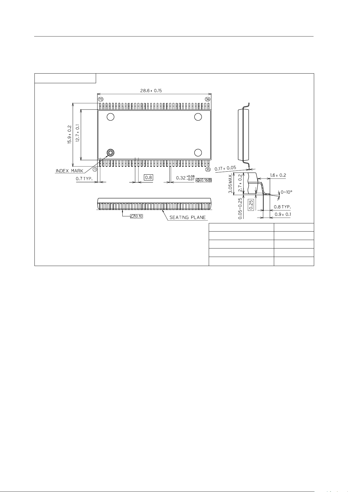
PACKAGE DIMENSIONS
(Unit : mm)
SSOP70-P-500-0.80-K
Mirror finish
Package material
Lead frame material
Pin treatment
Solder plate thickness
Package weight (g)
Epoxy resin
42 alloy
Solder plating
5 mm or more
2.15 TYP.
Notes for Mounting the Surface Mount Type Package
The SOP, QFP, TSOP, SOJ, QFJ (PLCC), SHP and BGA are surface mount type packages, which
are very susceptible to heat in reflow mounting and humidity absorbed in storage.
Therefore, before you perform reflow mounting, contact Oki’s responsible sales person for the
product name, package name, pin number, package code and desired mounting conditions
(reflow method, temperature and times).
16/16

E2Y0002-29-62
NOTICE
1. The information contained herein can change without notice owing to product and/or
technical improvements. Before using the product, please make sure that the information
being referred to is up-to-date.
2. The outline of action and examples for application circuits described herein have been
chosen as an explanation for the standard action and performance of the product. When
planning to use the product, please ensure that the external conditions are reflected in the
actual circuit, assembly, and program designs.
3. When designing your product, please use our product below the specified maximum
ratings and within the specified operating ranges including, but not limited to, operating
voltage, power dissipation, and operating temperature.
4. Oki assumes no responsibility or liability whatsoever for any failure or unusual or
unexpected operation resulting from misuse, neglect, improper installation, repair, alteration
or accident, improper handling, or unusual physical or electrical stress including, but not
limited to, exposure to parameters beyond the specified maximum ratings or operation
outside the specified operating range.
5. Neither indemnity against nor license of a third party’s industrial and intellectual property
right, etc. is granted by us in connection with the use of the product and/or the information
and drawings contained herein. No responsibility is assumed by us for any infringement
of a third party’s right which may result from the use thereof.
6. The products listed in this document are intended for use in general electronics equipment
for commercial applications (e.g., office automation, communication equipment,
measurement equipment, consumer electronics, etc.). These products are not authorized
for use in any system or application that requires special or enhanced quality and reliability
characteristics nor in any system or application where the failure of such system or
application may result in the loss or damage of property, or death or injury to humans.
Such applications include, but are not limited to, traffic and automotive equipment, safety
devices, aerospace equipment, nuclear power control, medical equipment, and life-support
systems.
7. Certain products in this document may need government approval before they can be
exported to particular countries. The purchaser assumes the responsibility of determining
the legality of export of these products and will take appropriate and necessary steps at their
own expense for these.
8. No part of the contents contained herein may be reprinted or reproduced without our prior
permission.
9. MS-DOS is a registered trademark of Microsoft Corporation.
Copyright 1999 Oki Electric Industry Co., Ltd.
Printed in Japan
 Loading...